
Normally-off AlGaN/GaN heterojunction field-effect transistors with in-situ AlN gate insulator
2022-12-28 09:55:12TaofeiPu蒲濤飛ShuqiangLiu劉樹強(qiáng)XiaoboLi李小波TingTingWang王婷婷JiyaoDu都繼瑤LiuanLi李柳暗LiangHe何亮XinkeLiu劉新科andJinPingAo敖金平
Chinese Physics B 2022年12期
Taofei Pu(蒲濤飛) Shuqiang Liu(劉樹強(qiáng)) Xiaobo Li(李小波) Ting-Ting Wang(王婷婷) Jiyao Du(都繼瑤)Liuan Li(李柳暗) Liang He(何亮) Xinke Liu(劉新科) and Jin-Ping Ao(敖金平)
1Hanshan Normal University,Chaozhou 521041,China
2No. 5 Electronics Research Institute of the Ministry of Industry and Information Technology,Guangzhou 510610,China
3Shenzhen University,Shenzhen 518000,China
4School of Microelectronics,Xidian University,Xi’an 710071,China
5School of Automation and Electrical Engineering,Shenyang Ligong University,Shenyang 110159,China
6Yibin Research Institute,Jilin University,Yibin 644000,China
Keywords: AlGaN/GaN HFET,normally-off,in-situ AlN,metal–insulator–semiconductor
1. Introduction
Normally-off AlGaN/GaN heterostructure field-effect transistors (HFETs) have attracted much attention for power switching applications because of their inherent fail-safe property, simple circuit configuration and high electron mobility of two-dimensional electron gas (2DEG).[1–3]Generally,a threshold voltage (Vth) higher than 3.0 V as well as a gate voltage swing of 10 V are desirable to avoid the malfunction caused by noise.[4]For some special power switching applications, aVthof 6.0 V is desired to prevent the power switches from faulty turn-on induced by the electromagnetic interference.[5]In terms of realizing normally-off operation,the p-GaN cap layer structure demonstrates tremendous advantages such as high channel mobility, goodVthuniformity and suitable for integration.[6–11]Based on those advantages,the AlGaN/GaN HFETs with p-GaN cap layer become the unique commercial solution to achieve the normally-off operation with respect to gate recess,fluorine ion treatment,ultrathin barrier, and so on.[12,13]On the basis of simulation and experiment results, theVthof p-GaN HFET presents a relationship with the contact type between the gate electrode and p-GaN. Usually, the ohmic type gate can be formed by depositing and/or oxidizing Ni,NiOx,or Pt on p-GaN layer.[7,8]However,due to the low hole concentration in p-GaN,theVthis usually limited to around 1 V. Furthermore, the p-GaN/n-GaN junction turns on at a relatively small forward bias,leading to the huge gate leakage current.[14,15]Then,the Schottky type gate formed by a low work function metal on p-GaN is proposed to raise theVthto approximately 2 V and suppress the gate leakage current. The mechanism is attributed to that the reverse biased Schottky junction undertakes partial of the gate bias.[16,17]However,the Schottky junction also hindrances the transport of the hole, resulting in theVthinstability when the gate voltage sweeps to a high positive values.In addition,even with the Schottky type gate,theVthstill does not meet the requirement of 3 V or even higher for practical applications.
To obtain a higher positiveVth,we previously proposed a metal–insulator–semiconductor(MIS)gate structure,in which a thin dielectric layer(especially high-kdielectric)was introduced below the gate metal electrode.[6]For the conventional device fabrication process, the gate electrode is deposited after the growth of dielectric layer and not covers all the gate area due to the alignment limitation.[18]This non-self-aligned gate structure can eliminate the leakage path along the sidewall of p-GaN, showing an off-state blocking capability after forward gate breakdown.[19]However,the gate electrode needs to cover the gate region totally to reduce the channel resistance.We have developed a gate-first process with the low temperature ohmic annealing and realized the self-aligned gate stacks to optimize the device performance. It is well known that the device performance of MIS structure directly relates with the insulator properties, such as band offset, the dielectric constant,and polarization. However,the effect of dielectric material on the device characteristics is rarely reported.
In this article, we fabricated normally-off p-GaN/AlGaN/GaN HFETs within-situAlN gate dielectric layer by using the simple conventional gate-last process.Compared to theVthof 1.2 V and gate swing of 6 V for the p-GaN HFETs with 5 nm SiNxdielectric layer,the device with 5 nm AlN layer presents a highVthof 4 V, a high gate swing of 13 V,as well as a high gate breakdown voltage. Furthermore,a similar maximum channel electron field-effect mobility of around 1500 cm2·V?1·s?1is extracted for both devices.
2. Device structure and fabrication
The schematic view of device structures with AlN layer(labeled as AlN gate) and SiNxlayer (labeled as SiNxgate)are shown in Figs. 1(a) and 1(b), respectively. The Al-GaN/GaN heteroepitaxial structure was grown on a Si substrate by metal organic chemical vapor deposition(MOCVD).The structure of the wafer along the vertical direction consists of a buffer layer, a carbon-doped high-resistance GaN and an Al0.24Ga0.76N/GaN (10/300 nm) heterostructure from bottom to top. Then, 3 nm i-GaN and 100 nm p-GaN cap layer were grown to realize the normally-off operation. Hole concentration in the p-GaN layer was confirmed to be about 2×1017cm?3after high temperature activation in N2ambient, and the activation ratio was around 1%–2%. To realize the AlN gate structure, 5 nm AlN layer wasin-situgrown in MOCVD on the top of the p-GaN layer.

Fig. 1. Schematic structures of the devices with AlN (a) and SiNx (b)gate insulator.
For the AlN gated device, the standard photolithography and lift-off technology was adopted. After cleaning by sulfuric peroxide mixture (SPM) and organic solution, the device isolation was conducted by inductively coupled plasma(ICP)dry etching with an etching depth of 120 nm. Then, p-GaN at non-gate region was removed by a low damage recipe with ICP/bias of 100/20 W and SiCl4etching gas.[8]Before the deposition of ohmic metal, a ICP plasma treatment was carried out on the ohmic region to realize the low temperature annealing process. The recipe was ICP/bias 100/100 W at 0.5 Pa for 12 s. Ti/Al/Ti/Au (20/200/40/40 nm) ohmic metal stacks were then deposited by magnetron sputtering and annealed at 500?C for 20 min in N2ambient. Finally, Ni/TiN(150/150 nm)gate stacks were deposited by magnetron sputtering. For the SiNxgated device,5 nm SiNxlayer was grown by plasma enhanced chemical vapor deposition (PECVD) at 350?C.Then,the sample was annealed at 900?C for 10 min in N2ambient to improve the SiNx/GaN interface quality. The following fabrication processes are the same as the AlN gated one.
3. Device performances
The output and transfer characteristics are recorded as shown in Fig. 2. A ring-type device (inset of Fig. 2(b))is adopted to avoid the leakage from isolation region. The gate length(Lg)and effective gate width(Wg)are 94μm and 819 μm, respectively. The outputI–Vcharacteristics of AlN and SiNxgated devices are measured with the gate voltage(Vg)sweeping from?2 V to 10 V and 6 V,respectively(Fig.2(a)).Good pinch-off characteristics are observed for both devices.The maximum current densities of the AlN and SiNxgated devices are around 13 mA/mm at aVgof 10 V. In addition, the scaled AlN gated device (Lg=3 μm) can achieve a current density of approximately 50 mA/mm at aVgof 10 V.The semilog transfer characteristics are shown in Fig. 2(b), in which the AlN gated device presents a sight higher on/off ratio(over 108)than that of the SiNxgated one. The sub-threshold swing(SS)for SiNxgated device extracted from Fig.2(b)is approximately 94.5 mV/dec (@Vd=10 V). Meanwhile, a largerSSfor AlN gate can be speculated from the semi-log plot of transfer characteristic,which is dominated by sub-threshold region as shown in Fig. 2(b). This relatively largerSSis possible to be caused by forward gate leakage current which originates from the thin barrier and gate dielectric layer. In sub-threshold region(labeled as I)of AlN gate in Fig.2(b),the transfer characteristic curve shows a gradually raising from 1 V to 3 V,demonstrating an obvious inflection point with respect to the following curve. Observed from Fig. 3(b), the gate leakage current is comparable with the drain current in region I, indicating that the drain current in sub-threshold region originates from the gate leakage current. A possible reason is ascribed to the difficulty in growth of AlN with high crystalline quality. WhenVgbeyond 3 V, the 2DEG channel is gradually conducting,and drain current is slowly increasing. Therefore, the transfer characteristic curve has an inflection point at 3 V for the AlN gated device. In addition, theVth(defined asId=0.01 mA/mm) are approximately 4 V and 1.2 V for the AlN and SiNxgated devices, respectively. The variation ofVthcan also be confirmed from the transfer characteristic of the linearId–Vgplot in Fig. 3(a). In addition, the maximum values of transconductance for SiN and AlN gated devices are approximately 7 mS/mm and 11 mS/mm, respectively. The relatively low transconductance is mainly ascribed to the large gate dimension and large distance between 2DEG channel and gate electrode.

Fig.2. (a)The output characteristics of the ring-type devices with AlN gate and SiNx gate. (b)The semi-log plot of the corresponding transfer characteristics.
The gate leakage current of both devices is closed to 10?9A level in reverse direction due to existing of gate dielectric and p–n junction. In forward direction,the gate leakage current of SiNxgated device reaches 1 mA at gate voltage of 6 V.However,the AlN gated demonstrates much lower forward gate leakage current even gate voltage over 10 V.In our experiment, the SiN is grown by PECVD with a low thickness of 5 nm. There may be many pinholes existed in the SiNx, resulting in the high leakage current. The band offset between AlN and AlGaN is enhanced obviously than that of SiNx/AlGaN interface. Meanwhile,the Fig.3(b)also demonstrates the hole injection phenomenon for AlN gated device.There are two fitting lines, intersecting atVgof 8.2 V, which indicates that the hole injection phenomenon occurs only until a relatively highVg.[20]Therefore,the AlN dielectric layer is similar with the barrier layer, which can suppress the hole injection efficiently.

Fig.3. (a)The linear transfer and transconductance characteristic,and(b)gate current–voltage characteristics for both kinds of gates.
The mechanisms ofVthdifference between two kinds of devices are discussed as following. We simulated the energy band diagrams (through Silvaco) of the AlN and SiNxgated devices without gate bias (Vgof 0 V) in Fig. 4(a). The normally off operation is confirmed because the condition band at the 2DEG channel is above the Fermi level for both devices.It was worthy noting that the conduction band offset and the energy band bending at the interface of AlN/p-GaN is more obvious than that of SiNx/p-GaN induced by the large bandgap and strong polarization effect of AlN layer, which may cause a much wider depletion region.[21]Thus, the depletion layer would extend and sustains more voltage under the positive gate bias. In addition, theVthis proportional to the thickness of gate dielectric in MIS gate structure,which is consistent with the experimental data in previous reports.[22]However, there is discrepancy in theVthand current density between the simulation and experimental values,which may be ascribed to the fix charge,interface defect,leakage current and so on. Firstly,according to our previous work,theVthof SiNxgate would be influenced by the deposition process of SiNxlayer. The hole at surface of the p-GaN(approximately 20 nm)is depleted by hydrogen due to the PECVD process.[6]This influence of hydrogen on hole concentration may be suppressed by thein-situgrown AlN layer. Secondly,it was reported that a high density of positive charge presents at the PECVD-SiNx/GaN interface,which may cause a negativeVthshifting. Therefore, the gate metal/AlN/p-GaN stack can undertake more forward bias than that of SiNxgated one,resulting in a higherVth.

Fig. 4. The simulated energy band diagrams at Vg of 0 V (a) and transfer characteristics (b) for SiNx and AlN gated devices with different dielectric thickness.

Fig.5. The field-effect mobility(a)and the gate breakdown voltage(b)for AlN and SiNx gated devices,respectively.
Additionally, the field-effect channel electron mobility(μFE)of the AlN and SiNxgated devices are calculated based on the capacitance–transconductance method and plotted in Fig. 5(a).[7]The maximum field-effect mobility for the AlN and SiNxgated devices are comparable to each other(around 1500 cm2·V?1·s?1). Those values are close to that of the 2DEG channel in the AlGaN/GaN HFETs,indicating that both the SiNxlayer (grown by PECVD) and thein-situAlN layer(grown by MOCVD) have no obvious effect on the channel mobility. Moreover, the gate breakdown voltage (VgBD) is provided in Fig. 5(b). The AlN gated device demonstrates a lower gate leakage current than that of SiNxgated one. Then,the gate swing of the AlN gated device can be enhanced to approximately 13 V (defined by reachingIgof 1 mA/mm). As plotted in Fig. 6, besides the increase ofVth, another advantage of the introduction of dielectric is the suppression of gate leakage and the enhanced gate breakdown voltage. Compared with several reported p-GaN gate HEMTs,[23–27]the AlN gate shows the largestVgBD.
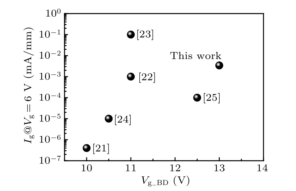
Fig.6. Comparison of gate breakdown voltage and Ig with the previous reported results.
4. Conclusion
AlGaN/GaN heterojunction field-effect transistors(HFETs)with p-GaN cap layer are developed for normally-off operation, in which anin-situ5 nm AlN layer is utilized as gate insulator to further improve the device performance. Owing to the large conduction band offset and band bending of AlN layer, theVthof AlGaN HFETs with p-GaN layer is enhanced to approximately 4 V,and the gate swing is increasing to 13 V.Meanwhile, compared with the normally-off devices by using SiNxas insulator layer,both the forward and reverse gate leakage current are suppressed significantly because of the relatively large conduction band offset. Good device performances are confirmed with a maximum channel electron field-effect mobility closed to 1500 cm2·V?1·s?1.
Acknowledgements
The author Tao-Fei Pu thanks Shenzhen University-Hanshan Normal University Postdoctoral Workstation, for providing the Post-doctoral position and the corporation opportunity with Tokushima University.
Supported by the National Natural Science Foundation of China (Grant No. 61904207), scientific research support foundation for introduced high-level talents of Shenyang Ligong University(Grant No.1010147000914), and the Natural Science Foundation of Sichuan Province, China (Grant No.2022NSFSC0886).
猜你喜歡
Chinese Physics B(2023年11期)2023-12-02 09:23:06
Journal of Donghua University(English Edition)(2023年4期)2023-09-22 14:29:04
羽毛球(2023年6期)2023-06-08 08:04:32
Chinese Physics B(2023年1期)2023-02-20 13:16:40
Plasma Science and Technology(2022年8期)2022-09-14 08:18:00
Chinese Physics B(2022年7期)2022-08-01 06:02:04
意林彩版(2022年2期)2022-05-03 10:23:56
Chinese Physics B(2022年4期)2022-04-12 03:48:20
閱讀(快樂英語高年級)(2017年5期)2017-05-30 10:48:04
都市麗人(2015年4期)2015-03-20 13:33:27

- Chinese Physics B的其它文章
- Fault-tolerant finite-time dynamical consensus of double-integrator multi-agent systems with partial agents subject to synchronous self-sensing function failure
- Nano Ag-enhanced photoelectric conversion efficiency in all-inorganic,hole-transporting-layer-free CsPbIBr2 perovskite solar cells
- Low-voltage soft robots based on carbon nanotube/polymer electrothermal composites
- Parkinsonian oscillations and their suppression by closed-loop deep brain stimulation based on fuzzy concept
- Temperature dependence of spin pumping in YIG/NiO(x)/W multilayer
- Interface effect on superlattice quality and optical properties of InAs/GaSb type-II superlattices grown by molecular beam epitaxy