
Degradation mechanisms for polycrystalline silicon thin-film transistors with a grain boundary in the channel under negative gate bias stress
2022-12-28 09:55:14DongliZhang張冬利MingxiangWang王明湘andHuaishengWang王槐生
Chinese Physics B 2022年12期
關(guān)鍵詞:王明
Dongli Zhang(張冬利), Mingxiang Wang(王明湘), and Huaisheng Wang(王槐生)
School of Electronic and Information Engineering,Soochow University,Suzhou 215006,China
Keywords: negative bias stress,poly-Si,thin-film transistor,grain boundary
1. Introduction
Polycrystalline silicon (poly-Si) thin-film transistors(TFTs)are widely used in pixel circuits and peripheral driver circuits of small-size and high-resolution active-matrix flatpanel displays. However,due to the polycrystalline nature and the existence of grain boundaries(GBs)in the poly-Si film,the electrical characteristics of poly-Si TFTs may be deteriorated depending on the location of the GBs.[1–3]On the contrary,the GB in scaled TFTs is reported to be able to improve the offstate current and the subthreshold swing of poly-Si TFTs.[4]
In addition to the electrical performance of the asfabricated poly-Si TFTs, degradation behavior and the corresponding degradation mechanisms under various kinds of bias stress should be well understood before the optimal design of poly-Si TFTs and TFT-based circuits. Stress conditions,such as positive gate bias stress, negative gate bias stress (NBS),and hot-carrier (HC) effect, could all result into degradation in TFTs’electrical characteristics,but the typical degradation phenomena obviously differ, exhibiting positive[5]and negative shift of the transfer curves[6–8]and decreased on-state current (Ion) with unaffected subthreshold characteristics,[9]respectively.
GB-related HC degradation in poly-Si TFT has been reported,[10]whereas the effects of GB on other kinds of stress-induced degradation are not yet clarified. In the present paper,NBS degradation in poly-Si TFTs with a defective GB in the channel is investigated. Typical NBS degradation with negative shift of the transfer curves is found to be absent. Instead,reduced on-state current,unaffected subthreshold characteristics and suppressed gate-induced drain leakage(GIDL)current are observed. The corresponding mechanisms for the observed degradation phenomena are proposed in this paper.
2. Experiments
TFTs with a defective GB in the channel were fabricated on the basis of metal-induced lateral crystallization (MILC)technology.[11]A 100-nm-amorphous silicon was firstly deposited by the low-pressure chemical vapor deposition on silicon wafers covered with 500-nm thermal oxide. It was then patterned into the active islands before the deposition of 300-nm low-temperature oxide(LTO).After the definition of metal-introducing windows (MIWs) and the following deposition of 10-nm Ni by electron-beam evaporation,MILC heattreatment was carried out in nitrogen atmosphere at 550?C for 24 hrs. Further 24 hrs of post-annealing at 550?C was performed to improve the quality of the poly-Si after removing the unreacted nickel.[12]The TFTs were fabricated on the bilaterally crystallized poly-Si regions, where MIWs were opened on the two ends of the active island and crystallization proceeded from the MIWs towards the center of the active island,as schematically shown in Fig. 1. The two MILC fronts met and formed the defective MILC/MILC GB in the channel region of the TFT, which was perpendicular to the direction of the current flow in the channel.
After the 300-nm covering LTO was removed, the 100-nm LTO was deposited as the gate dielectric and 300-nm poly-Si was deposited and patterned to form the gate, followed by self-aligned phosphorus implantation at a dosage of 4×1015cm?2and an implantation energy of 120 keV.Dopants were activated at 620?C for 3 hrs. A 500-nm LTO was then deposited,through which contact holes were opened,followed by deposition and patterning of 500-nm Al–1%Si into electrode pads. Finally, forming-gas annealing was performed at 420?C for 30 min.
During the application of NBS to the poly-Si TFTs at the room temperature,a constant negative gate bias of?35 V was applied to the gate electrode with the source and drain electrodes grounded. The TFTs’ transfer curves before and after NBS were measured with the semiconductor parameter analyzer Agilent 4156C. The default channel width-tolength ratio of the poly-Si TFTs used in this paper isW/L=10μm/30μm.pendence on drain bias at small drain bias voltages and good saturation phenomenon at high drain bias voltages.
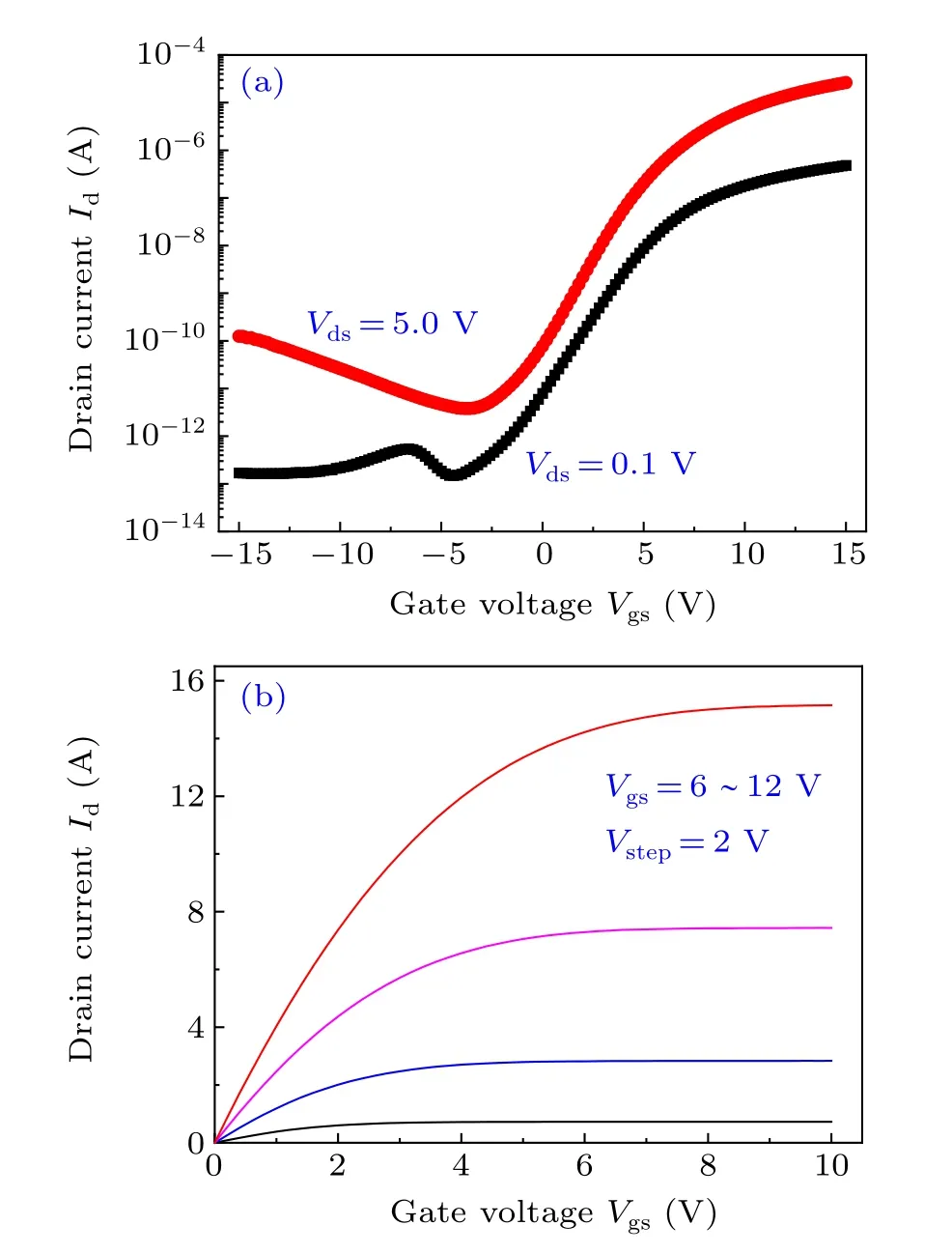
Fig.2. (a)Transfer curves and(b)output curves of the fabricated poly-Si TFTs.
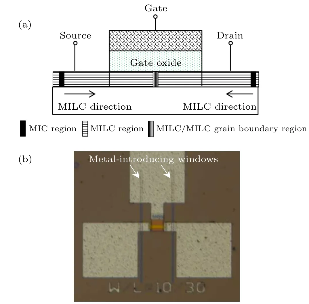
Fig. 1. (a) Cross-sectional diagram and (b) plane-view picture of the TFT with bilaterally crystallized poly-Si channel and one MILC/MILC grain boundary in the channel.
3. Results and discussion
The electrical performance of the fabricated poly-Si TFTs were firstly characterized. Figure 2 shows the representative transfer curves and output curves. From the transfer curve measured withVdsof 0.1 V, the field-effect mobility (μFE),extracted from the maximum transconductance, and threshold voltage(Vth),extracted by the linear extrapolation method,were 85.1 cm2/V·s and 6.5 V, respectively. With an off-sate leakage current (Ioff) of 2.1×10?11A defined as the minimum drain current atVdsof 5.0 V,and on-state current(Ion)of 3.0×10?5A defined as the drain current atVdsof 5.0 V andVgsof 15.0 V,Ion/Ioffis estimated to be 1.43×10⁶. The gate voltage difference characterizing the drain-induced barrier lowing effect(VDIBL)for the same drain current of 1×10?9A atVdsof 0.1 V and 5.0 V is 1.6 V and the subthreshold swing (SS)is 1.45 V/decade. The output curves exhibit good linear de-

Fig.3. Comparison of the transfer curves measured before and after NBS for 7200 s with(a)Vds=5.0 V and(b)Vds=0.1 V.
Figure 3 compares the transfer curves of one poly-Si TFT before and after NBS for 7200 s. The negative shift of the transfer curves frequently observed for poly-Si TFTs under NBS is absent. Instead,the TFT after NBS exhibits decreasedIon, unaffected subthreshold characteristics, and suppressed GIDL current at aVdsof 5.0 V (Fig. 3(a)). These degradation phenomena are quite similar to the typical HC stressinduced degradation phenomena at the first sight. However,the reverse-mode characteristics of the TFT behave almost the same as the forward-mode characteristics (Fig. 4), where the reverse-mode characteristics are measured with the source and drain exchanged from the configurations in forward-mode measurements. While the on-state current degrades more under reverse mode than under forward mode in HC-induced degradation.[13]
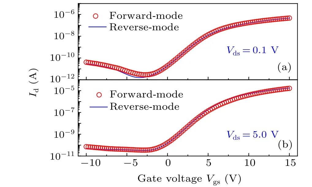
Fig.4. Comparison of the transfer curves measured in forward mode and reverse mode for poly-Si TFT under NBS for 7200 s with(a)Vds=0.1 V and(b)Vds=5.0 V.
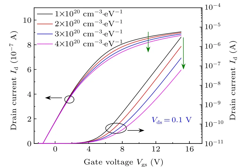
Fig. 5. Simulated transfer characteristic curves for poly-Si TFTs with different nTA values in the grain boundary.
The decreased on-state current after NBS indicates the trap state generation and the unaffected subthreshold characteristics imply that the trap states are not produced uniformly in the channel region.[14,15]Further considering the existence of weak Si–Si bonds and Si–H bonds in the GB,the trap states are most probably locally generated in the MILC/MILC GB.The hypothesis that the locally increased trap states in the GB result into the decreased on-state current were verified by simulation with Silvaco Atlas,[16]where the GB region was set to be 1 μm wide and the concentration of the acceptor-like tail states (nTA) was increased after fitting the initial transfer curves. The parameters, including the distribution of trap states in the poly-Si outside the GB and in the GB, are summarized in Tables 1 and 2,respectively.
As shown in Fig. 5, the on-state current dose decreases with the increase innTA. The energy barrier in the conduction band formed at the GB in the on-state withVgsof 15 V increases with the increase innTA(Fig. 6) which couldhinder the current flow and suppress the on-state current. Furthermore, when thenTAin the GB region is increased to 4.2×1020cm?3·eV?1and thenGA,the peak value of acceptorlike deep states, is increased to 1.2×1018cm?3·eV?1, the measured subthreshold and on-sate characteristics after NBS for 7200 s could be well fitted by the simulated results(Fig.7),thereby confirming the validity of the proposed mechanism.
Table 1. Parameters for the poly-Si outside the GB region.
Table 2. Parameters for the poly-Si in the GB region.

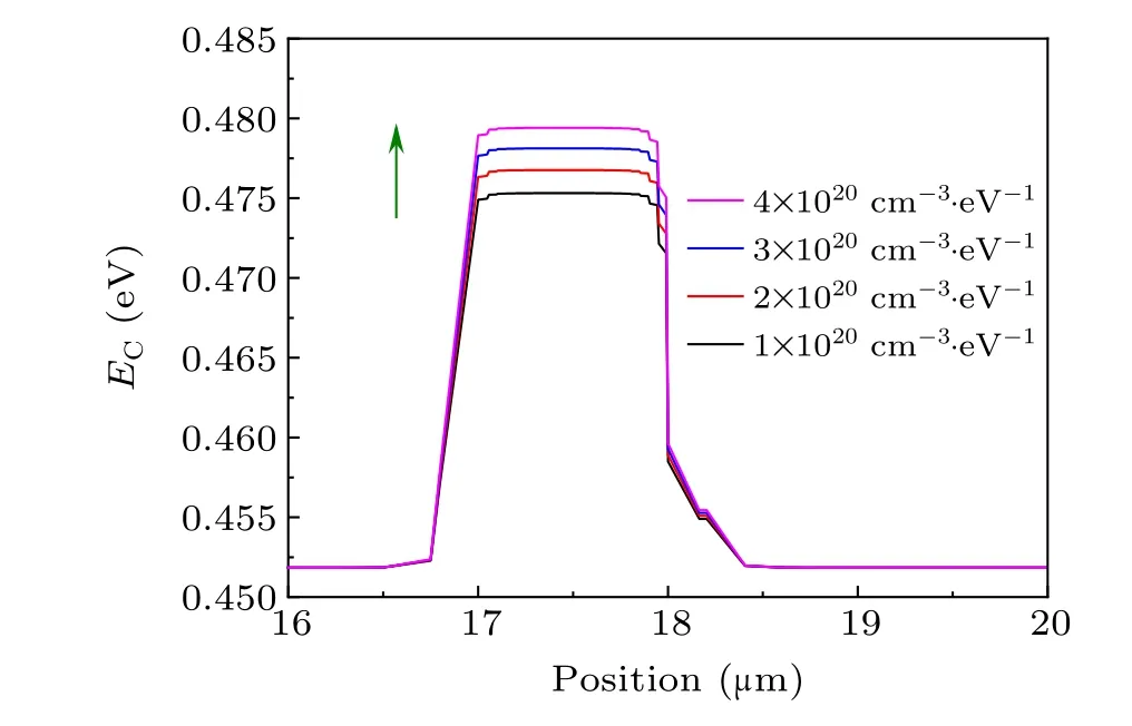
Fig.6. Comparison of the energy barrier for electrons in the conduction band formed at the grain boundary with different nTa,where Vgs is 15 V and Vds=0 V.
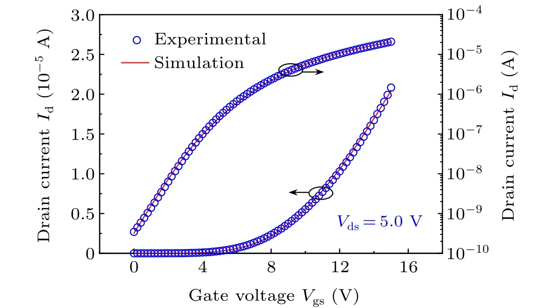
Fig.7. Comparison of the transfer curve measured with Vds=5.0 V after NBS for 7200 s and that simulated with nTA=4.2×1020 cm?3·eV?1 and nGA=1.2×1018 cm?3·eV?1 in the grain boundary.
In the NBS degradation mechanism, the holes available in the active layer are important factors to trigger the reactions in the NBS degradation and generation of positive charges in the gate oxide.[17–19]So, the 2D distribution contour of hole concentration in the active layer under the stress gate bias of?35 V was simulated. As shown in Fig.8,high-concentration holes appear at the front surface in the GB and outside the GB regions.
Vertical distributions of the holes in the GB and those outside the GB were firstly extracted and compared (Fig. 9).At the top surface, the hole concentration is as high as 1.0×1019cm?3and 5.8×1018cm?3for the poly-Si outside the GB and in the GB regions, respectively. For a position far from the surface and at the same depth,the hole concentration in the GB is also much smaller than that outside the GB due to the higher trap state density in the GB.The lateral distribution of the holes in the channel at a depth of 80 nm from the top surface of the active island was also extracted,as shown in Fig.10. The hole’s concentration shows a peak value near the source/drain junctions and the peak concentration is surprisingly found to be more than two orders of magnitude higher than that in the active layer far from the source/drain junctions.
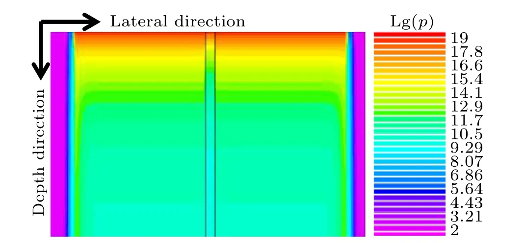
Fig. 8. Simulated 2D distribution contour of holes in cross-section of the active layer with a gate bias of ?35 V.
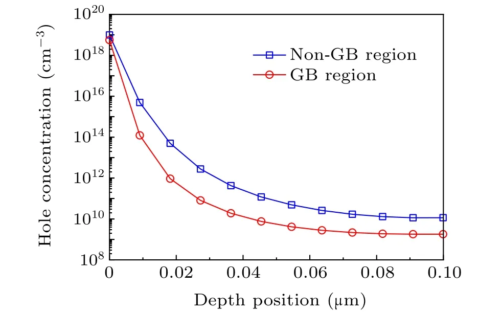
Fig.9. Depth distribution of holes in the GB and outside the GB region with a gate bias of ?35 V.
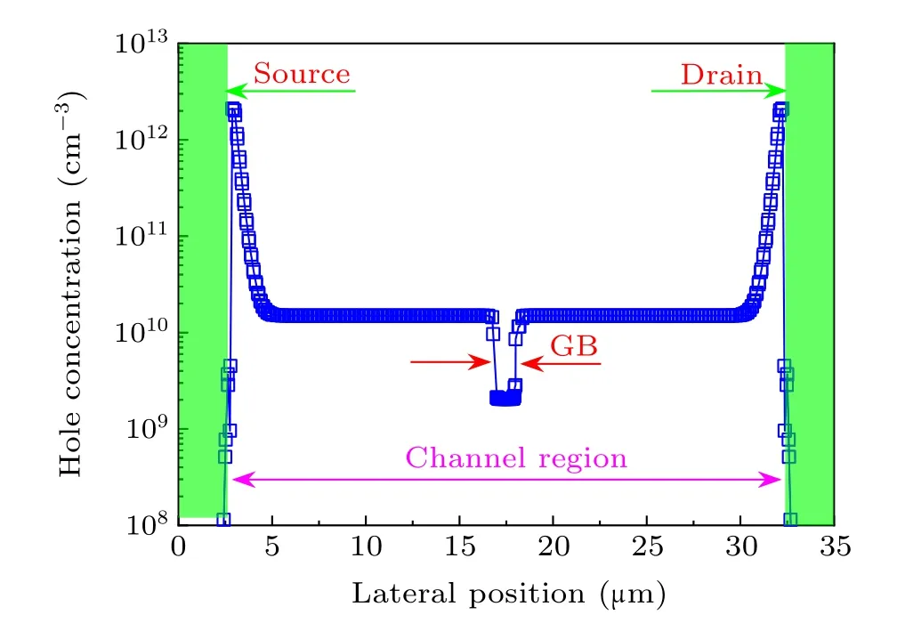
Fig.10. Simulated lateral distribution of holes in the active island at a depth position of 80 nm with a gate bias of ?35 V.
During NBS,the potential of the channel is coupled to be negative in respect to the grounded n+source and drain. Thus,reversely biased pn junctions are formed. The generated carriers in the depletion region of the source/drain pn junctions are separated by the electric field and holes drift into the channel of the TFT.In the neutral channel region,the holes diffuse towards the channel center from the source and drain sides,accompanied by recombination in the channel simultaneously.Then,a non-uniform distribution of holes in the channel could be observed.[20]
The validity of the proposed explanation on the nonuniform distribution of holes in the active layer was further verified,where the lifetime of holes was varied. As shown in Figs.11(b)and 11(c),the peak concentration and the distribution range of the peak for holes near the source/drain decrease as the lifetime of holes decreases. When the carrier generation in the source/drain depletion region through trap-assisted tunneling is further excluded, which is accounted for the fitting of the GIDL current during the simulation of initial transfer curves, the holes distribute uniformly in the channel and the concentration is as low as 1.5×1010cm?3[Fig.11(d)],which is also reasonable as the thermal generation of holes in the active layer is uniform.
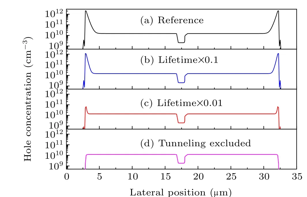
Fig.11.Comparison of the simulated lateral distribution of the hole at a depth position of 80 nm in the active island with(a)default parameters,(b)lifetime reduced by one order of magnitude, (c) lifetime reduced by two orders of magnitude,and(d)carrier tunneling model excluded during simulation.
Considering the higher-concentration holes in the channel near the source and drain under NBS,typical NBS degradation still takes place with positive charges(Qox)formed locally in the gate oxide near the source and drain. The locally distributed positive changes screen the electric field from the gate in the off-state and reduce the GIDL current, such that the dependence of leakage current on gate bias atVdsof 5.0 V is greatly reduced, as observed in Fig. 3(a).[21]As shown in Fig.12,the suppression effect of the GIDL current after NBS could be achieved by adding positive charges in the gate oxide in 0.5-μm-long regions from the gate edges,and the suppression effect is more effective with the increase in locally distributed positive charges in the gate oxide. For example,with aQoxof 4.0×1017cm?3, the GIDL current is suppressed to a current level of 5.8×10?11A, which is very close to the measured current of 6.5×10?11A after NBS.
Figure 3(b)shows that the leakage current atVdsof 0.1 V,which is initially thermal generation dominated and gate-bias independent,significantly increases and becomes gate-bias dependent after NBS. Figure 13 compares the drain current,source current (Is), and gate leakage current (Ig) in the offstate atVdsof 0.1 V after NBS for 7200 s. The drain current and the source current show gate-bias dependence, and the dependence trend is similar to that for the gate leakage current. The sum of drain current and source current equals to the gate leakage current in the off-state. Thus,after NBS,the drain current atVdsof 0.1 V is clearly dominated by the gate leakage current. Considering that the gate leakage current before NBS shows gate-bias independence and as low as 0.1 pA(Fig.13),the defect-related conduction path in the gate oxide could be concluded to be introduced during NBS,such that the gate leakage becomes larger than the generation current at the drain junction and dominates the drain current at smallVds.
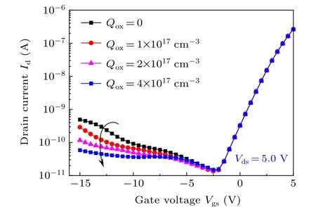
Fig. 12. Suppressed GIDL current in the simulated transfer curves with different Qox values added in the gate oxide near the source and drain.
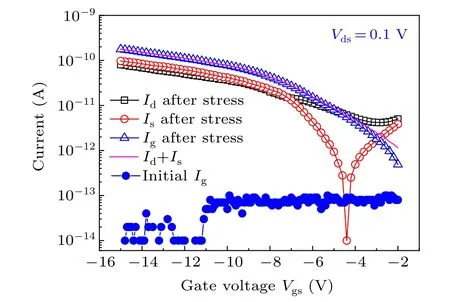
Fig. 13. Comparison of the drain current, source current, and gate leakage current after NBS.The initial gate leakage current before NBS is also shown as a reference.
4. Conclusion
NBS degradation phenomena featured with reduced onstate and GIDL but increased gate bias dependence of the leakage current atVdsof 0.1 V are observed for poly-Si TFTs with a defective GB in the channel. Trap state generation in the GB, local generation of positive charge in the gate oxide near the source/drain,and trap state generation in the gate oxide are proposed to be the respective causes for the observed phenomena. The high-concentration holes in the bulk of the active island near the source/drain junctions are responsible for the local generation of positive charges in the gate oxide which suppresses the GIDL current.Meanwhile,the low concentration of holes in the bulk of the active island far from the source/drain junctions is proposed to the reason for the absence of the shift of the transfer curve after NBS.
Acknowledgments
Project supported by the National Natural Science Foundation of China (Grant Nos. 61971299 and 61974101), the Natural Science Foundation of Jiangsu Province of China(Grant No.BK20201201),the Fund from Suzhou Science and Technology Bureau (Grant No. SYG201933), and the Fund from the State Key Laboratory of ASIC and System, Fudan University(Grant No.2021KF005).
猜你喜歡
Chinese Physics B(2023年12期)2023-12-15 11:51:14
Chinese Physics B(2022年8期)2022-08-31 09:59:36
應(yīng)用數(shù)學(xué)(2022年3期)2022-07-07 07:37:14
Chinese Physics B(2021年11期)2021-11-23 07:32:04
北方音樂(2019年10期)2019-07-10 19:13:36
北方音樂(2019年10期)2019-07-10 19:13:36
海峽姐妹(2019年3期)2019-06-18 10:37:22
金色年華(2017年2期)2017-06-15 20:28:30
Acta Mathematica Scientia(English Series)(2015年5期)2015-11-21 07:11:55
棋藝(2014年1期)2014-05-20 02:07:43

- Chinese Physics B的其它文章
- Fault-tolerant finite-time dynamical consensus of double-integrator multi-agent systems with partial agents subject to synchronous self-sensing function failure
- Nano Ag-enhanced photoelectric conversion efficiency in all-inorganic,hole-transporting-layer-free CsPbIBr2 perovskite solar cells
- Low-voltage soft robots based on carbon nanotube/polymer electrothermal composites
- Parkinsonian oscillations and their suppression by closed-loop deep brain stimulation based on fuzzy concept
- Temperature dependence of spin pumping in YIG/NiO(x)/W multilayer
- Interface effect on superlattice quality and optical properties of InAs/GaSb type-II superlattices grown by molecular beam epitaxy