
Degradation mechanisms for a-InGaZnO thin-film transistors functioning under simultaneous DC gate and drain biases
2022-08-31 09:59:36TianyuanSong宋天源DongliZhang張冬利MingxiangWang王明湘andQiShan單奇
Chinese Physics B 2022年8期
關(guān)鍵詞:王明
Tianyuan Song(宋天源) Dongli Zhang(張冬利) Mingxiang Wang(王明湘) and Qi Shan(單奇)
1School of Electronic and Information Engineering,Soochow University,Suzhou 215006,China
2Visionox Technology Co.,Ltd,Suzhou 215006,China
Keywords: a-IGZO,thin-film transistors,hot-carrier effects
1. Introduction
Amorphous InGaZnO (a-IGZO) thin-film transistors(TFTs)are a promising technology for large-size active-matrix displays owing to their low processing temperature,low leakage current, high uniformity, and relatively high mobility.[1]However, as a switch in the actual work scenario, TFTs are turned on by a gate bias,and then the storage capacitors connected in series will be charged up when a drain bias is applied.The frequent charging processes make the TFTs subjected to a continuous large voltage stress, and the resulting degradation of electrical characteristics of the switch TFTs will seriously affect the quality of the display. Therefore, research on reliability issues of a-IGZO TFTs under simultaneous bias stress appears extremely important.
Previous studies on the reliability of a-IGZO TFTs under bias stress include positive gate bias stress(PBS)and negative gate bias stress (NBS). The positive shift of the characteristic transfer curves of a-IGZO TFTs under PBS has been attributed to carrier trapping in the bulk active layer or at the active layer/gate insulator interface.[2,3]NBS in dark conditions has a negligible effect, but when combined with light illumination (NBIS), large negative threshold voltage shifts are induced,and NBIS has been attributed to defect creation and/or hole trapping at the active-layer/gate-insulator interface.[4–6]In most situations,however,a drain bias is also applied simultaneously with the gate bias. If the gate and drain biases are large,a high current may flow through the TFT and result into joule heating of the TFT’s active layer.[7–10]
In this study, the reliability of a-IGZO TFTs under simultaneous gate and drain bias stress is systematically investigated. The degradation mechanism is proposed to be hot electrons trapping in the etching-stop layer (ESL), while the self-heating effect is negligible. The maximum degradation occurs under the bias stress condition in which both the electric field and electron concentration are relatively high at the same time. A larger drain voltage can significantly reduce the potential barrier formed by electrons trapped in the ESL and make the a-IGZO TFT function properly.
2. Experiments
The cross-sectional view of the a-IGZO TFTs used in this study is shown in Fig.1. A 150-nm-thick molybdenum(Mo)was first deposited and patterned to form the gate. Then,100-nm-thick SiO2was deposited at 300?C via plasma-enhanced chemical vapor deposition(PECVD)as the gate dielectric. A 50-nm a-IGZO was deposited at 150?C by sputtering with Ar mixed with 6% O2and annealed in dry air at 350?C for 1 hour. After the a-IGZO was patterned into active islands,50-nm PECVD SiO2was deposited at 150?C and patterned as the ESL.A 150-nm-thick Mo was deposited and etched to form source/drain electrodes. After the electrodes were defined,a passivation layer of 300-nm SiO2was deposited. The source/drain electrodes extending over the ESL formed the extended source electrode (ESE) and the extended drain electrode(EDE)regions,as labeled in Fig.1,where the length of ESE(LESE)and the length of EDE(LEDE)are the same.
For the default bias stress condition, a DC bias of 25 V is applied to the gate, and a simultaneous bias stress of 30 V is applied to the drain with the source grounded. The channel width-to-length ratio of a-IGZO TFTs is 10 μm/20 μm. Device degradation is characterized by the change of the turn-on voltage(Von)and threshold voltages(Vth)from their respective initial values, whereVonis defined as the gate voltage corresponding toID=10?10A,Vth1andVth2are extracted by the linear extrapolation method from the first and second linear regions of the transfer curve on a linear scale,which is measured withVdsof 0.1 V.
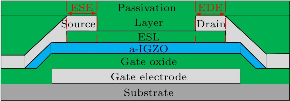
Fig.1. Schematic cross-sectional diagram of the a-IGZO TFT.
3. Results and discussion
Figure 2 shows the evolution of the transfer curve of the a-IGZO TFT under the stress condition withVgs=25 V andVds=30 V, where current distortion appears when the drain current transients from the subthreshold region to the on-state region and the subthreshold current exhibits a parallel positive shift without a change in the subthreshold swing, indicating that trap state generation is negligible and the degradation is caused by electron trapping.[3]Correspondingly, the on-state current shows a two-slope dependence on the gate bias in addition to the positive shift of the on-state current. ?Von,?Vth1,and ?Vth2of the a-IGZO TFT after the stress are compared in Fig. 3. Note that ?Vonis almost equal to ?Vth1and larger than ?Vth2. For example,after 3000 s stress time,?Von,?Vth1,and ?Vth2are 15.2 V, 15.3 V, and 14.0 V, respectively. The difference in the degradation of the subthreshold current and the on-state current indicates that electron injection occurs in a local region in the gate oxide or the ESL. The logarithmic relationship between the variations inVon,Vth1, andVth2and stress time indicates that a similar degradation mechanism is involved.
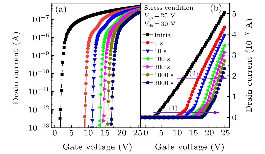
Fig. 2. Evolutions of the transfer curve measured at Vds =0.1 V for the a-IGZO TFTs on (a) logarithmic scale and (b) linear scale under the stress conditions of Vgs=25 V and Vds=30 V.
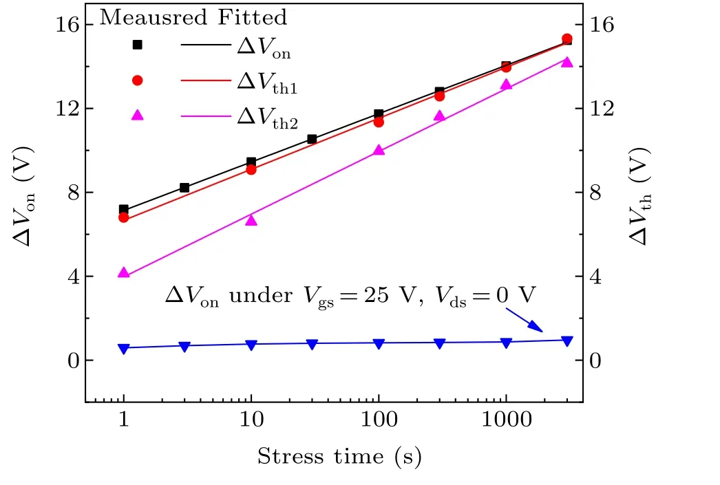
Fig.3. Comparison of ?Von,?Vth1,and ?Vth2 of the a-IGZO TFT under bias stresses of Vgs =25 V and Vds =30 V and ?Von under gate bias stresses of Vgs =25 V and Vds =0 V.The fitting lines for the dependence of the variations in Von,Vth1,and Vth2 on stress time are added.
After fitting the initial transfer curves of the a-IGZO TFT with the Silvaco Atlas,density of states(DOS)in the channel a-IGZO is extracted and summarized in Table 1. Distributions of the vertical electric field (Evert) and electron concentration(ne)in the a-IGZO withVgs=25 V andVds=30 V were then extracted. As shown in Fig. 4(a), the vertical electric field is strong at the back channel interface below the EDE region and at the front channel interface outside the EDE region, where the electric fields are 1.85×10⁵V/cm and 1.19×10⁵V/cm,respectively. For the distribution of electrons, as figure 4(b)shows,electrons also accumulate both at the back channel under the EDE region and at the front channel outside the EDE region,where the electron concentrations are 9.6×1018cm?3and 3.7×1018cm?3, respectively. Therefore, electron trapping during the bias stress could occur at both the back channel under the EDE region and the front channel outside the EDE region.
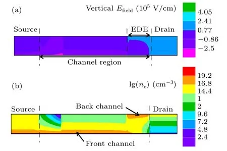
Fig.4. Distributions of(a)vertical electric field and(b)electrons in a fresh a-IGZO TFT when Vgs=25 V and Vds=30 V.
However, when a positive gate bias stress withVgsof 25 V and grounded source/drain was applied,which produces the same electron concentration and electric field in the front channel as those outside the EDE region underVgs=25 V andVds=30 V,?Vonis smaller than 0.96 V,as shown in Fig.3,indicating that electron trapping in the gate oxide is minimal,probably due to the good quality of the gate oxide, which limits the tunneling of electrons into the gate oxide.[11]Thus,the observed degradation under the simultaneous DC gate and drain biases is attributed to that occurring at the back channel under the EDE region.
To further clarify the degradation mechanism, the gate bias during the bias stress is decreased. As shown in Fig.5(a),?Vonincreases first and then decreases with the decrease of the gate bias, reaching a peak value atVgsof 7 V.The maximum degradation of the a-IGZO TFT occurs whenVgsis relatively small rather than when bothVgsandVdsare relatively large at the same time,indicating that the degradation is not dominated by the self-heating effect due to the Joule heat generated by the drain current and drain voltage.[12]
The increased temperature(?T)in the a-IGZO TFT during the bias stress withVgs=25 V andVds=30 V is estimated through the following formula

whereLis 350 nm, which is the sum of the thickness of the ESL and passivation layer;λis 1.3, which is the coefficient of the thermal conductivity of SiO2;andSis the heat dissipation area and is estimated by the product ofW(10 μm) andL(20 μm).Pheatis estimated as 1.88 mW by the production of the drain voltage and the drain current of one fresh TFT.The increase in the temperature of the a-IGZO channel during bias stress is as small as 2.4?C. Therefore, the effect of the heat generation during the bias stress on the degradation of a-IGZO TFTs is negligible.

Table 1. Parameters for the distribution of trap states for the simulation of the initial transfer curve of a-IGZO TFT.
From the simulation results in Fig.5(b),the electron concentration at the back channel surface under the EDE region first increases quickly and then gradually asVgsincreases.In contrast, the vertical electric field is continuously reduced whenVgsincreases. Under stresses ofVgs=25 V andVds=30 V,there is a high electron concentration but a low vertical electric field. In contrast, there is a small electron concentration but a high vertical electric field whenVgsis 0 V and 3 V.The gate bias of 7 V,which is slightly higher than the threshold voltage,provides both a relatively high electron concentration and electric field at the same time and induces maximum degradation of the a-IGZO TFT, which is a typical condition under which hot-carrier effects occur.
The ?Vonafter bias stresses with differentVdsare compared in Fig.6,and a logarithmic time dependence is observed.The relationship between ?Vonand stress time was fitted with?Von=rdlog(t/τ0),[13]whererdis a function of the tunneling constant andτ0is the characteristic time. The logarithmic dependence on stress time indicates that the electrons were tunneled into and trapped in the ESL near the interface and did not redistribute further after being trapped.[13–16]The dependence of ?Vthon stress time in Fig. 3 can also be fitted with the logarithmic relationship,indicating that the same degradation mechanism is involved for the subthreshold current and on-state current.

Fig. 5. (a) Effects of Vgs during bias stress with Vds of 30 V on ?Von after 3000-s stress time; (b)simulated Evert and ne at back channel surface under EDE region when bias stresses with different Vgs are applied.
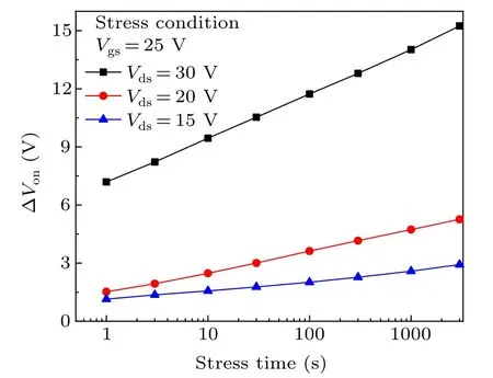
Fig.6. Comparison of ?Von under bias stress condition with Vgs of 25 V but different Vds.
Figure 7 shows the transfer curves measured at different drain biases after the a-IGZO TFT was stressed for 3000 s underVgs=25 V andVds=30 V. Obviously, it can be seen that the drain bias during the measurement of the transfer curve affects the amount of the positive shift of the transfer curve. The electron trapped in the ESL under the EDE region induces a potential barrier with a height of 3.55 eV whenVds=0.1 V, as shown in Fig. 8, where electrons with a density of 2.15×1018cm?3are added in 10-nm regions in the ESL under the EDE region to account for the positive shift of the transfer curve. The potential barrier hinders the current flowing to the drain through the back surface of the a-IGZO under the EDE region. However,it is effectively lowered by a drain voltage higher than 10 V,and the current in the a-IGZO channel can flow freely from the source region to the drain region through the back surface of the a-IGZO under the EDE region, as in the fresh TFT, so the observed degradation,i.e.,the positive shift of the transfer curve,becomes minimal.
Figure 9 compares the output curves for the a-IGZO TFT before and after a bias stress ofVgs=25 V andVds=30 V.Current crowding appeared after the stress,and the current started to increase only whenVdswas larger than 5 V, which means that electrons could not drift freely from the source electrode to the drain electrode in the degraded TFT.[17]This is consistent with the potential barrier formed under the EDE region at the drain side owing to electron trapping after bias stress,which cannot be lowered under a small drain voltage and hinders the flow of electrons in the channel to the drain electrode.As shown in Fig. 9(a), current crowding also appeared in the output curves whenVdswas close to 0 V for a fresh TFT,which can also be explained by the same mechanism as electron trapping in the ESL under the EDE region during the measurement of the output characteristic curves.

Fig. 7. Comparison of the transfer curves measured at different drain biases for the a-IGZO TFTs after 3000-s stress time under Vgs =25 V and Vds=30 V.
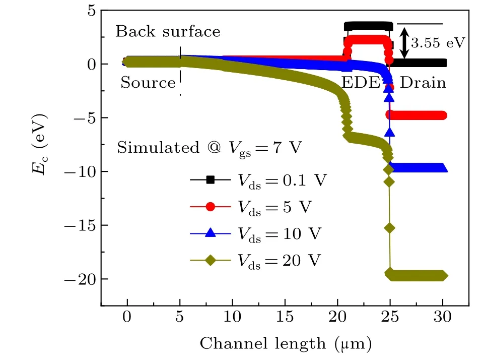
Fig. 8. Comparison of the conduction band at the back a-IGZO surface at different Vds for the a-IGZO TFT after 3000-s stress time under Vgs =25 V and Vds=30 V.
As shown in Fig. 10(a), electrons can accumulate in the front channel outside the EDE region with a smallVgsof 5 V after 100-s stress time under the default stress condition.However,the channel and accumulated electrons at the back channel under the EDE region disappeared when electrons with a density of 1.6×1018cm?3are added to the 10-nm regions in the ESL under the EDE region to account for the positive shift of the transfer curve after 100 s under the default stress condition. The trapped electrons in the ESL under the EDE region increase the potential barrier of the a-IGZO channel under the EDE region, thereby increasing the threshold voltage of the parasitic TFT in the drain electrode region. In Fig.10(b),one can notice that electrons can flow to the drain only when the gate bias is high enough to accumulate electrons in the front channel under the EDE and form the conduction path. Thus,the current crowding phenomena in the output curves starts at a smaller drain bias at a higher gate bias as shown in the Fig. 9. Therefore, the subthreshold current in Fig. 2(a) and the first linear dependence of the drain current on the gate bias in Fig. 2(b) are due to channel formation and current flow in the a-IGZO region outside the EDE region,where the channel length is long. The second linear dependence of the drain current on the gate bias in Fig.2(b)is dominated by conduction in the channel formed under the EDE region when the gate bias is high enough,where the channel length is short.
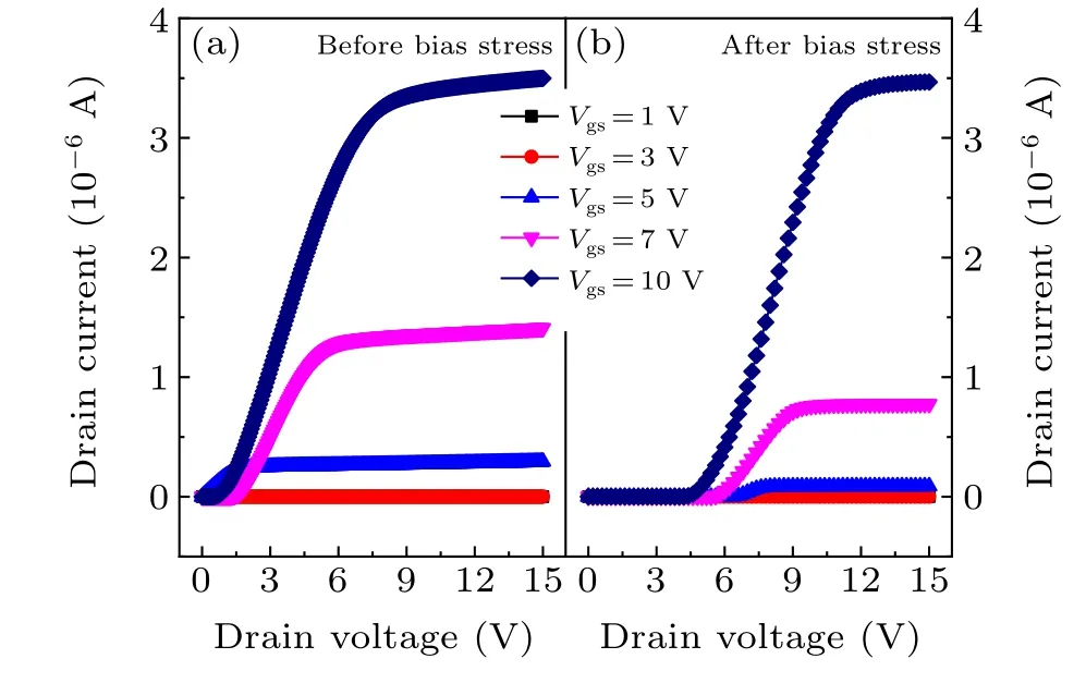
Fig.9. Evolutions of the output curves for the a-IGZO TFTs(a)before and(b)after bias stresses of Vgs=25 V and Vds=30 V.

Fig. 10. Distribution of electrons in the a-IGZO at (a) Vds = 0.1 V and Vgs =5 V and (b) Vds =0.1 V and Vgs =25 V, which is extracted for the TFTs after the default stress for 100 s.
As the tunneling of electrons into the ESL is the critical process during the degradation of the a-IGZO TFTs under the simultaneous DC gate and drain bias stress,the stability of the a-IGZO TFT can be enhanced by reducing the electric filed in the ESL under the EDE region,which can be achieved by either make the a-IGZO under the EDE region conductive[18]or increase the thickness of the ESL.
4. Conclusion
The a-IGZO TFTs with an ESL structure exhibit a positive shift of the transfer curve and two-slope dependence of the drain current on the gate bias after a simultaneous DC gate and drain bias stress. The degradation is proven to be a hot-carrier effect degradation and occurs locally in the back channel under the EDE region. Electron trapping in the ESL under the EDE region and the corresponding potential barrier formed in the back surface of channel a-IGZO successfully explained the observed degradation phenomena in both the transfer and output curves.
Acknowledgments
Project supported by the National Natural Science Foundation of China (Grant Nos. 61971299 and 61974101), the Natural Science Foundation of Jiangsu Province of China(Grant No.BK20201201),the Fund from Suzhou Science and Technology Bureau (Grant No. SYG201933), and the Fund from the State Key Laboratory of ASIC and System, Fudan University,(Grant No.2021KF005).
猜你喜歡
Chinese Physics B(2023年12期)2023-12-15 11:51:14
Chinese Physics B(2022年12期)2022-12-28 09:55:14
應用數(shù)學(2022年3期)2022-07-07 07:37:14
Chinese Physics B(2021年11期)2021-11-23 07:32:04
北方音樂(2019年10期)2019-07-10 19:13:36
北方音樂(2019年10期)2019-07-10 19:13:36
海峽姐妹(2019年3期)2019-06-18 10:37:22
Acta Mathematica Scientia(English Series)(2015年5期)2015-11-21 07:11:55
棋藝(2014年1期)2014-05-20 02:07:43
Chinese Journal of Chemical Engineering(2014年2期)2014-03-25 09:11:23

- Chinese Physics B的其它文章
- Magnetic properties of oxides and silicon single crystals
- Non-universal Fermi polaron in quasi two-dimensional quantum gases
- Purification in entanglement distribution with deep quantum neural network
- New insight into the mechanism of DNA polymerase I revealed by single-molecule FRET studies of Klenow fragment
- A 4×4 metal-semiconductor-metal rectangular deep-ultraviolet detector array of Ga2O3 photoconductor with high photo response
- Wake-up effect in Hf0.4Zr0.6O2 ferroelectric thin-film capacitors under a cycling electric field