
Influence of the lattice parameter of the AlN buffer layer on the stress state of GaN film grown on(111)Si
2023-03-13 09:20:12ZhenZhuoZhang張臻琢JingYang楊靜DeGangZhao趙德剛FengLiang梁鋒PingChen陳平andZongShunLiu劉宗順
Chinese Physics B 2023年2期
Zhen-Zhuo Zhang(張臻琢) Jing Yang(楊靜) De-Gang Zhao(趙德剛) Feng Liang(梁鋒)Ping Chen(陳平) and Zong-Shun Liu(劉宗順)
1State Key Laboratory of Integrated Optoelectronics,Institute of Semiconductor,Chinese Academy of Sciences,Beijing 100083,China
2College of Materials Science and Opto-Electronic Technology,University of Chinese Academy of Sciences,Beijing 100049,China
3Center of Materials Science and Optoelectronics Engineering,University of Chinese Academy of Sciences,Beijing 100049,China
Keywords: GaN,Si substrate,AlN buffer layer,stress control
1.Introduction
As a wide band gap semiconductor,GaN is attracting increasing attention in microelectronics and optoelectronics devices, such as high electron mobility transistors (HEMT),[1]light emitting diodes(LED),[2]and laser diodes(LD).[3]Compared to sapphire, SiC and GaN, using Si as the substrate is expected to reduce costs and achieve integration.Unfortunately, the reaction between Ga and Si, namely, the meltback etching effect, and the large mismatch in lattice constants (17%) and thermal expansion coefficients (56%) between Si and GaN severely restrict the development of GaNon-Si growth technology.[4]Choosing AlN instead of GaN as the material of the buffer layer is an effective way to isolate Ga atoms from Si and thus avoid melt-back etching.[5]To solve the mismatch in the coefficient of thermal expansion (CTE)and reduce the high density of threading dislocations (TDD)causing by the large lattice mismatch, several methods were used to enhance compressive stress to compensate the tensile stress generated during the cooling process and also to reduce the threading dislocations during the growth process, such as using a multiple AlGaN intermediate layer,[6]low temperature AlN (LT-AlN) insert layer,[7]AlGaN/GaN superlattice buffer layer[8]and so on.Nevertheless,these techniques have to introduce additional layers into the system,and the complicated techniques would reduce device reliability and would not be conducive to cost reduction,[9]which is one of the original purposes of GaN-on-Si growth technology.
A GaN/AlN heterostructure interface can introduce a theoretically large enough compressive stress in both the growth process and cooling process due to the smaller lattice parameter and smaller thermal expansion coefficient of AlN compared to GaN.[10]However,it is known that the growth mode of the AlN buffer layer on Si is normally the Vollmer-Weber mode and its initial stage is nucleation and island coalescence.[11]A high TDD will be unavoidably formed in the AlN buffer layer during the coalescence of island boundaries.[12]Due to the high TDD in the AlN buffer layer, the compressive stress relaxes and transforms to tensile stress due to the low quality AlN buffer layer[13,14]and thus an ideal result cannot be achieved.
Nowadays, with deepening understanding of AlN crystal growth, a higher quality AlN buffer layer can be achieved.[15,16]Therefore, the hope of using a simple buffer layer structure to realize crack-free GaN-on-Si has been rekindled again in recent years.[16-24]In this field, some teams focus on optimizing TMA[20,21]or ammonia[22,23]preflow conditions or AlN buffer layer design by modifying the temperature[12,16,25]to further improve the quality of the AlN buffer layer, and thus increase the compressive stress applied to GaN and achieve thicker crack-free GaN-on-Si with a low density of threading dislocations.However, due to the huge lattice mismatch between AlN and Si(19%),the thickness of AlN is limited to several hundred nanometers,[16]which also limits the further improvement of the quality of the AlN buffer layer.[26]Thus, improving the quality of the AlN buffer layer is not easy,and additional measures need to be found.
In this work,it is found that the in-plane stress at the initial stage of GaN growth is sensitive to the lattice parameter of the AlN buffer layer.The results of further orthogonal experiments show that the most important factor affecting the lattice parameter of the AlN buffer layer is its growth rate.By optimizing the lattice parameter of the AlN buffer layer,a 0.8μm thick GaN film without cracks(except the edge zone)and with full widths at half maximum(FWHM)for(002)and(102) x-ray diffraction (XRD) rocking curves of 717 arcsec and 838 arcsec,respectively,are achieved.
2.Experiment
AlN and GaN were all grown on a 2-inch (111) Si substrate by an Aixtron 6×2 inch close-coupled showerhead reactor metal-organic chemical vapor deposition (MOCVD)system.The (111) Si substrate wafer used in the MOCVD growth was prepared by the floating-zone technique and was epi-ready.The resistivity of the substrate was higher than 1000 Ω·cm.Due to the vacuum package and the N2atmosphere in the glove box,no additional cleaning procedure was needed before the Si wafer was moved into the reaction chamber.Trimethygallium(TMG),trimethylaluminum(TMA),and ammonia (NH3) were used as the Ga, Al and N sources, and H2and N2were used as carrier gases.The Si substrate was baked at~1050°C in a H2atmosphere for 5 min to remove the native surface oxidation layer.Then,TMA was introduced in the reactor to prevent the formation of amorphous SixNydue to the possible reaction between the Si substrate and residual ammonia in the reactor.Subsequently, ammonia was introduced into the reactor and an AlN buffer layer with a thickness of 200 nm was grown.The main growth parameter variables of these three samples are listed in Table 1.Other parameters except those listed in Table 1,such as the thickness of the AlN buffer layer, V/III mole ratio and so on, were kept constant(the growth rate was controlled by modifying the flow rates of MO sources and ammonia).After the growth of AlN,0.8μm GaN films were grown at 1050°C on the AlN buffer layer under the same condition.The reactor pressures of AlN and GaN growth were 100 mbar and 260 mbar,respectively.

Table 1.Main growth conditions of the AlN buffer layers for samples A,B,and C.
Thein-situcurvature of the samples was monitored during MOCVD growth by Lay-tec EpiCurve?TT software.The Raman spectra of the three samples were measured at room temperature by 532 nm laser excitation.The FWHM of the rocking curves were measured by triple-axis high resolution x-ray diffraction(HRXRD).HRXRD was performed employing a CuKα1line of wavelengthλ=0.15406 nm.The surface morphology was examined by a Normaski microscope and atomic force microscope(AFM).
3.Results and discussion
Thein-situcurvature curves measured during the GaN layer growth of samples A, B and C are plotted in Fig.1.The mean stress during the epitaxy process at growth temperature can be deduced from the slope of the curve according to Stoney’s formula[14]
whereσmis the mean stress applied to the film,Esis the Young modulus of the substrate and equals 1.85×10¹¹N/m2for Si,[27]νsis the Poisson ratio of the substrate and equals 0.26,[27]hsis the thickness of the Si substrate and equals 430 μm,hfis the thickness of the grown film, andκis the measured curvature.

Fig.1. In-situ curvature value versus time for the growth of three GaN films on different AlN buffer layers.The solid curves are the ones recorded during the measurement where the additional undulations are a normal phenomenon caused by optical interference.The dotted curves are plotted after smoothing treatment of the original data.These curves show only their patterns but not the calibrated value of curvature.
After a calibration treatment and differentiating, the initial stress of the interface between AlN and GaN is calculated as-0.432 GPa,-0.955 GPa, and-1.359 GPa, where the negative sign represents that the stress is compressive.The fact that the absolute value of the slope gradually decreases indicates the relaxation of compressive stress.It can be seen that the compressive stresses in the three samples do not completely transform to tensile stress during the growth of 0.8μm thick GaN film, indicating the high quality of the AlN buffer layers.[13,14]
Figure 2 shows the HRXRDω-2θscan diffraction patterns of the samples.The typical results of triple-axisω-2θscans from Si(111), GaN(002),AlN(002),GaN(004), and AlN(004)reflection are marked in Fig.2(a).In order to confirm the lattice constant from theω-2θscans, scanning with high precision was done near the peak positions of GaN(004)and AlN(004).The lattice parameters can be calculated by Bragg’s law[28]
whered⊥is thec-plane lattice parameter actually measured,nis the diffraction order,which equals 4 in this experiment,andλis the wavelength of the x-rays, which equals 0.15406 nm.The step length of the scanning is 0.0001°and the error can be obtained by differentiating Bragg’s law to give[28]
where Δθis the step length of the scanning and the error in thec-plane lattice constant is calculated as±0.00006 nm.It can be seen in Fig.2(b) that the positions of the GaN peaks are nearly the same,which indicates that the lattice constants of the GaN film are very close.However,the positions of the AlN peaks are quite different in Fig.2(c),which indicates that thec-plane lattice parameters of the AlN buffer layer in these samples are modified.Using Eq.(2), thec-plane lattice parameters of AlN of sample A to sample C are calculated as 0.49655 nm,0.49690 nm,and 0.49727 nm,respectively.Due to the thin thickness and high TDD of the AlN buffer layer,the intensity of high-angle HRXRD asymmetric diffraction is too low.Hence, the in-plane lattice parameter of the AlN buffer layer cannot be accurately obtained by HRXRD for these samples.However, since there is an inverse correlation between thec-plane and in-plane lattice parameter, it can be inferred that the in-plane lattice parameter decreased sequentially from sample A to sample C.

Fig.2.(a)Diffraction peaks of sample C are obtained from rapid ω-2θ scans of triple-axis XRD.Precise ω-2θ scans of(b)the peak of GaN(004)and(c)the peak of AlN(004).In order to better compare the three sample displacements in 2θ,the peak intensity is normalized in(b)and(c).
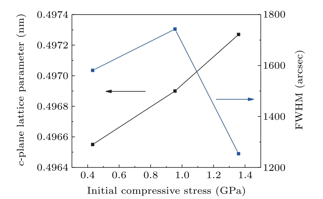
Fig.3.Lattice parameter and FWHM value of XRD(002)rocking curve of the AlN buffer layer dependent on the initial compressive stress.
As was suggested, improving the crystal quality of the AlN buffer layer could increase the compressive stress and reduce the stress relaxation in the subsequently grown GaN film.[9]However,sample B,which has a relatively lower crystal quality than sample A, has a stronger compressive stress than sample A.Therefore,it can be inferred that other factors may also influence the stress states.If we suppose that the GaN was coherently grown on the AlN buffer layer at the initial growth stage of GaN,the stress applied on GaN caused by lattice mismatch can be deduced by Hooke’s law
whereσGaNis the stress applied to GaN film,andEGaNis the Young modulus of GaN and equals 466 GPa.[30]If we assume that in the three samples their stress difference is caused by the lattice mismatch,we can roughly estimate the in-plane lattice difference of the AlN buffer layer since the lattice constants of GaN are basically the same as we mentioned before.According toin-situmonitoring,the stress difference between sample A and sample C is 0.927 GPa and the in-plane lattice difference of the AlN buffer layer should be 0.00063 nm.For an ideal crystal of AlN film under biaxial stress,the difference in the in-plane lattice parameter mentioned above will change thec-plane lattice parameter by 0.00078 nm, which is comparable to the difference obtained by HRXRD (0.00072 nm).Hence,we speculate that the compressive stress applied to the GaN film was probably changed by the difference in the lattice parameter of AlN buffer layer.
Raman spectra were also measured at room temperature by 532 nm laser beam excitation to show the final stress state of GaN films after the cooling process as shown in Fig.4.Since the E2(high) phonon peak is non-polar and sensitive to the biaxial stress,it is usually used to check the stress state in the sample[32]according to the formula shown below:[33]
where Δωis the shift of the E2(high) peak compared to the valueωin the intrinsic condition,whereωis 567.6 cm-1[34]for GaN andKis 4.3 cm-1·GPa-1which represents the stress coefficient[35]for GaN.The residual stresses in the GaN films of samples A,B,and C at room temperature in the GaN film were calculated as 0.68 GPa,0.57 GPa,and 0.49 GPa respectively, and they were all tensile stress.The tensile stresses should be mainly generated during the cooling process and were not fully compensated by the compressive stress induced at the GaN/AlN heterostructure.The decreasing trend of residual tensile stress from sample A to sample C shows the increasing compressive stress applied to GaN during the growth.Herein from the result of Raman spectra the difference of stress between sample A and sample C is 0.19 GPa, which is far less than those estimated from thein-situcurvature monitor.This shows that there might be additional ways to relax the tensile stress from CTE mismatch during or after the cooling process.
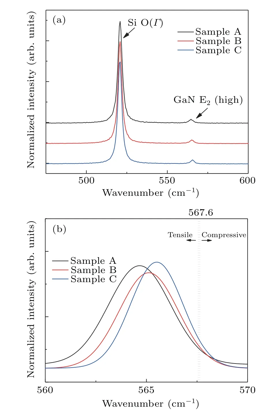
Fig.4.(a)Raman spectra of three GaN film samples which are grown with different AlN buffer layers on Si.(b)Details of the Raman shift of the GaN E2 (high)peak.
In general, there are two ways in which the high strain energy in GaN film is released: one is crack formation and the another is surface roughening.[36-39]Figure 5 shows the GaN surface morphologies measured by the Normaski microscope.There are many cracks found in sample A.With the compressive stress increasing,the number of cracks in the central part of a 2-inch wafer decreases obviously and no crack was found in sample C in the central part of the wafer.It can also be found that the surface of sample C is more flattened with the help of the Normaski microscope.Figure 6 presents the AFM images of GaN films of samples A-C.The root mean square roughnesses(RMS)of the GaN surfaces are 2.78 nm, 0.514 nm, and 0.438 nm respectively and decrease from sample A to sample C.Many pits can be found in sample A and sample B and some protrusions can also be found in sample A.With the compressive stress increasing,no additional pathway such as pits,protrusions or crack formation for strain energy release was needed,as can be seen in Figs.5 and 6.Relief of strain energy by changing the surface morphology reduces the difference in residual stress between these samples and so the gap is apparently smaller (0.19 GPa).Theωscan FWHMs of the rocking curves of the GaN epitaxial layer of samples A-C are measured by HRXRD and the results are presented in Fig.7.Both the FWHM values of the(002)and(102)planes get narrower from sample A to sample C,which indicates that the TDD in sample C is the lowest.It can be proven in Figs.5-7 that a larger compressive stress is beneficial to form a more flattened surface morphology with fewer cracks and have a better crystal quality with a lower TDD in the GaN film.

Fig.5.Normaski microscope images of GaN films deposited on an AlN buffer layer with different lattice parameters: (a)sample A,(b)sample B,(c)sample C.

Fig.6.AFM images(5μm×5μm)of GaN films deposited on an AlN buffer layer with different lattice parameters.

Table 2.Growth conditions of the AlN buffer layer in the orthogonal experiment and the result of lattice parameters measured by HRXRD,where K1, K2, and K3 represent the sum of the lattice parameters for the three levels of each factor and R is the range for each factor.The error in the c-plane lattice parameter is±0.00006 nm.
Finally, we discuss how to better modify the lattice parameter of the AlN buffer layer during growth.A further orthogonal experiment based on samples A to C was done to find which is the key factor that affects the lattice parameter of the AlN buffer layer.The growth conditions and the results of measurement of experiments 1-9 are listed in Table 2,whereKrepresents the sum of the lattice parameter values for the same level of each factor, for example,K1for the TMA preflow time is the sum of lattice parameter values in Exp.1, Exp.2, and Exp.3 and the answer is 1.49055.Ris the range for each factor which is obtained by subtracting the minimum value from the maximum value ofKin the same column.The three variables, i.e., TMA preflow time (20 s,30 s, 60 s), growth rate of the AlN buffer layer (0.056 nm/s,0.067 nm/s, 0.083 nm/s) and growth temperature of the AlN buffer layer(1025°C,1050°C,1075°C)are set to three different levels in the experiments and the other conditions,such as the thickness of the AlN buffer layer, V/III mole ratio and so on,were kept constant.The calculated rangeRof different variables can be considered as the degree of correlation between the experimental result and the variables.It was shown that the influence of the growth rate of the AlN buffer layer on lattice parameter values is almost 3.5 times as large as that of TMA preflow time and 10 times as large as that of growth temperature.It is thought-provoking to further explore why the growth rate of the AlN buffer layer,in addition to the preflow condition and growth temperature which were often optimized during the AlN growth,[16,20-23,25]can have such a large influence in effectively affecting the lattice parameter and controlling the stress state.The relation between the lattice parameter and growth rate is presented in Fig.8.The lattice parameter was acquired by averaging the values in the orthogonal experiment.The largestc-plane lattice parameter(i.e.,the smallest in-plane lattice parameter)was obtained at the middle growth rate and the trend is the same as in samples A,B,and C.The exact mechanism of the relation between growth rate and the lattice parameter is still unknown.Here we speculate a possible mechanism as follows.When the growth rate decreases from 0.067 nm/s to 0.053 nm/s, AlN has more time to relax itself from the Si substrate;therefore,the in-plane lattice gets smaller gradually (the in-plane lattice parameter of (111) Si is larger than AlN) and results in a largerc-plane lattice parameter if we assume the process is realized by biaxial stress.As the growth rate increases from 0.067 nm/s to 0.083 nm/s,more TDs are generated in the AlN buffer layer and this process leads to a decrease in interplanar spacing.This is reflected in sample B which had the largest number of TDs as shown in Fig.3.

Fig.7.FWHM of the GaN peak in XRD(002)and(102)rocking curves and the RMS of the GaN surface roughness dependent on initial compressive stress.

Fig.8.Average c-plane lattice parameter of the AlN buffer layer in the orthogonal experiment at different growth rates.
4.Conclusion
In summary,in the growth of a GaN/AlN/Si heterostructure system,modulating the lattice parameter of the AlN buffer layer properly by changing the growth rate can help to achieve better stress control and increase the compressive stress at the GaN/AlN heterostructure interface.Meanwhile, a smoother surface morphology of GaN with no pits and lower density of threading dislocations can be obtained with a larger compressive stress.The growth rate of the AlN buffer layer should be an important factor that affects the lattice parameter of the AlN buffer layer as confirmed by an analysis based on a series of orthogonal experiments.
Acknowledgments
Project supported by Beijing Municipal Science&Technology Commission, Administrative Commission of Zhongguancun Science Park (Grant Nos.Z211100007921022 and Z211100004821001), the National Natural Science Foundation of China (Grant Nos.62034008, 62074142, 62074140,61974162,61904172,61874175,62127807,and U21B2061),Key Research and Development Program of Jiangsu Province(Grant No.BE2021008-1), Beijing Nova Program (Grant No.202093),Strategic Priority Research Program of Chinese Academy of Sciences(Grant No.XDB43030101),and Youth Innovation Promotion Association of Chinese Academy of Sciences(Grant No.2019115).
猜你喜歡
思維與智慧·上半月(2025年2期)2025-02-21 00:00:00
民間故事選刊(2022年20期)2022-10-30 01:10:29
民間故事選刊·下(2022年10期)2022-05-30 15:51:26
參花(上)(2022年4期)2022-05-23 22:16:48
Chinese Physics B(2021年1期)2021-01-21 02:15:38
應(yīng)用數(shù)學(xué)(2021年1期)2021-01-07 01:23:26
東坡赤壁詩詞(2020年2期)2020-06-04 15:44:10
今日財(cái)富(2017年32期)2017-10-19 20:30:20
小天使·四年級(jí)語數(shù)英綜合(2017年6期)2017-06-07 22:45:22
Journal of Meteorological Research(2014年4期)2014-12-14 06:58:08

- Chinese Physics B的其它文章
- Analysis of cut vertex in the control of complex networks
- Atlas of dynamic spectra of fast radio burst FRB 20201124A
- Investigating the characteristic delay time in the leader-follower behavior in children single-file movement
- Micro-mechanism study of the effect of Cd-free buffer layers ZnXO(X =Mg/Sn)on the performance of flexible Cu2ZnSn(S,Se)4 solar cell
- Thermally enhanced photoluminescence and temperature sensing properties of Sc2W3O12:Eu3+phosphors
- Heterogeneous hydration patterns of G-quadruplex DNA