
Micro-mechanism study of the effect of Cd-free buffer layers ZnXO(X =Mg/Sn)on the performance of flexible Cu2ZnSn(S,Se)4 solar cell
2023-03-13 09:20:30CaixiaZhang張彩霞YalingLi李雅玲BeibeiLin林蓓蓓JianlongTang唐建龍QuanzhenSun孫全震WeihaoXie謝暐昊HuiDeng鄧輝QiaoZheng鄭巧andShuyingCheng程樹英
Chinese Physics B 2023年2期
關(guān)鍵詞:彩霞
Caixia Zhang(張彩霞) Yaling Li(李雅玲) Beibei Lin(林蓓蓓) Jianlong Tang(唐建龍)Quanzhen Sun(孫全震) Weihao Xie(謝暐昊) Hui Deng(鄧輝)Qiao Zheng(鄭巧) and Shuying Cheng(程樹英)
1College of Physics and Information Engineering,and Institute of Micro-Nano Devices and Solar Cells,Fuzhou University,Fuzhou 350108,China
2Jiangsu Collaborative Innovation Center of Photovoltaic Science and Engineering,Changzhou 213164,China
Keywords: ZnMgO/ZnSnO,numerical simulation,Cd-free buffer,heterojunction interface
1.Introduction
Kesterite Cu2ZnSn(S,Se)4(CZTSSe)solar cells have the potential to replace Cu(In, Ga)(S, Se)2(CIGSSe) solar cells owing to their environmentally friendly, earth-abundant, and less-toxic constituent elements.[1]CZTSSe thin-film shows ptype conductivity,high light absorption coefficients of approximately 104cm-1,and direct bandgaps of 1.0 eV-1.5 eV.Currently, the buffer layer in a high-efficiency CZTSSe device is usually CdS with the highest efficiency up to 13%.[2]The CdS layer prepared by the chemical bath deposition (CBD)method can prevent damage to the CZTSSe layer caused by the sputtering deposition method,and Cd2+incorporation into CZTSSe can greatly reduce the surface defects of the CZTSSe layer, improving the device efficiency.However, CdS buffer layers will not be conducive to long-term commercial development due to the toxicity of Cd and the hazardous waste generated during the preparation process.And the CdS layer with a 2.4-eV bandgap can cause optical absorption loss in the short wavelength, influencing the light utilization of the CZTSSe layer and the short-circuit current density(Jsc)of the device.[3]To replace the toxic CdS buffer,several researchers are investigating Cd-free CZTSSe solar cells with high efficiencies, such as In2S3,[4]ZnO,[5]Zn (O, S),[6]Zn1-xMgxO(ZnMgO),[7]and Zn1-xSnxOy(ZnSnO).[8]
When searching for new alternative Cd-free buffer layer materials, the focus should first be on the energy band alignment between the absorber layer and the buffer layer.The conduction band offset(CBO)between the CZTSSe absorber and the buffer layer has profound effects on the transport and collection of carriers.Among those buffers, we choose the ZnMgO or ZnSnO buffer layer with a wide bandgap and tunable bandgaps, which has the advantages of alleviating the short-wavelength optical loss and environmental protection of the elements, especially, the CBO of the heterojunction interface can be controlled by adjusting the element doping ratio.[9,10]ZnMgO and ZnSnO are ternary alloys formed by ZnO with metal oxides MgO and SnO, respectively, which may be important buffer layer candidates in CZTSSe solar cells.Liuet al.[11]investigated the electronic structure characteristics of Zn1-xMgxO alloys with different Mg components, and it is found that the band gaps in Zn1-xMgxO increase with increasing Mg composition, and the conduction band arrangement and Fermi level position are related to the Mg concentration.For Zn1-xSnxOymaterials,Guoet al.confirmed that as the Sn concentration increases, the band gap of the material changes significantly, and the O 2p orbital(valence band) and Zn 3d, 4s, and 4p (conduction band) orbitals are affected simultaneously.[12]According to these reports, ZnMgO and ZnSnO can control the interfacial CBO by regulating the Mg/(Zn+Mg)and Sn/(Zn+Sn)ratios.Several experimental studies have confirmed the feasibility of replacing the traditional CdS layer with the ZnMgO and Zn-SnO layers.Hironiwaet al.fabricated CZTSSe/ZnMgO solar cell on Mo/SLG substrates with an efficiency of 2.76%.[7,13]Kimet al.reported over 11% efficiency for CZTSSe/ Zn-SnO heterojunction cells fabricated by sputtering on Mo/SLG substrates.[8]There are few reports on flexible cadmium-free CZTSSe solar cells using Mo foil substrates.Our group focuses on the study of Mo-foil-based flexible CZTSSe solar cells.Flexible solar cells have attracted wide attention because of their ability to achieve photovoltaic building integration and wearable functions.
For the exploration and research of solar cells, numerical simulation is one of the methods for planning and designing high-performance solar cells.In our work, the SCAPS-1D software is used to simulate the photovoltaic performance of solar cell structure Mo/CZTSSe/ZnMgO or (ZnSnO)/i-ZnO/ITO/Ag.Different concentrations of Mg or Sn doped into ZnO are investigated to form a more favorable energy band matching for optimal solar cell performance.The simulation results show that the Zn1-xMgxO and Zn1-xSnxOylayers achieve the best device efficiencies at doping concentrations (x) 0.1 and 0.2, respectively.However, the efficiency of CZTSSe/Zn0.9Mg0.1O and CZTSSe/Zn0.8Sn0.2O devices is quite different.Based on the simulation results,we also study the effects of the thickness and carrier concentration of the Cd-free buffer layers on the solar cell performance and further analyze the physical mechanism of CBO between the buffer layer and the CZTSSe absorber affecting the carrier transmission.Finally,the solar cell structure is optimized and designed by numerical simulations, flexible CZTSSe/Zn0.9Mg0.1O and CZTSSe/Zn0.8Sn0.2O heterojunction solar cells are experimentally fabricated with the optimal doping ratio, and the related tests and characterizations are performed.The doping of Mg reduces the carrier concentration and mobility of the ZnMgO buffer layer and increases the resistivity, which,as demonstrated by numerical simulations, are experimentally confirmed.As a result, the electrical conductivity of the ZnMgO layer needs to be further adjusted.Some literature reported[9,14]that ZnMgO is doped with group III elements such as Al, Ga, or In to achieve high electrical conductivity.In this study,the use of a sputtering ZnSnO layer as promising buffer layer for CZTSSe-based solar cells is demonstrated.This work provides theoretical guidance for the design and fabrication of energy-efficient CZTSSe/ZnMgO and CZTSSe/ZnSnO heterojunction solar cells.
2.Theoretical model and experimental details
2.1.Numerical simulation and device structure
In this paper, the one-dimensional(1D)numerical simulation package solar cell capacitance simulator (SCAPS-1D)is mainly used to explore the effect of carrier properties and interfacial energy band alignment on CZTSSe/buffer heterojunction, which is crucial to solar cell performance.SCAPS-1D is developed by Ghent University in Belgium and is widely used to simulate solar cell devices.[15-17]SCAPS-1D is one of the numerical methods used to simulate solar cells by varying electronic parameters, cell structure,etc.to predict the effect of parameter changes on solar cell performance.The software analyzes the electrical parameters of thin film solar cells by solving Poisson’s equation, the electron continuity equation,and the hole-continuity equation at a steady state.[18]These equations are considered to be some of the fundamental semiconductor equations.Poisson’s equation is expressed as
In this equation,φis electric potential,qis the electronic charge,ε0equals vacuum permittivity,εrstand for relative permittivity,nandpare electron and hole densities,NDandNArepresent the density of ionized donors and acceptors,ρnandρpstand for electron and hole distributions.Continuity equations for electron and hole are expressed as follows:
The parametersJnandJpare electron and hole current densities,Gis generation rate,andRstands for recombination rate.The drift and diffusion equations for electrons and holes are represented by
In these equations,Eis an electric field,μstands for mobility,andDis diffusivity.Equations(4)and(5)are used to describe the carrier recombination mechanisms, electric field distribution,carrier transport mechanism,etc.
After solving Eqs.(1)-(5) above, it is possible to obtain the main parameters of the solar cell,such as open circuit voltage (Voc), short circuit current (Jsc), fill factor (FF), and the power conversion efficiency(PCE).It is also possible to simulate four different measurements:I-V,C-V,C-F,andEQE.
Figure 1 visualizes the solar cell structure of the Mo/CZTSSe/buffer layer(ZnMgO,ZnSnO)/ZnO/ITO/Ag and its band diagram as reported in the article.[19]All materials in this study are set to the uniform band gap.The work function is set to 4.5 and 5.0 for the front contact point (Ag) and the back contact point (Mo), respectively.[20,21]The relevant parameters used to perform our computations are listed in Table 1,and most input parameters for the simulations are mainly collected from relevant theories, literature, or estimated in a reasonable range,etc.[22]This numerical simulation uses the solar illumination spectrum AM 1.5 and the working temperature is set to 300 K.All numerical simulation for this work uses a surface recombination velocity of 107cm/s.We have taken ZnMgO and ZnSnO materials as alternative buffer layers and investigated the effect of the buffer layer band gap,thickness,and carrier concentration on the performance of solar cells.
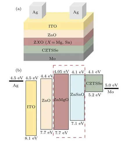
Fig.1.(a) The structure of CZTSSe-based thin-film solar cell with a ZnO-based buffer layer.(b) Diagram band structure of CZTSSe/ZnObased heterojunction.
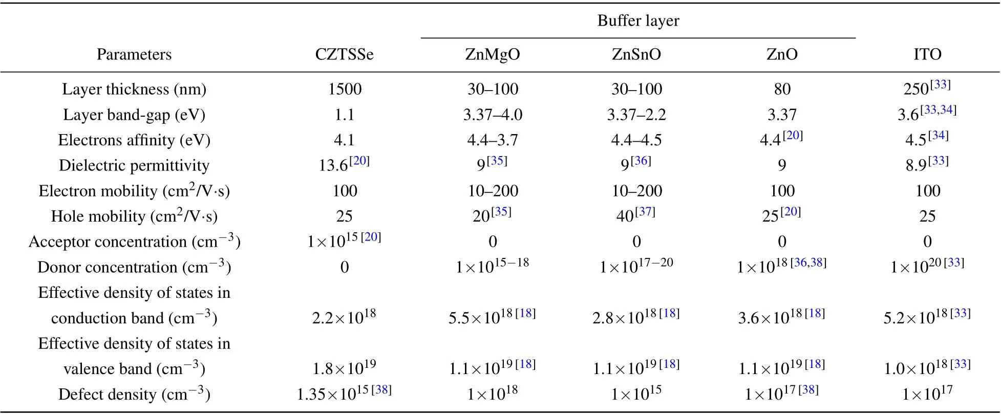
Table 1.Simulation parameters for the models of CZTSSe/ZnMgO and CZTSSe/ZnSnO solar cells.
2.2.Experimental details
2.2.1.Flexible device fabrication
Flexible solar cells with the structure Mo foil/CZTSSe/ZnMgO/ITO or Mo foil/CZTSSe/ZnSnO/ITO(as shown in Fig.S1) are fabricated.The monomers Cu, Zn,Sn, S, and Se were added to a mixture of ethylenediamine(C2H8N2)and 1,2-ethylenedithiol(C2H6S2)in a certain proportion.The precursor solution of CZTSSe was heated and stirred in a heating set at 68°C and 700 r·min-1for 90 min until it was completely dissolved, the stabilizer solution was added, and the heating was continued for 30 min to form a homogeneous and clarified CZTSSe precursor solution.The prepared precursor solution is repeatedly spin-coated onto a flexible Mo foil substrate and pre-annealed to form a CZTSSe prefabricated layer.Then, the treated samples are selenised by rapid thermal processing.A protective gas is continuously passed throughout the selenisation process to produce CZTSSe films.The ZnMgO and ZnSnO buffer layers are prepared by magnetron sputtering.The ITO film(260 nm)is prepared by radio frequency (RF) magnetron sputtering with a sputtering power of 40 W.Finally, the Ag collection grid(~600 nm) is deposited by the thermal evaporation method.The active area for solar cells is 0.21 cm2.
2.2.2.ZnMgO and ZnSnO film deposition
ZnMgO or ZnSnO layers are deposited on CZTSSe absorbers as buffer layers.In the sputtering system, the back pressure (BP) is below 1×10⁻³Pa, while the working pressure (WP) is kept constant at 2 Pa.The ZnMgO films are prepared using a 2-inch (1 inch=2.54 cm) (ZnO:MgO=90:10 at.%) target (99.99%) sputtered in an atmosphere of argon,and ion beam power of 50 W.The ZnSnO layers are prepared using 2-inch Sn(99.99%)and ZnO(99.99%)targets.The sputtering power of Sn and ZnO is 5 W and 50 W,respectively.The thickness of buffer layer is controlled to be about 100 nm by adjusting the deposition time (as shown in Fig.S2).The films deposited with buffer layer are annealed at 200°C under air atmosphere.The schematic diagram of the method for preparing ZnMgO and ZnSnO film are shown in Fig.S3.
2.2.3.Characterizations
The scanning electron microscope(SEM)images are carried out using an Nova Nano SEM 450 with an energy dispersive x-ray(EDX)analyzer.The current density-voltage(J-V)curve is measured using a Keithley 2400 source meter under AM 1.5-G spectrum (100 mW/cm2).The EQE is recorded on a QTest Starion500AD system ranging from 300 nm to 1350 nm.TheC-Vcharacteristics (keithley4200) are measured by using 50 mV and 100-kHz AC excitation source with a DC bias from-1.0 V to 0.4 V.The electrochemical impedance spectroscopy(EIS)spectra are measured by an electrochemical workstation(Bio-Logic SAS,VPS)at the frequency ranging from 1 Hz to 1 MHz.A system consisting of 530-nm monochromatic light,a function generator,and an oscilloscope is used to measure transient photovoltage(TPV)and transient photocurrent(TPC).
3.Results and discussion
3.1.Effect of the buffer layers band gap on CZTSSe solar cell performance
ZnMgO and ZnSnO have attracted attention because of their potential to control the CBO by varying the Mg/(Zn+Mg)and Sn/(Zn+Sn).[23]In this modeling study,we have investigated the effect of different doping concentrations of ZnMgO and ZnSnO on the performance of CZTSSe solar cells.ZnO doping with Mg or Sn elements can change the position of the conductive bands and valence bands,resulting in favorable conduction band offsets(CBO)at the heterojunction interface.The appropriate alignment of the p-type CZTSSe conduction band edge with the n-type buffer layer is one of the main strategies to enhance device performance.
Figure 2 shows the trend ofVoc,Jsc,FF, andPCEof CZTSSe/ZnMgO heterojunction solar cells as the Mg doping concentration varies from 0 to 0.175.For the Zn1-xMgxO buffer layer, the bandgap can be expressed as a function ofxby the following equation:[18]
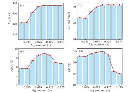
Fig.2.(a)-(d)Influence of the Mg concentration on the performance of CZTSSe/Zn1-xMgxO heterojunction.
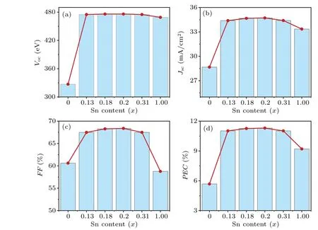
Fig.3.(a)-(d)Influence of the Sn concentration on the performance of CZTSSe/Zn1-xSnxO heterojunction.
When the doping concentration of the ZnMgO buffer layer is in the range from 0 to 0.175, the band gap varies from 3.37 eV to 4.0 eV.These simulations show that the best performance of the CZTSSe/Zn1-xMgxO heterojunction can be achieved when the Mg doping concentration is 0.1, theVoc,Jsc, andFFare 461 mV, 30.25 mA/cm2, and 64.09%,respectively, and the conversion efficiency reaches the maximum 8.93%.For the CZTSSe/ZnSnO heterojunction structure, the Sn doping concentrations are chosen to be 0, 0.13,0.18,0.2,0.31,and 1.0 according to the ZnSnO experimental data reported by Saadatet al.[24,25]The device performance of the CZTSSe/ZnSnO heterojunction reaches a maximum atx=0.2.The results are shown in Fig.3.The best solar cell performance is obtained when the Sn doping concentration reaches 0.2,with an efficiency of 11.3%(Vocof 476 mV,Jscof 34.72 mA/cm2,andFFof 68.38%).
From the numerical simulation results,the improved efficiency of the CZTSSe/ZnMgO and CZTSSe/ZnSnO devices is mainly attributed to the improvedVocandJsc.While the improvement inVocandJsccan be attributed to the suppression of recombination at the CZTSSe/ZnMgO and CZTSSe/ZnSnO heterojunction interface by the appropriate energy band alignment.Furthermore, It is observed that theJscof Zn0.8Sn0.2O (34.72 mA/cm2) is superior to that of Zn0.9Mg0.1O (30.25 mA/cm2) because the reduction of Zn0.8Sn0.2O interfacial recombination can significantly improve theEQE, especially in the short wavelength ranging from 400 nm to 1000 nm (see Fig.S3).This phenomenon is also confirmed in the experimental section.As can be observed in Figs.2 and 3, when the doping concentration of ZnMgO and ZnSnO increases, the efficiency of CZTSSe solar cells increases first and then decreases.This indicates that the CZTSSe/ZnMgO and CZTSSe/ZnSnO heterojunction devices can achieve optimum performance by varying the Mg/(Zn+Mg) and Sn/(Zn+Sn) ratios.Next, we will explain the changing trend of CZTSSe solar cell performance with the band gap of ZnMgO and ZnSnO from the perspective of energy band alignment.
To understand the effect of the conduction band offsets(CBO)on solar cell performance,in the SCAPS-1D software,we choose the “electron affinity rule” (Schottky limit) to directly reflect energy band alignment.[26]The“electron affinity rule”is a way of aligning the bulk model of a semiconductor according to the distanceχ(affinity energy)between the conduction band and the vacuum level of the semiconductor.The model does not take into account Fermi level pinning(which tends to decrease the CBO)and chemical interdiffusion(which tends to increase the CBO).[26]Equation(7)is a calculation of the“ideal”interfacial energy band bias without consideration of Fermi level pinning and interfacial polarization
whereχaandχbare the electron affinity of absorber and buffer layer,φCNL,aandφCNL,bare the charge neutrality level of absorber and buffer layer,The dimensionless screening parameterSis a bulk property of the wider bandgap semiconductor.In Eq.(7)S=1 for the electron affinity rule,it can be simplified to the following equation:
To further analyze the intrinsic causes and mechanisms of the effect of CBO on the performance of CZTSSe devices,we plot the interface band diagrams of(a)CZTSSe/ZnO(x=0),(b)CZTSSe/Zn0.9Mg0.1O,and(c)CZTSSe/Zn0.825Mg0.175O heterojunction, as shown in Fig.4.As the doping concentration of Mg is increased from 0 to 0.1, the energy band alignment at the CZTSSe/buffer heterojunction interface changes from the“cliff”-type to the more favorable“spike”-type.However,when Mg element content further increases up to 0.175,there is a large spike at the heterojunction interface,as shown in Fig.4(c), which is like an electron barrier to impede the carrier transport.Figure 5 shows the different types of energy band alignment formed by the CZTSSe absorption layer with ZnO (x=0), ZnSnO (x=0.2), and SnO buffer layers at the interface,respectively.When the Sn doping concentration (x) increases from 0 to 0.2, the energy band alignment changes from a “cliff” type to a flat “spike” type band interface.The“spike”type band is more conducive to carrier transport than the “cliff”-like energy band alignment.Figure 5(c)shows the formation of an oversized “cliff” type CBO at the CZTSSe/SnO interface, which reduces the cell performance from 11.3%to 9.3%.
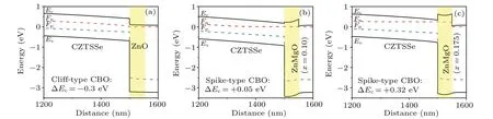
Fig.4.Band diagrams of CZTSSe with(a)ZnO(x=0);(b)ZnMgO(x=0.10);(c)ZnMgO(x=0.175).
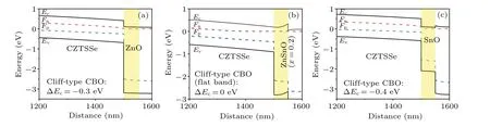
Fig.5.Band diagrams of CZTSSe with(a)ZnO(x=0);(b)ZnSnO(x=0.20);(c)SnO buffer layer.
Band alignment at CZTSSe/buffer interface has a profound effect on the performance of solar cells.The conduction band offset at the heterojunction interface can be divided into two types: cliff-like and spike-like band alignments.From the analysis of Figs.4 and 5, we can note that the CZTSSe/buffer (ZnO or SnO) shows the “cliff”-like energy level alignment because the conduction band minimum of the CZTSSe absorber is more than that of the buffer layer.Therefore, the activation energy of interface recombination(EA) is lower than the band gap of CZTSSe and leads to the interface recombination dominant path.[23]The occurrence of interface recombination results in poor overall device performance as shown in Fig.2 (x=0) and Fig.3 (x=0, 1).As CZTSSe solar cells feature numerous defect states at the interface, particularly deep defect states.After charge separation under forwarding bias, electrons and holes build up and cause severe charge recombination through deep energy level defects at the heterojunction interface with a cliff-like type.The better band alignment in Fig.4(b)CZTSSe/Zn0.9Mg0.1O and Fig.5(b) CZTSSe/Zn0.8Sn0.2O interface shows a small spike-like CBO (+0.05 eV) or an almost “flat” spike band favorable to minority carrier transport and collection.This is why Fig.2 Zn1-xMgxO (x=0.1) and Fig.3 Zn1-xSnxO(x=0.2) achieve the best device efficiency.When the spike structure is formed at the interface,the interface level structure can further create a slight barrier to prevent interface recombination.However,when the spiky conduction band offset exceeds a suitable range(0 eV-0.3 eV),it will create a substantial obstacle to blocking electron transport.The results confirm that the band conduction offset of CZTSSe/Zn1-xMgxO and CZTSSe/Zn1-xSnxO can be controlled by varying the Mg/(Zn+Mg)and Sn/(Zn+Sn).Energy band alignment at the heterojunction interface is a key factor when selecting materials to replace toxic CdS buffer layers.
On the other hand,it is observed from Figs.4 and 5 that the difference in device performance between the Zn1-xMgxO and Zn1-xSnxO as buffer layers is great, although the doping concentration of the two is at the optimal valuesx=0.1 and 0.2, respectively.This suggests that in addition to focusing on the energy band alignment of the interface, other factors should also be considered when selecting a suitable cadmiumfree buffer layer.The following simulation will investigate the effect of carrier concentration and thickness of Zn0.9Mg0.1O and Zn0.8Sn0.2O layers on device performance.
3.2.Effect of buffer layer carrier concentration and thickness on CZTSSe solar cell performance
The heterojunction interface formed by the buffer and the absorber layers plays a crucial role in the collection and transport of photogenerated charge carriers,so the buffer layer carrier concentration and thickness that affect the interface performance are important parameters.The carrier concentration and thickness of the Zn0.9Mg0.1O buffer layer vary between 1015cm-3and 1018cm-3and 30 nm-150 nm respectively,then,so the efficiency of the CZTSSe/Zn0.9Mg0.1O solar cells varies from 3.04% to 11.18%, as shown in Fig.6.It is observed from Fig.6 thatJsc,FF,andPCEare almost independent of the buffer thickness when the carrier concentration is more than 1017cm-3.However, when the concentration of Zn0.9Mg.1O carrier is less than 1016cm-3, the performance of the device decreases with the increasing thickness of the Zn0.9Mg0.1O buffer layer rises.
Therefore, choosing a proper buffer layer thickness can improve the deterioration of cell performance.When the carrier concentration is less than 1016cm-3,the resistivity of the Zn0.9Mg0.1O layer increases, thus the thicker thickness will further reduce the performance of the device.
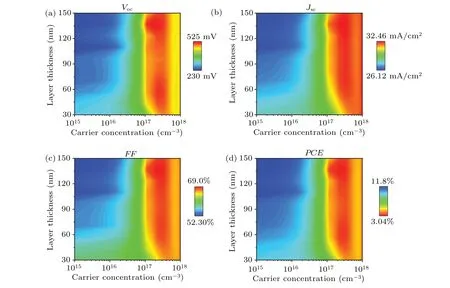
Fig.6.Contour plot of the effect of the thickness and carrier concentration of the ZnMgO buffer layer on the performance parameters of CZTSSe solar cells.
Figure 7 investigates the effect of the carrier concentration and thickness of the Zn0.8Sn0.2O layer on device performance.The carrier concentration and thickness of the ZnSnO buffer layer vary from 1017cm-3to 1020cm-3and 30 nm to 150 nm,respectively.It is observed that the solar cell performance deteriorate seriously when the carrier concentration is less than 1018cm-3and the layer thickness is less than 50 nm.And when the Zn0.8Sn0.2O layer is thinner than 45 nm with the carrier concentration is 1017cm-3,the performance of the device is only 10.49%.However,when the carrier concentration is more than 1019cm-3and the thickness is less than 60 nm,the highest device efficiency is up to 11.31%.The performance of the CZTSSe/Zn0.9Mg0.1O solar cells in Fig.6 varies very significantly with the carrier concentration and thickness of the Zn0.9Mg0.1O buffer layer(PCEfrom 3.04%to 11.18%),which is due to the low Zn0.9Mg0.1O carrier concentration and the corresponding rapidly increasing resistivity, resulting in poor device performance.Therefore, the performance of the device composed of a buffer layer with low carrier concentration is more susceptible to the buffer layer thickness.Besides, the height of the interface barrier between the absorber layer and the buffer layer is affected by the buffer carrier concentration.[27]When the carrier concentration is low,the electron Fermi level is far away from the conduction band,and the interface barrier height increases significantly.For the Zn0.8Sn0.2O buffer layer, the relatively high carrier concentration saturates the device performance,thus the buffer layer thickness has relatively little effect on the performance.
As can be seen from Figs.6 and 7, the optimum device performance can be obtained for the Zn0.9Mg0.1O and the Zn0.8Sn0.2O buffer layer with a higher carrier concentration.For ZnMgO, Mg doping (Mg content fromx=0.1 to 0.3) reduces the carrier concentration and mobility, resulting in a low conductivity of ZnMgO.This result is confirmed in the study of ZnMgO by Ginleyet al.[9]However, according to Deepak, the carrier concentration of ZnO:Sn films deposited under a high vacuum can reach the order of 1019cm-3or even higher.[28]This is why we chose 1017cm-3and 1019cm-3as the carrier concentrations for Zn0.9Mg0.1O and Zn0.8Sn0.2O, respectively.When the carrier concentration of Zn0.9Mg0.1O is 1017cm-3, the effect of thickness on device performance is not significant.While at a carrier concentration of 1019cm-3for Zn0.8Sn0.2O, it can be seen that a thinner thickness gives better device performance.However,the buffer layer is hardly controlled experimentally when the thickness is less than 50 nm.To ensure that the thickness of the buffer layer does not cause a loss of light absorption,and that its thickness is strong enough to diffuse the photogenerated carriers outside the depletion zone,this requires determining a suitable threshold thickness.[18]
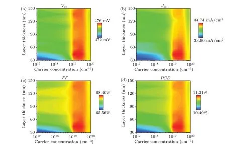
Fig.7.Contour plot of the effect of the thickness of the ZnSnO buffer layer and carrier concentration on the performance parameters of CZTSSe solar cells.
3.3.Effect of buffer layer thickness on CZTSSe solar cell performance
The thickness and carrier concentration of the buffer layer are the key parameters to be considered when selecting an alternative buffer layer material.They influence the transport and collection of the photogenerated carrier.To further optimize the buffer layer thickness, we investigate the effect of the cadmium-free buffer layer thickness on the device performance, as shown in Fig.8, where the thickness of the buffer layers Zn0.9Mg0.1O and Zn0.2Sn0.8O is increased from 30 nm to 150 nm.
For the Zn0.9Mg0.1O layer,the device performance is significantly improved when the thickness increases from 30 nm to 80 nm,the open circuit voltage(Voc)increases sharply from 402 mV to 467 mV and the short circuit current(Jsc)increases from 29.25 mA/cm2to 30.95 mA/cm2, both of which reach saturation at a thickness of 80 nm.For the Zn0.9Mg0.1O layers with low carrier concentration, the thinner thickness cannot provide the width of the depletion region required for carrier transport, resulting in carrier recombination at the interface.Moreover, the Zn0.9Mg0.1O layer with low carrier concentration has low resistivity that hinders the transport of the carriers, which have been recombined even before reaching the Ag electrode, so that the device performance decreases when the buffer layer thickness is greater than 120 nm, especially theFF.We chose 80 nm as the optimum thickness for the Zn0.9Mg0.1O buffer layer.For the Zn0.2Sn0.8O,Voc,Jsc, andPCEshow a similar trend, with a slight reduction at a thickness greater than 80 nm,while theFFincreased slightly after 80 nm.This means that the Zn0.2Sn0.8O layer with high carrier concentration has high conductivity, and the carrier transport and collection are less affected by the thickness.But it causes some light absorption loss when the buffer layer thickness is greater than 80 nm.Based on the above studies of the carrier concentration and thickness,we chose 80 nm as the thickness of the Zn0.2Sn0.8O buffer layer.
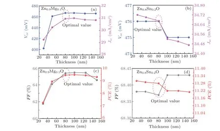
Fig.8.Open circuit voltage(Voc)and short circuit current(Jsc)as a function of(a)Zn0.9Mg0.1O and(b)Zn0.8Sn0.2O thicknesses; fill factor(FF)and efficiency(PCE)as a function of(c)Zn0.9Mg0.1O and(d)Zn0.8Sn0.2O thicknesses.
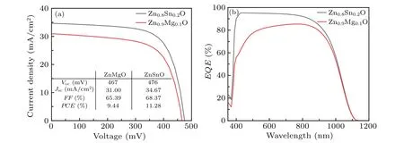
Fig.9.(a) Current density-voltage curves and (b) EQE curve of the CZTSSe solar cells with different buffer layers Zn0.9Mg0.1O and Zn0.8Sn0.2O obtained by SCAPS simulation.
Based on the optimal stimulation parameters,figures 9(a)and 9(b) show the comparison of theJ-Vcharacteristics and the EQE responses between the CZTSSe/Zn0.9Mg0.1O and CZTSSe/Zn0.2Sn0.8O devices,respectively.From the SCAPS simulation results, for the CZTSSe/Zn0.9Mg0.1O solar cell,thePCEof the solar cell with a thickness of 80 nm (optimal value) is 9.44% with a carrier concentration of 1017cm-3in the Zn0.9Mg0.1O buffer layer.For the CZTSSe/ Zn0.8Sn0.2O solar cell, thePCEof the solar cell with a thickness of 80-nm optimal value) is 11.28% with a carrier concentration of 1019cm-3in the Zn0.8Sn0.2O buffer layer.The ZnMgO band gap is higher than the ZnSnO layer, but the spectral response becomes worse at short wavelengths(Fig.9(b)),which may be due to the reduced carrier collection.In this study,we discover that thickness has less impact on the buffer layers with high carrier concentration(ZnSnO),and the buffer layers with low carrier concentration(ZnMgO)had significantly worse performance (VocandJsc) due to deterioration of carrier transport properties.The simulation results show that the ZnSnO buffer layer is more suitable as an alternative buffer layer, while the ZnMgO material has limitations due to its material properties.
3.4.Experimentally fabricated CZTSSe/ZnMgO (or Zn-SnO)heterojunction solar cells
Figures 10(a)-10(b) showJ-Vcurves and EQE spectra of CZTSSe/Zn0.8Sn0.2O and CZTSSe/Zn0.9Mg0.1O solar cells.The ratios of Mg/(Zn+Mg) and Sn/(Zn+Sn) prepared by sputtering are 0.1 and 0.2, respectively, as measured by EDX(see Fig.S4).Table 2 lists the performances of the solar cell (Voc,Jsc,FF, andPCE).The best CZTSSe/Zn0.8Sn0.2O devices achieve an efficiency of 7.58%, which is larger than that of the best CZTSSe/Zn0.9Mg0.1O devices(3.26%),mainly in theJscandFF.Hironiwaet al.reported CZTSSe/ZnMgO device efficiency of 2.75%on a rigid substrate,with the lowJsc(12 mA/cm2)being the key factor limiting its performance improvement.Since the conductivity of the Mg-doped ZnO layer is adversely reduced,the mobility is also significantly reduced,and the device performance is reflected in the smallerFFand the lowerJsc.The CZTSSe/Zn0.8Sn0.2O devices yield a higherJscthan the CZTSSe/Zn0.9Mg0.1O device,which is mainly due to higher absorption in the short wavelength range as can be seen in the external quantum efficiency (EQE) curves shown in Fig.10(b).
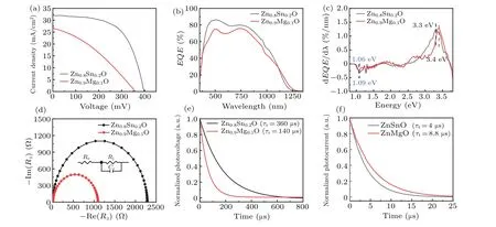
Fig.10.(a) The J-V curves under standard AM 1.5 illumination; (b) external quantum efficiency (EQE); (c) d(EQE)/d(λ) curves for CZTSSe/Zn0.8Sn0.2O and CZTSSe/Zn0.9Mg0.1O devices.(d) Nyquist plot of devices with the equivalent electrical circuit model.(e) TPV decay and(f)TPC decay of typical devices.
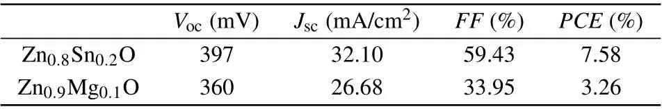
Table 2.The device parameters derived from J-V curves.
The ZnMgO and ZnSnO buffer layers effectively improve the optical absorption loss caused by the traditional CdS layer in the short wavelength band.The band gaps of different layers in the device can be obtained byEQEcurves calculation.The band gaps of the absorber layer in the CZTSSe/Zn0.8Sn0.2O and CZTSSe/Zn0.9Mg0.1O devices are 1.09 eV and 1.06 eV, respectively, and the smaller band gap of CZTSSe/ Zn0.9Mg0.1O device may be due to the diffusion of Mg into the absorber layer.The narrowing of the band gap of the absorber layer leads to a smallerVocof CZTSSe/Zn0.9Mg0.1O devices (360 mV) than CZTSSe/Zn0.8Sn0.2O (397 mV) devices.[29]We calculate the diode parameters of the device through theJ-Vcurve,and the specific formula is as follows:[30]
whereAis the ideality factor,Rsis series resistance,andGshis shunt conductance,JLandJ0are the photocurrent and reverse saturation current density,respectively.
The conductivity of the Zn0.9Mg0.1O layer decreases due to the doping of Mg, makingRs(6.87 Ω/cm2) andGsh(24.92 mS/cm2) increase, while the Zn0.8Sn0.2O layer has a relatively high carrier concentration and high conductivity,reducingRs(0.33 Ω/cm2)andGsh(6.39 mS/cm2).Jscis mainly affected byRsandGsh, so theJscof the Zn0.9Mg0.1O device is smaller than that of the Zn0.8Sn0.2O device in both theoretical simulations and experiments.As shown in Table 3,Gsh,A,andJare associated with the recombination in the depletion zone of the heterojunction interface, indicating that the heterojunction quality formed by Zn0.9Mg0.1O is worse than that formed by Zn0.8Sn0.2O.By using the SCAPS-1D simulation,we find that the carrier concentration has a significant effect on the device performance.
To investigate the carrier transport and recombination properties of CZTSSe/Zn0.8Sn0.2O and CZTSSe/Zn0.9Mg0.1O heterojunction devices,EIS,TPC,and TPV measurements are performed.The EIS impedance diagram is obtained by fitting the simple equivalent circuit model in Fig.10(d).The equivalent circuit model consists of a resistorRsin series,a resistorRjand capacitorCein parallel.The diameter of the semicircle in the impedance diagram is equal to the value of the recombination resistanceRj.[31]From the EIS spectra(Fig.10(d)),it is clear that CZTSSe/Zn0.8Sn0.2O device shows higherRjvalues compared to the CZTSSe/Zn0.9Mg0.1O device, which means that the interface recombination of CZTSSe/Zn0.8Sn0.2O heterojunction device is less.This is further proven by the TPV and TPC measurements of the heterojunction quality.A charge recombination lifetime value (τr) can be obtained from TPV measurements in Fig.10(e), which is used to characterize the charge recombination and defect density in the solar cell.The CZTSSe/Zn0.9Mg0.1O device shows a smaller charge recombination lifetime (τr= 140 μs) than CZTSSe/Zn0.8Sn0.2O device (τr=360 μs), which also confirms that the CZTSSe/Zn0.9Mg0.1O heterojunction has a large defect density and severe interfacial recombination, resulting in a lowJscandFF.The charge transfer lifetimes (τt) of the CZTSSe/Zn0.8Sn0.2O devices and CZTSSe/Zn0.9Mg0.1O devices measured at the condition of the short circuit are shown in Fig.10(f).Theτtcharacterizes the ability of the device to extract and transfer charges.It can be seen that the CZTSSe/Zn0.8Sn0.2O devices(4μs)decay faster than the CZTSSe/Zn0.9Mg0.1O devices(8.8μs).This indicates that the charge extraction and transport of the CZTSSe/Zn0.8Sn0.2O device are better than that of the CZTSSe/Zn0.9Mg0.1O device, which is one of the reasons for the higherJscof CZTSSe/Zn0.8Sn0.2O device.From the TPC,TPV,and EIS,it is shown that the CZTSSe/Zn0.9Mg0.1O device has severe interfacial charge recombination and poor charge extraction and transport,which is in agreement with the previous theoretical simulations.
In order to further investigate the band bending of CZTSSe/Zn0.9Mg0.1O and CZTSSe/Zn0.8Sn0.2O devices,capacitance-voltage(C-V)measurements are performed(see Fig.S5).[32]The carrier concentration in the absorber layer(Nc-v),depletion width(Wd),and built-in voltage(Vbi)can be calculated from theC-Vcurve, as shown in Table 3.After the photogenerated electron-hole pairs reach the depletion region, they are collected by electrodes under the separation of the built-in electric field.It can be seen that the wider the width of the depletion region, the more the separated electron-hole pairs, and the larger the photocurrent that is generated.TheVbiandWdof the CZTSSe/Zn0.8Sn0.2O device (0.410 V and 0.181 μm) are higher than that of the CZTSSe/Zn0.9Mg0.1O device (0.233 V and 0.104 μm).This is consistent with the higherVoc,FF, andJscobtained by the CZTSSe/Zn0.8Sn0.2O device in numerical simulations of the experimental results,indicating that Zn0.8Sn0.2O material may be a promising and inexpensive buffer layer alternative to CdS.

Table 3.The device parameters derived from J-V curves and C-V curves.
4.Conclusions
In conclusion, we used numerical modeling and experimental results to examine the potential of the widebandgap non-toxic materials ZnMgO and ZnSnO as alternative buffer layers.To investigate the impacts of interfacial CBO, carrier concentration, and thickness on device performance, SCAPS modeling of ZnO-based buffer layer devices is carried out.The simulation results show that the best device performance is obtained for CZTSSe/Zn0.9Mg0.1O and CZTSSe/Zn0.8Sn0.2O devices.This is due to the small“spikelike” CBO (+0.05 eV) or almost “flat band” formed at the heterojunction interface of these two devices that facilitate the transport and collection of minority carriers.It is observed that the Zn0.8Sn0.2O devices with high carrier concentration obtain more than 11%PCEwith a small effect of thickness on device performance.The Zn0.9Mg0.1O devices display inferiorPCE.For Zn0.9Mg0.1O material, Mg doping causes a decrease in carrier concentration and an increase in resistivity.It further leads to inefficient carrier transport and increased interfacial recombination.Our experimental results show that the devicePCEvalues of the Zn0.9Mg0.1O and Zn0.8Sn0.2O thin films prepared by sputtering as buffer layers are 3.26% (the most efficient flexible CZTSSe/ZnMgO solar cells currently available)and 7.58%,respectively.The simulation results indicate that the Zn0.9Mg0.1O material has largeGshandRs, resulting in reducedJscandFF.It is further supported by our experimental data.The poor quality of the CZTSSe/Zn0.9Mg0.1O PN junction can also be confirmed byC-V, EIS, TPV, and TPC.Through both numerical simulations and experimental tests,it is proved that the ZnSnO buffer layer has the potential to replace the toxic CdS layer.The process of preparing ZnSnO by the sputtering method is more suitable for large-scale commercial development.We believe that further optimization of the cadmium-free buffer layer production process can greatly improve the efficiency of environmentally friendly kesterite solar cells.
Acknowledgements
Project supported by the National Natural Science Foundation of China (Grant Nos.62074037 and 52002073) and the Fund from the Fujian Science & Technology Innovation Laboratory for Optoelectronic Information of China (Grant No.2021ZZ124).The authors also thank Testing Center of Fuzhou University for facility access.
猜你喜歡
藝術(shù)大觀(2023年14期)2023-07-06 11:48:05
做人與處世(2022年4期)2022-05-26 21:50:38
應(yīng)用數(shù)學(xué)(2019年3期)2019-06-27 09:58:16
文藝生活·中旬刊(2018年12期)2018-05-29 07:58:16
小學(xué)生作文選刊(2017年2期)2017-12-05 01:19:18
絲路藝術(shù)(2017年5期)2017-04-17 03:11:51
Transactions of Nanjing University of Aeronautics and Astronautics(2015年2期)2015-11-24 02:39:15
少年文藝·開心閱讀作文(2015年9期)2015-09-28 07:43:47
學(xué)周刊·下旬刊(2014年12期)2015-06-02 23:38:32
學(xué)周刊·下旬刊(2014年9期)2014-10-20 02:57:07

- Chinese Physics B的其它文章
- Analysis of cut vertex in the control of complex networks
- Atlas of dynamic spectra of fast radio burst FRB 20201124A
- Investigating the characteristic delay time in the leader-follower behavior in children single-file movement
- Thermally enhanced photoluminescence and temperature sensing properties of Sc2W3O12:Eu3+phosphors
- Heterogeneous hydration patterns of G-quadruplex DNA
- Analysis of refraction and scattering image artefacts in x-ray analyzer-based imaging