
High-sensitive phototransistor based on vertical HfSe2/MoS2 heterostructure with broad-spectral response
2022-12-28 09:55:28WenDeng鄧文LiShengWang汪禮勝JiaNingLiu劉嘉寧TaoXiang相韜andFengXiangChen陳鳳翔
Chinese Physics B 2022年12期
關(guān)鍵詞:鳳翔
Wen Deng(鄧文), Li-Sheng Wang(汪禮勝), Jia-Ning Liu(劉嘉寧),Tao Xiang(相韜), and Feng-Xiang Chen(陳鳳翔)
Department of Physics Science and Technology,School of Science,Wuhan University of Technology,Wuhan 430070,China
Keywords: HfSe2/MoS2 heterostructure,phototransistor,high-sensitive,broad-spectral response
1. Introduction
In recent years,the two-dimensional(2D)transition metal dichalcogenides(TMDs)have attracted extensive attention in optoelectronic devices due to their unique structures and excellent photoelectric properties.[1–4]Among TMDs,the MoS2has been extensively employed in phototransistors,and many researches have shown that the MoS2phototransistors have good photodetection performance in the visible region.[3,5]However,the high dark current,slow photoresponse and high power of the MoS2phototransistors limit their further development. So, in order to improve these problems, researchers have made a lot of efforts, such as inserting a perovskite absorption layer,[6]Au nanoparticles or nanoarrays to enhance light absorption,[7–9]decorating different quantum dots (e.g., PbS,[10]MoS2,[11,12]HgTe,[13]) to gain high photoelectric detectivity,and constructing homojunctions and different types of heterostructures (e.g., WSe2/WSe2,[14]PtS2/WSe2,[15]WSe2/Bi2Se3,[16]Cu9S5/PtS2/WSe2,[17]) to improve photoresponse and achieve ultralow power or selfdriven detection,etc.[18–21]
Among the methods of boosting the properties of photodetector, fabricating the van der Waals (vdW) heterostructures based on the vertical stacking of two 2D materials is a convenient and feasible approach, which can combine the advantages of the two materials, and produce some unusual properties and phenomena.[22]A series of MoS2-based vertical vdW heterostructure photodetectors,such as SnSe2/MoS2,[19]MoTe2/MoS2,[23]MoO3/MoS2,[24]GaSe/MoS2,[25]and PdSe2/MoS2,[20]have exhibited excellent photodetection performance. Recently,as another member of the 2D TMDs family, HfSe2has also demonstrated excellent electronic and photoelectronic properties due to its high carrier mobility and suitable bandgap.[21,26]Furthermore,it has a good band alignment with the MoS2,which will be beneficial for broadening spectral response range and improving the photoresponse sensitivity. However,HfSe2/MoS2heterostructure has not been well fabricated and studied for photodetector,and its photoelectric properties still remain unknown.
In this paper, we fabricate a back-gated phototransistor based on the vertical HfSe2/MoS2heterostructure. The results indicate that the phototransistor exhibits gate tunable photoresponse and excellent photoelectric performances in a broadband ranging from near-ultraviolet (NUV) to near-infrared(NIR). Especially under zero bias, the device displays remarkable responsivity of 10.2 A/W, and ultralow dark current of 1.22 fA.Therefore,the HfSe2/MoS2heterostructure is an effective configuration for achieving high performance 2D MoS2-based phototransistors.
2. Experimental details
Figure 1(a) shows a structure schematic diagram of the HfSe2/MoS2vdW heterostructure phototransistor. The device is mainly composed of multilayers MoS2and HfSe2, SiO2dielectric layer, p+-Si substrate (back-gate electrode), and Cr/Au source and drain electrodes. Figure 1(b) displays the diagram of the preparation processes of the HfSe2/MoS2vdW heterostructure phototransistor.Firstly,the micromechanically exfoliated multilayer MoS2and HfSe2were transferred to heavily-doped p-type silicon substrate with 300 nm thermallygrown SiO2in sequence, then the UV mask lithography process was applied to pattern the source and drain regions. Subsequently,stacked Cr/Au(10 nm/50 nm)was deposited by using thermal evaporation,followed by a traditional lift-off process.Lastly,all the fabricated devices were annealed at 200?C for 30 min in an Ar ambient to reduce the contact resistance.
The surface morphology and thickness of the HfSe2/MoS2vdW heterostructure were measured by using DI Nanoscope IV atomic force microscope (AFM). The channel size and surface morphology of the heterostructure were also characterized by a metallographic optical microscope. The Raman spectra were obtained from a LabRAM HR spectrometer with a 532 nm laser. The electrical characteristics and photoresponse of the heterostructure were measured with a Keithley 4200-SCS and a CME-OPS1000 tunable monochromatic light source for the illumination in atmospheric environment and electrically-shielded condition at room temperature.
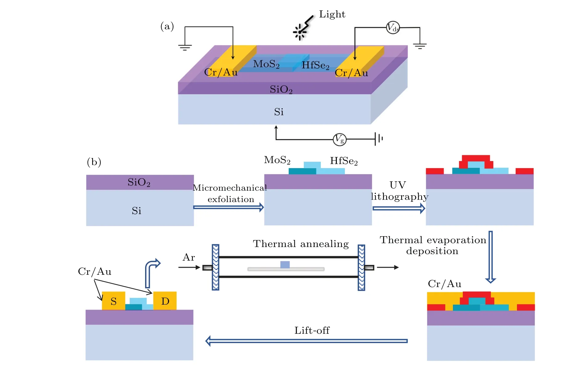
Fig.1. (a)Schematic view of the HfSe2/MoS2 phototransistor. (b)Diagram of the preparation processes of the HfSe2/MoS2 phototransistor.
3. Results and discussion
Figure 2(a)presents the optical image of the HfSe2/MoS2heterostructure. The smooth surface of the transferred 2D materials and the well surface morphology of the stacked heterojunction can be observed. The channel length (L) and width(W)of the phototransistors are measured at 5.9μm and 1.9 μm, respectively. Figure 2(b) shows the AFM image of the HfSe2/MoS2heterostructure. The flat and level of the surface morphology are more clearly observed. The inset shows the thicknesses of multilayer MoS2and HfSe2, which are estimated to be 18 nm(about 30 layers)and 32.6 nm(about 54 layers),respectively.
Figure 2(c) displays the energy band alignment diagram of the HfSe2/MoS2heterostructure. The bottom of the conduction band, the top of the valence band and the electron work function of HfSe2(MoS2) are approximately?5.2 eV(?4.2 eV),?6.3 eV (?5.4 eV) and?5.5 eV (?4.6 eV),respectively,[27–29]respectively. After HfSe2is in contact with MoS2, a staggered (type II) band alignment is formed. The offsets of the conduction band and the valence band are about 1.0 eV and 0.9 eV,respectively. The Raman spectra of multilayer HfSe2and MoS2as well as the HfSe2/MoS2overlapped region are shown in Fig. 2(d), which are taken at room temperature by using a 532 nm laser. The MoS2has two Ramanactive peaks located at 407 cm?1(A1g) and 382 cm?1(E12g).The interpeak separation or frequency difference between A1gand E12gis 25 cm?1. Compared to the frequency difference of 16 cm?1for single-layer MoS2,[30]our micromechanical stripping MoS2flake should be multilayer MoS2, which is in agreement with the thickness measured by AFM. The HfSe2shows a Raman-active peak located at 198 cm?1(A1g), and lacks Egpeak at 146 cm?1, which indicates that the HfSe2flake is multilayer.[31]All characteristic peaks of both MoS2and HfSe2are observed in the stacked region, implying good formation of a vdW heterojunction.

Fig.2. (a)Optical image,and(b)AFM image of the HfSe2/MoS2 heterostructure(inset: thicknesses of multilayer MoS2 and HfSe2 measured by AFM).(c)Energy band alignment diagram of the HfSe2/MoS2 heterostructure.(d)Raman spectra of HfSe2,MoS2,and their stacked region.
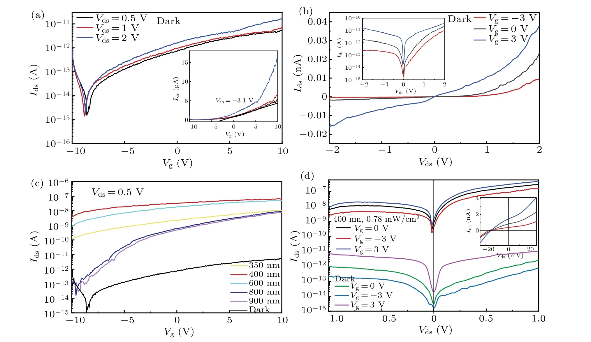
Fig.3. (a)Transfer characteristics of the HfSe2/MoS2 phototransistor under dark at Vds=0.5 V,1 V,2 V.The inset is shown on a linear scale.(b) Output characteristics under dark at Vg =0 V and ±3 V. The inset is shown on a semi-logarithmic scale. (c) Transfer characteristic at Vds=0.5 V under dark and different wavelengths with 0.78 mW/cm2. (d)Output characteristics at Vg=0 V and±3 V under dark and 400 nm illumination with 0.78 mW/cm2. The inset shows the output characteristics with the Vds from ?25 mV to 25 mV.
Figure 3(a)shows the transfer characteristics of the phototransistor under selected bias (Vds) of 0.5 V, 1 V, and 2 V,and the inset is shown on a linear scale. The threshold voltage(Vth)is extracted as?3.1 V from theIds–Vgcurve of the phototransistor atVds=0.5 V by the linear extrapolation method,which is marked in the inset of Fig.3(a). It can be seen from the structure of the device(see Fig.1(a))that the HfSe2/MoS2heterojunction is connected in series with HfSe2and MoS2,so the transfer characteristics of the device are also co-modulated by HfSe2and MoS2nanoflakes. When the back-gate voltage(Vg)is less than theVth(?3.1 V),the channel will be fully depleted and clamped off,resulting in the ultralow drain–source current (Ids). When theVgincreases from?3 V to 10 V, the channel gradually turns on and theIdsincreases sharply, indicating that the device has strong gating control effect. The output characteristics of the device for theVgof?3 V, 0 V and 3 V are shown in Fig. 3(b), and the inset is shown on a semi-logarithmic scale. An obvious gate-modulated rectifying behavior can be observed at theVgof?3 V and 0 V.The rectification factor is about 41 atVg=?3 V and|Vds|=2 V,and decreases to about 13 as theVgdecreases from 3 V to zero.However, forVg=3 V, the device does not display the rectification characteristic due to a large reverse current caused by the conduction of the channel at negative reverse bias.
Figure 3(c) shows the transfer characteristics of the device under dark and different wavelengths illumination with 0.78 mW/cm2atVds=0.5 V.The significant enhancement of the photocurrent can be observed for the NUV and visible light illumination. It has been reported that both multilayer MoS2and multilayer HfSe2have relatively strong light absorption from NUV to visible region,[3,32–34]which induces an increase of photogenerated carriers in the HfSe2/MoS2heterojunction,resulting in a significant enhancement of the photocurrent.Under the illumination of NIR,there is a slight increase in the photocurrent, which is related to the weak absorption tail of the indirect band gap semiconductors MoS2and HfSe2.[3,35,36]Figure 3(d)displays the output characteristics under dark and 400 nm illumination with 0.78 mW/cm2. In semi-logarithmic coordinate, it can be clearly observed that the HfSe2/MoS2heterostructure has strong photoresponse and ultralow dark current. Under zero bias, forVg=3 V, the dark current is about 3.09 fA and the photocurrent reaches 1.6 nA;while forVg=0 V, the dark current is as low as 1.8 fA and the photocurrent is as high as 0.9 nA;forVg=?3 V,the dark current is further reduced to 1.22 fA,and the light-dark current on/off ratio exceeds 105,indicating that the prepared heterostructure not only has an ultralow dark current, but also exhibits gate tunability for light-dark current. The output characteristics of the device with bias voltage from?25 mV to 25 mV are shown in the inset of Fig. 3(d). Under 400 nm illumination with 0.78 mW/cm2, the photovoltaic characeristics of the device can be observed. The short-circuit current(Isc)and opencircuit voltage (Voc) are 0.9 nA and 15 mV atVg=0 V, respectively, implying that the vertically-stacked HfSe2/MoS2heterostructure can also be applied to self-powered photodetection for the illumination of 400 nm. However, for other wavelengths of light,the photovoltaic effect of the phototransistor is very weak,especially for the illumination of 800 nm and 900 nm,and no photovoltaic effect is observed.
To further clarify the operation mechanism of the phototransistors based on the vertically-stacked HfSe2/MoS2heterostructure, simplified energy band diagrams are shown in Fig.4. As shown in Fig.4(a), in the absence of applied voltage and illumination, when the Cr/Au electrode is in contact with MoS2, a Schottky contact will be formed between them because the work function of the electrode is higher than that of the MoS2(4.6 eV).[29]On the other hand,the HfSe2has a high work function of 5.5 eV,[27,28]so the electrode will form a perfect ohmic contact with the HfSe2. Moreover, near the HfSe2/MoS2heterojunction contact interface, there is a stable built-in electric field pointing from MoS2to HfSe2. As shown in Fig. 4(b), under illumination, the built-in electric field can drive the photogenerated electrons and holes to drift in the opposite directions, forming a photogenerated current from MoS2to HfSe2and resulting in the generation of photogenerated electric field from HfSe2to MoS2. The direction of the photogenerated electric field is opposite to that of the built-in electric field,which is similar to adding a forward bias to the heterojunction, so the intensity of the built-in electric field is reduced. As a result,the current caused by carrier diffusion is greater than the drift current, thus generating a net forward current.
Figures 4(c)–4(e)show the schematic diagrams of simplified energy band under a forward bias and different back-gate voltages without illumination. ForVg=0 V,when a forward bias is applied, the built-in potential near the interface of the heterojunction will drop. As a result,only a small number of electrons with relatively high energy will move from MoS2to HfSe2to form a low dark current, as shown in Fig. 4(c).On the contrary,when a reverse bias is applied,the enhanced built-in potential barrier can effectively suppress the reverse current of the phototransistor, resulting in nonlinear rectification characteristic(see Fig.3(b)). If a positive back-gate voltage is applied, the quasi-Fermi level approaches closer to the conduction band, forming a lower Schottky barrier near the source end of the channel (see Fig. 4(d)) as compared to the state atVg=0 V (see Fig. 4(c)),[30]which contributes to the generation of a relatively high dark current (see the inset in Fig. 3(b)). Conversely, if a negative back-gate voltage is applied, the quasi-Fermi level is far away from the conduction band, resulting in a higher Schottky barrier near the source end of the channel (see Fig. 4(e)),[37]which further reduces the dark current (see the inset in Fig. 3(b)). Under illumination,the valence band electrons are excited to the conduction band,thus generating electron-hole pairs in MoS2, the depletion layer and HfSe2, as shown in Fig. 4(f). When a forward bias voltage is applied,the triangular barrier in the heterostructure will be lowered and narrowed,resulting in a large number of electrons to tunnel through the barrier.[16]Furthermore,the surface states of the electrode/MoS2interface can capture photogenerated carriers,which leads to the reduction of the Schottky barrier height.[38,39]Thus,the photogenerated charges can effectively move to the external circuit to generate a high photocurrent.

Fig.4. Simplified schematic energy band diagrams of the HfSe2/MoS2 phototransistor(a)under open circuit without illumination,(b)under short circuit and illumination,(c)under Vg=0 V and Vds>0 V without illumination,(d)under Vg>0 V and Vds>0 V without illumination,(e)under Vg<0 V and Vds>0 V without illumination,(f)under Vg<0 V,Vds>0 V and illumination.

Fig. 5. (a) Dependence of photocurrent on power density under 400 nm illumination at Vg =0 V and bias voltages of 0 V, 0.5 V, and 1 V,respectively. The dependence is fitted using Iph ∝Pα. (b)Responsivity(R),and(c)specific detectivity(D?)under different wavelengths with 0.78 mW/cm2 at Vg=0 V and bias voltages of 0 V and 0.5 V,respectively. (d)Dependence of R and D?on the back-gate voltage under 800 nm illumination with 0.78 mW/cm2 at Vds=0.5 V.
To study the relationship between photocurrent and illumination power, we measured the photocurrent of the phototransistor under 400 nm illumination with different power densities atVg=0 V and bias voltages of 0 V, 0.5 V, and 1 V,respectively,as shown in Fig.5(a). The experimental data can be fitted by the power law ofIph∝Pα, whereαis an exponent andPis the light power density.αis a key parameter to reveal the photocurrent generation mechanism, which can distinguish the photoconductive and photogating effects.[40,41]The fitted values ofαare 0.78, 0.72 and 0.65 atVds=0 V,0.5 V,and 1 V,respectively. For the HfSe2/MoS2heterostructure phototransistor, photoinduced carrier excitation mainly involves photoconductive effect, photovoltaic effect and photogating effect, but its photovoltaic effect is relatively weak(Isc/Voc=0.9 nA/15 mV).Based on the transfer characteristic curves in Fig.3(a),whenVg(0 V)>Vth(–3.1 V),the channel is at on state. Therefore,the value ofα<1 indicates that the photogating effect dominates the optical response.
The responsivity (R) and specific detectivity (D?) are critical parameters to evaluate the performance of a phototransistor. TheRindicates the photoelectric conversion efficiency of a phototransistor for light, which can be defined asR=Iph/(P·S), whereIphis the generated photocurrent,Pis the incident power density,andSis the effective photosensitive area of the phototransistor. TheD?shows the spectral detection rate of a phototransistor in unit surface area and unit bandwidth. The higherD?means the better sensitivity of the detector. It can be defined byD?=R·S1/2/(2e·Idark)1/2, whereeis the elementary charge andIdarkis the dark current.[25,42]Figures 5(b)and 5(c)show the calculatedRandD?of the phototransistor in the spectral range from 350 nm to 900 nm, respectively. AtVds=0.5 V andVg=0 V,theR(D?)improves from 38.7 A/W(3.79×1013cm·Hz1/2·W?1)to a maximum of 1.42×10³A/W (1.39×1015cm·Hz1/2·W?1) with the illumination wavelength from 350 nm to 400 nm, and then reduces to 30.8 mA/W(3.02×1010cm·Hz1/2·W?1)for 900 nm. The change trend is basically consistent with the spectral response of multilayer HfSe2and MoS2.[3,25]In the absence of applied voltage, the tendency of theR(D?)with wavelength is in accordance with that when the bias voltage of 0.5 V is applied,but theR(D?)decreases by more than an order of magnitude as compared to the calculated value atVds=0.5 V for the illumination of the same wavelength. For example,theR(D?)is 10.2 A/W(1.43×1014cm·Hz1/2·W?1)for the 400 nm illumination in the self-powered mode. Furthermore,for the illumination of 800 nm and 900 nm,theRdecreases to 0.71 mA/W and 0.15 mA/W, respectively, which is due to the weak photoelectron conversion of HfSe2and MoS2for the NIR. Although the HfSe2/MoS2heterostructure has relatively low responsivity in the NIR region,D?of the device can still achieve 9.94×109cm·Hz1/2·W?1and 2.08×109cm·Hz1/2·W?1with no external voltage.
Figure 5(d) illustrates the dependence ofRandD?on the back-gate voltage under illumination of 800 nm with 0.78 mW/cm2atVds=0.5 V.TheRincreases gradually with the increase of the back-gate voltage from?4 V to 5 V,which is consistent with the increasing trend of photocurrent with the back-gate voltage (see Fig. 3(c)). From Fig. 5(d), it can also be seen that theD?gradually tends to a saturation with the increase of the back-gate voltage. It is attributed to the rapid increase of dark current and the saturation of photogenerated current with the increase of the back-gate voltage(see Fig. 3(c)). The above results show that the HfSe2/MoS2heterostructure has an efficient gate tunability for theRandD?,which is especially helpful in improving the sensitivity of the NIR detection for the phototransistor operating in ultralow power consumption.
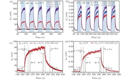
Fig.6. (a)Time-dependent photocurrent response of the phototransistor under switched-on/off illumination of 400 nm with 0.78 mW/cm2 at Vg =0 V and selected bias of 0.1 V, 0.5 V, and 1 V. (b) Time-dependent photocurrent response of the phototransistor under switched-on/off illumination of 400 nm for different power densities at Vg=0 V and Vds=0 V.(c)and(d)Rising and falling edges of one-cycle photoresponse under 400 nm illumination with 0.78 mW/cm2 at Vg=0 V and selected bias of 0.5 V and 0 V,respectively.
The transient photoresponse is also a crucial performance parameter for phototransistors. Figure 6(a) illustrates timedependent photoresponse under switched-on/off illumination of 400 nm with 0.78 mW/cm2atVg=0 V and bias of 0.1 V,0.5 V, and 1 V, respectively. A nearly identical response can be observed under periodically turning on and off light at each bias, demonstrating that the device has good stability and repeatability. Figure 6(b)exhibits obvious time-dependent photoresponse under switched-on/off illumination of 400 nm for different power densities without bias and the back-gate voltages.From Figs.6(a)and 6(b),it can also be seen that the generated photocurrent increases with increasing bias voltage and incident power density. Figures 6(c)and 6(d)show one entire on/off cycle of time-dependent photoresponse under 400 nm illumination with 0.78 mW/cm2atVg=0 V and selected bias of 0.5 V and 0 V,respectively. According to the time when theIdsincreases from 20% to 80% of the peakIdsand decreases from 80% to 20%, the corresponding response/recovery time of the phototransistor is 6.5 s/9 s (Fig. 6(c)) and 3.5 s/4 s(Fig. 6(d)), respectively. It shows that the time-dependent photoresponse of the phototransistor is relatively slow, but it is acceptable. The comparatively slow photoresponse may be mainly caused by the trapping effect and persistent photoconductivity effect.[43,44]When the phototransistor is illuminated, the photogenerated holes are captured in the traps located in thick HfSe2and MoS2,as well as at the interface of the two materials and maintained for a rather long time,which results in a long lifetime of the excited electrons in the conducting channel. Compared with zero bias,more electrons are attracted from the source into MoS2when a forward bias is applied,and the channel current eventually takes longer to increase to saturation.However,when the illumination is absent,a large number of induced electrons cannot quickly recombine with the trapped holes. Therefore,the response/recovery time atVds=0.5 V is greater than that atVds=0 V.A similar result has also been observed in photovoltaic photodetectors based on MoTe2/MoS2vertical heterojunctions.[23]
To demonstrate the performance improvement achieved by the HfSe2/MoS2heterojunction compared to the stateof-the-art 2D material counterparts, we summarize the key figures-of-merit, including responsivity, specific detectivity,and response/recovery time, as listed in Table 1. It is obvious that the devices we fabricated exhibit considerable good responsivity and specific detectivity.
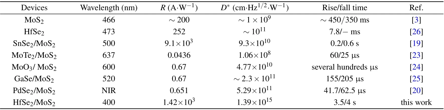
Table 1. Comparisons of the performance of phototectors based on related materials.
4. Conclusions
We successfully fabricate the HfSe2/MoS2heterostructure phototransistor based on the back-gate structure by the micromechanical exfoliation method. The device exhibits excellent photoelectric performance in a wide broadband ranging from NUV to NIR with/without external bias voltage and has an efficient gate tunability for light-dark current with on/off ratio above 105. At a bias of 0.5 V, it exhibits a high responsivity of 1.42×10³A/W and high specific detectivity of 1.39×1015cm·Hz1/2·W?1under 400 nm illumination of 0.78 mW/cm2. Moreover,the phototransistor can operate under zero bias with ultralow dark current of 1.22 fA,remarkable responsivity of 10.2 A/W,relatively high specific detectivity of 1.43×1014cm·Hz1/2·W?1, and acceptable response/recovery time of 3.5 s/4 s. These results should be attributed to the fact that the HfSe2/MoS2heterostructure not only improves the broadband photoresponse of the phototransistor but also greatly enhances its sensitivity. Therefore, the HfSe2/MoS2heterostructure phototransistor has potential applications in the fields of wide-spectrum response,self-driven photoelectric devices,and high sensitivity detection.
Acknowledgements
Project supported by the National Natural Science Foundation of China (Grant No. 51702245) and the Fundamental Research Funds for the Central Universities (Grant No.WUT2021III065JC).
猜你喜歡
當(dāng)代陜西(2021年18期)2021-11-27 09:01:20
Chinese Physics B(2021年11期)2021-11-23 07:29:20
遼寧省博物館館刊(2020年0期)2020-08-13 09:15:54
中小學(xué)校長(zhǎng)(2020年6期)2020-08-07 10:49:20
甘肅教育(2020年12期)2020-04-13 06:24:16
當(dāng)代陜西(2019年23期)2020-01-06 12:17:42
藝術(shù)品鑒證.中國(guó)藝術(shù)金融(2018年8期)2019-01-14 01:14:56
當(dāng)代陜西(2018年7期)2018-04-26 02:45:20
中國(guó)衛(wèi)生(2016年10期)2016-11-13 01:08:12
工業(yè)設(shè)計(jì)(2016年8期)2016-04-16 02:43:31

- Chinese Physics B的其它文章
- Fault-tolerant finite-time dynamical consensus of double-integrator multi-agent systems with partial agents subject to synchronous self-sensing function failure
- Nano Ag-enhanced photoelectric conversion efficiency in all-inorganic,hole-transporting-layer-free CsPbIBr2 perovskite solar cells
- Low-voltage soft robots based on carbon nanotube/polymer electrothermal composites
- Parkinsonian oscillations and their suppression by closed-loop deep brain stimulation based on fuzzy concept
- Temperature dependence of spin pumping in YIG/NiO(x)/W multilayer
- Interface effect on superlattice quality and optical properties of InAs/GaSb type-II superlattices grown by molecular beam epitaxy