
Stability,electronic structure,and optical properties of lead-free perovskite monolayer Cs3B2X9(B=Sb,Bi;X =Cl,Br,I)and bilayer vertical heterostructure Cs3B2X9/Cs3X9(B,B′=Sb,Bi;X =Cl,Br,I)
2022-02-24 08:59:06YaowenLong龍耀文HongZhang張紅andXinluCheng程新路
Chinese Physics B 2022年2期
Yaowen Long(龍耀文) Hong Zhang(張紅) and Xinlu Cheng(程新路)
1College of Physics,Sichuan University,Chengdu 610065,China2Key Laboratory of High Energy Density Physics and Technology(Ministry of Education),Sichuan University,Chengdu 610065,China3Institute of Atomic and Molecular Physics,Sichuan University,Chengdu 610065,China
The lead-free perovskites Cs3B2X9 (B=Sb,Bi; X =Cl,Br,I)as the popular photoelectric materials have excellent optical properties with lower toxicity. In this study, we systematically investigate the stable monolayer Cs3B2X9 and bilayer vertical heterostructure(B, B′ =Sb, Bi; X =Cl, Br, I) via first-principles simulations. By exploring the electrical structures and band edge positions, we find the band gap reduction and the band type transition in the heterostructuredue to the charge transfer between layers. Furthermore, the results of optical properties reveal light absorption from the visible light to UV region, especially monolayer Cs3Sb2I9 and heterostructure Cs3Sb2I9/Cs3Bi2I9, which have absorption peaks in the visible light region, leading to the possibility of photocatalytic water splitting. These results provide insights for more two-dimensional semiconductors applied in the optoelectronic and photocatalytic fields.
Keywords: first principles simulations, lead-free perovskite, monolayer Cs3B2X9, vertical heterostructure,photoelectric materials
1. Introduction
In recent years, lead-free perovskites have attracted widespread attention and interest due to their non-toxic and unique optoelectronic properties.[1—3]A large number of studies on 3D perovskites, such as Bi-based cesium bismuth halides,Sb-based cesium antimony halides,double perovskite semiconductor Cs2Sn1?xTexI6and Cs2AgxNa1?xInCl6powders,[1,4—6]have shown that they have well performance in photocatalytic water splitting, light-emitting diodes and solar cell applications.
Among those lead-free perovskites, Cs3B2X9(B= Sb,Bi;X= Cl, Br, I) compositions have been investigated as a promising material group due to their good properties. In 2019,Yousraet al.[7]reported that Cs3B2X9could be synthesized through dry mechanochemistry and showed white-light emission at room temperature through experiment. Moreover,first-principle studies of electronic and optical properties of Cs3Sb2X9revealed that the absorption red shifts from Cl to I as the band gap decreases.[4]Although 3D perovskites have experienced unprecedent rapid development in those years,their stability under the light and heat is still an important reason hindering their commercial applications.[8,9]Therefore,the corresponding two-dimensional perovskites have attracted more and more attention due to their excellent 2D quantum confinement effects.[10—13]The 2D halide perovskites are basically divided into two groups: inorganic layer and organic cation diversity. Lanzettaet al.[14]investigated the 2D organic tin halide perovskites (PEA)2SnIXBr4?xwith tunable optical properties in the visible spectrum by changing the I/Br ratio.Panet al.[15]investigated the layer-number-dependent electrical and optical properties of the all-inorganic 2D RP perovskite Cs2PbI2Cl2and emphasized that the excition-binding energy increases with the decreasing number of layers,which provides theoretical support to applications of 2D perovskites in photoelectric devices. In addition, we can also adjust the electrical and optical properties of perovskites by the composition, pressure or construction of heterostructures.[16—19]As mentioned above, lead-free perovskites based on Cs cation have been extensively studied, and the successfully synthesized 2D ultrathin few-layer(2—4 layers)Cs3Bi2I9provides a direction for the theoretical calculation.[20]In previous studies, there have not been systematic theoretical calculations for the two-dimensional monolayer Cs3B2X9perovskite, especially for stability of these substances.
In this article, we perform a systematic study of electronic, stability and optical properties of all-inorganic 2Dmonolayer Cs3B2X9via first-principles density functional theory. In Section 2, we give a comprehensive description of the calculation details. In Section 3, firstly we check the stability of monolayer Cs3B2X9(B= Sb, Bi;X= Cl, Br,I), secondly we study their electronic structures, thirdly we analyze the feasibility of their photocatalytic water splitting through the work function and optical absorption, fourthly stability, electronic and optical properties of the heterostructure(B,B′=Sb,Bi;X=Cl,Br,I)are discussed. Finally,in Section 4 we summarize all the results.
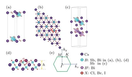
Fig. 1. (a), (b) and (d) Stereogram, top view, side view of the 2D monolayer Cs3B2X9,respectively,tagged with structure parameters. (c)The stereogram of heterostructure Cs3B2X9/Cs3X9 (B,B′ =Sb, Bi;X =Cl,Br,I).(e)The schematic diagram represents the Brillouin zone of the 2D monolayer Cs3B2X9 with high symmetric points Γ,M,K.
2. Computational details
All the calculations in this paper are based on firstprinciples density functional theory. Using the CASTEP[21]package for structural relaxation and phonon dispersions, we take different plane-wave cutoff energies from 400 eV to 750 eV to improve the computational efficiency for different systems and select the norm-conserving pseudopotentials. We utilize the approximation(GGA)represented by the Perdew—Burke—Ernzerhof(PBE)functional[22]to compute the phonon dispersions of the structure. The geometry optimization is finished when max ionic tolerance is lower than 0.03 eV/and the energy tolerances are less than 10?4per atom. We sample 2×2×1 grid ofk-point by Monkhorst—Pack scheme in Brillouin zone. The phonon dispersions are calculated by the linear response method.[23]
In order to further study more about these materials,we make some calculations about monolayer Cs3B2X9band structures using the Heyd—Scuseria—Ernzerhof (HSE06) hybrid functional since it is able to accurately calculate the band gap.[24]We also use it to get their work function and optical properties. Furthermore,we consider the effect of the van der Waals force using the DFT-D3 correction method of Grimme to compute the heterostructure(B,B′=Sb,Bi;X=Cl,Br,I).[25]Thek-point we make is 6×6×1 grid ofk-point by Monkhorst—Pack scheme in Brillouin zone and the energy (both total energy and band structure energy) change between two steps is smaller than 10?8eV. The plane-wave cutoff energy is set to 400 eV. All the calculations for this section are carried out using the Viennaab initiosimulation package(VASP).[26]
3. Results and discussion
3.1. Stability of monolayer Cs3B2X9 (B = Sb,Bi; X =Cl,Br,I)
Here we give a brief description of this structure. The 2D monolayer Cs3B2X9is a structure consisting of dioctahedraldimer-like units with corner-sharing connectivity surrounded by cesium cations (Fig. 1(a)). The vacuum layer between the upper and lower layers in thez-axis direction is about 20. The space-group symmetries of the monolayers Cs3B2X9are alland some of them are different from their 3D structures. For instance, the three-dimensional crystal structure of Cs3Bi2I9isP63/MMC.[27]
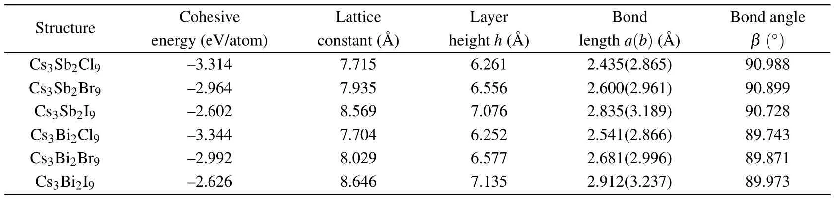
Table 1. The results for optimized geometries and cohesive energies of monolayer Cs3Bi2X9 obtained using DFT with PBE.
After the full structural relaxations,we obtain some structural information which included lattice constants,bond length and bond angle of monolayer Cs3B2X9as shown in Figs.1(a)and 1(d). The corresponding values are all listed in Table 1.To verify the stability of the monolayer Cs3B2X9structure,we perform calculations of the cohesive energy and calculations of the phonon dispersion. To calculate the cohesive energyEcohof monolayer Cs3B2X9,we use the standard formulawhereEtotis the total energy of monolayer Cs3B2X9,andEatomis the energy of each free atom, which is obtained by performing an isolated atom in a vacuum layer with a lattice constant of 15, avoiding the interaction between adjacent atoms. The cohesive energies listed in Table 1 are?3.314 eV(Cs3Sb2Cl9),?2.964 eV(Cs3Sb2Br9),?2.602 eV(Cs3Sb2I9),?3.344 eV(Cs3Bi2Cl9),?2.992 eV(Cs3Bi2Br9),?2.626 eV(Cs3Bi2I9). In the case of the same halogen atom, the absolute value of cohesive energy (see Table 1) of the monolayer Cs3Bi2X9is slightly higher than the monolayer Cs3Sb2X9, illustrating better stability of monolayer Cs3Bi2X9.
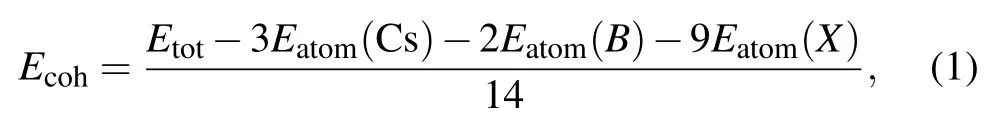
To further explore the stability of the monolayer perovskites Cs3B2X9,we execute the phonon dispersion. The results (Fig. 2) show that the lead-free monolayer perovskites Cs3B2X9in the Brillouin zone along a high symmetry point path (Fig. 1(e)) have fully positive phonon dispersion. The minimum acoustic branch near the gamma point is linear,meeting the expected results for the long-wave approximation,which demonstrates the dynamical stability of these monolayer Cs3B2X9compounds.
Combined with the above detailed analyses of the cohesive energy and phonon dispersion,we can conclude theoretically that the monolayer Cs3B2X9(B=Sb,Bi;X=Cl,Br,I)can exist stably.
Fig.2. (a)—(f)The phonon dispersion of Cs3Bi2Cl9,Cs3Bi2Br9,Cs3Bi2I9,Cs3Sb2Cl9,Cs3Sb2Br9,Cs3Sb2I9,respectively.
3.2. Band structures of monolayer Cs3B2X9 (B = Sb,Bi;X =Cl,Br,I)
Before exploring the heterostructure Cs3B2X9/Cs3B′2X9(B,B′= Sb, Bi;X= Cl, Br, I), the calculations of monolayer Cs3B2X9(B=Sb,Bi;X=Cl,Br,I)band structures are carried out using HSE06 hybrid functional (see Fig. 3). The bandgaps of monolayer cesium bismuth halides are 4.198 eV(Cs3Bi2Cl9), 3.564 eV (Cs3Bi2Br9), 2.874 eV (Cs3Bi2I9), as shown in Figs.3(a)—3(c), and the bandgaps of monolayer cesium antimony halides are 3.503 eV (Cs3Sb2Cl9), 2.981 eV(Cs3Sb2Br9), 2.476 eV (Cs3Sb2I9), as shown in Figs. 3(d)—3(f). Compared with the 3D crystal structure Cs3B2X9, the band gap of the monolayer structure is higher due to its 2D electronic dimensionality (quantum confinement effects),which can cause lower VB maximums(VBMs)and higher CB minimums (CBMs).[4,28]One can see that the Cs3Bi2X9type monolayer perovskites are all indirect bands with the VBMs occurring along theG—Mdirection and CBMs located atGpoint,as shown in Figs.3(a)—3(c). For Cs3Sb2X9-type monolayer perovskites,the similar pattern occurs except monolayer Cs3Sb2Cl9which VBM is located atG, and CBM appears betweenGandM. Comparing monolayer cesium bismuth halides and cesium antimony halides, we find about 0.5 eV more band gaps in V-group element bismuth. Therefore, the wide bandgap of Cs3Bi2X9can apply to high-power electronic devices and UV light devices. Furthermore,the band gap decreases as the weight of the halogen atom increases in both Cs3Sb2X9and Cs3Bi2X9, especially for Cs3Sb2I9with only 2.476 eV.This means that 2D monolayer Cs3Sb2X9has potential applications in visible light devices.
Kimet al.[16]reported that band gap increases as theB—Xdistance decreases in the crystal structure of Cs3B2X9,and the same features of monolayer structure show up (see Table 8).They also reported that the band gap increases as the electronegativity difference between theBsite metal andXsite halide increases, which is consistent with our present result(Fig. 3). However, the bond angleβ(Figs. 1(b) and 1(d))between two asymmetric atomsBrelative to central atomXshows an opposite trend in Cs3Sb2X9and Cs3Bi2X9. With the increase of band gap,the bond angleβof Cs3Sb2X9increases and the bond angleβof Cs3Bi2X9decreases.
To understand the contribution of each element and the electronic states of its different orbitals to the band, we perform calculations of total densities of states(TDOS)and partial densities of states(PDOS)of the monolayer Cs3B2X9near the Fermi level. Due to few contributions ofd-orbital of all elements to the electronic states near the Fermi level,we omit it when drawing,and the results are shown in Fig.4. The more details of DOS are placed in Appendix A.
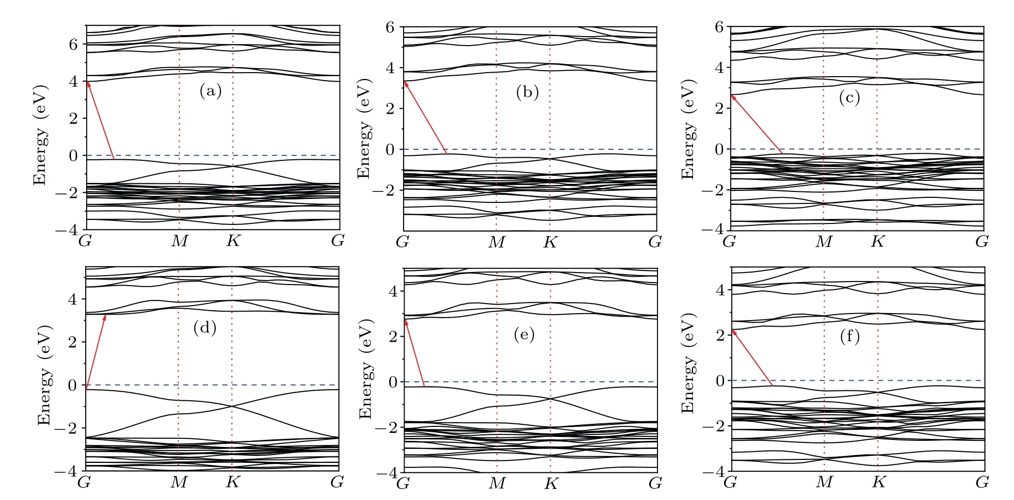
Fig. 3. (a)—(c) Band structures of monolayer Cs3Bi2Cl9, Cs3Bi2Br9, Cs3Bi2I9, respectively. (d)—(f) Band structures of monolayer Cs3Sb2Cl9,Cs3Sb2Br9,Cs3Sb2I9. The blue dashed line represents the Fermi level set to zero. The location of the band gap is indicated by the red arrows.
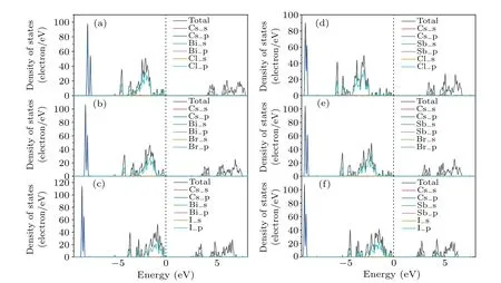
Fig.4. (a)—(c)TDOS and PDOS of the monolayer Cs3Bi2X9(X=Cl,Br,I),respectively. (d)—(f)TDOS and PDOS of the monolayer Cs3Sb2X9(X =Cl,Br,I).The black dashed line represents the Fermi energy level set to zero.
It is observed from the PDOS of all six types of monolayer Cs3B2X9that the state near the Fermi level has contributions from the s orbital ofB(Sb, Bi), the p orbital ofX(Cl,Br,I)andB(Sb,Bi). We can find that the states closest to the CBM of all monolayer Cs3B2X9have contributions from the p orbitals ofB(Sb, Bi) andX(Cl, Br, I). This suggests the existence of anti-bonding states due to the strong interaction between the p orbitals ofBandX. In the case of the state closest to the VBM,the contributions from the s orbitals ofB(Sb,Bi)and the p orbitals ofX(Cl,Br,I)imply a typical s—p interaction of the orbital hybridization ofB(Sb,Bi)andX(Cl,Br,I) atoms. In addition, the lower energy region of the valenceband is occupied by electrons in the p orbitals,indicating that the existence of bonding states due to the interaction between theB(Sb, Bi) and theX(Cl, Br, I) atoms. In general, with the increase of atomic number ofX(Cl, Br, I), the density of states near the Fermi level also increases, which provides convenience for the excitation of photogenerated carriers,suggesting its potential applications in optoelectronic devices.
3.3. Monolayer Cs3B2X9(B=Sb,Bi;X=Cl,Br,I)for water splitting

Fig.5. (a)Band edge position of monolayer Cs3B2X9 (B=Sb,Bi;X =Cl,Br,I)relative to the vacuum level(blue dashed line)calculated with HSE06 functional. The redox potential is marked with red dotted lines,and the legends B—X (B=Sb,Bi;X=Cl,Br,I)represent monolayer Cs3B2X9(B=Sb,Bi;X=Cl,Br,I).(b)The absorption spectra of monolayer Cs3B2X9.(c)The absorption spectra of monolayer Cs3Sb2Br9 and Cs3Sb2I9 before and after applying the mechanical biaxial strain.
As we all know, a good photocatalyst material needs a suitable band alignment. We have calculated the values of CBM and VBM via the hybridized functional HSE06 and determined the work function of the monolayer Cs3B2X9by calculating the vacuum level(see Fig.5).
In order to become an excellent candidate for the semiconductor material, the band edges must straddle the water redox potentials, which means that the VBM should be above the reduction potential (VH+/H2=?4.44 eV) and the CBM should be below the oxidation potential (VOH?/O2=?5.67 eV). As shown in Fig.5(a),almost all monolayer perovskites Cs3B2X9meet the requirement of the band alignment.However,the band gap of photocatalyst driven by visible light should be less than 3.0 eV (λ >415 nm).[29]Herein, the monolayer Cs3Sb2Br9,Cs3Bi2I9and Cs3Sb2I9,corresponding to the green,purple and brown lines in Fig.5(a),can be used as potential materials for visible light photocatalytic equipment.
In addition,we can see from the light absorption spectra(see Fig.5(b))that there are light absorptions in the visible region of Cs3Sb2I9and near-UV regions of Cs3Sb2Br9,Cs3Bi2I9monolayer lead-free perovskite,especially in Cs3Sb2I9,which shows an absorption peak in visible light region. Genget al.[17]have reported that the absorption edge of nanomaterial Cs3Bi2Br9exhibits a redshift with the increase of pressure,indicating a possible way to obtain the visible light absorption for monolayer Cs3Sb2Br9, Cs3Bi2I9. Furthermore, compared the changes in the light absorption coefficient of monolayer Cs3Sb2Br9and Cs3Sb2I9before and after applying the mechanical biaxial strain,it is seen that the red shifts occur with aη=6% compression (see Fig. 5(c)). This implies that the visible light absorption of monolayer Cs3B2X9can be achieved by applying an appropriate pressure.
3.4. Stability, band structure and optical properties for bilayer Cs3B2X9/Cs3X9 (B,B′ =Sb,Bi; X =Cl,Br,I)heterostructure
For the photocatalytic water splitting and photodetection,maintaining a long electron-hole recombination time is helpful for better detection and catalytic chemical reaction applications. The indirect band gap of monolayer Cs3B2X9must use the recombination center when conducting band electrons are recombined with valence band holes. Although the absorption efficiency is reduced in this process, the recombination time of electron-hole is prolonged (~ns) in contrast to some direct band gap materials(~ps).[30]In order to modulate the bandgap and obtain a longer carrier lifetime,two different twodimensional monolayer semiconductors are usually connected into a vertical heterostructure(HS).[31]Here,we can more easily combine Cs39(B′=Bi)and Cs3B2X9(B=Sb)to HSdue to their tiny mismatches of lattice constants,which are less than 1%.
We first calculate the binding energy of the heterojunction to investigate the structural stability. A standard formula of binding energy is given as follows:

whereEHSis the total energy of HS Cs3B2X9/Cs39(B,B′= Sb, Bi;X= Cl, Br, I), andElayer(Cs3B2X9),Elayer(Cs39)are the energy of the ground state monolayer Cs3B2X9(B=Sb;X=Cl, Br, I)and the ground state monolayer Cs39(B′=Bi;X=Cl,Br,I),respectively.The binding energies of HS (see Table 2) are?5.970 eV,?7.031 eV,?6.917 eV. Those are exothermic processes, indicating that the HS energy is reduced through the modulation of van der Waals forces.
Table 2. The parameters of HS Cs3B2X9/Cs3X9 (B,B′=Sb,Bi;X =Cl,Br, I) after structure relaxation using the PBE exchange-correlation functional.
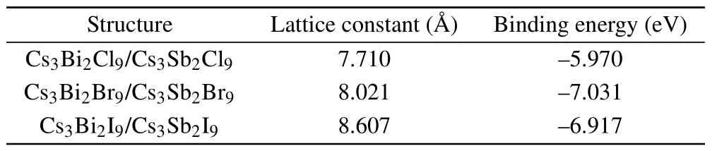
Table 2. The parameters of HS Cs3B2X9/Cs3X9 (B,B′=Sb,Bi;X =Cl,Br, I) after structure relaxation using the PBE exchange-correlation functional.
Structure Lattice constant(images/BZ_589_1417_292_1450_340.png) Binding energy(eV)Cs3Bi2Cl9/Cs3Sb2Cl9 7.710 —5.970 Cs3Bi2Br9/Cs3Sb2Br9 8.021 —7.031 Cs3Bi2I9/Cs3Sb2I9 8.607 —6.917
We next explore the band structures and density of states of the Cs3B2X9/Cs39(B,B′= Sb, Bi;X= Cl, Br, I),as shown in Fig. 6, with band gaps 3.133 eV (direct band),2.659 eV(indirect band)and 2.143 eV(indirect band). Compared to the monolayer Cs3B2X9, an obvious band gap decrease is found in the heterojunction,which implies an easier way for electron excitation from valence band to conduction band under the light. Moreover,the changing in band gap type of Cs3Sb2Cl9/Cs3Bi2Cl9can be explained through the PDOS and band structure, as shown in Figs. 6(a), 6(d), 6(g). The states near the VBM are occupied by the Cs3Sb2Cl9layer and the states near the CBM are occupied by the Cs3Bi2Cl9layer,which means that the excitation of electrons is energetically favorable from the VBM of Cs3Sb2Cl9(Gpoint in monolayer structure) to the CBM of Cs3Bi2Cl9(Gpoint in monolayer structure).
From the performed PDOS and band structures in Fig.6,it can be seen that all the three HS share the same trend that the VBM is dominated by the states from Cs3Sb2X9layer whereas the CBM is mainly provided by the states from Cs3Bi2X9layer. Furthermore, the valence band offset(VBO)and conduction band offset(CBO)between the Cs3Sb2X9and Cs3Bi2X9layers can be seen in Fig. 5(a), indicating the existence of the type II band alignment. Therefore, the transmission of photo-generated holes from Cs3Bi2X9to Cs3Sb2X9can be achieved through VBO and the electrons can be transferred from Cs3Sb2X9to Cs3Bi2X9powered by CBO.

Fig. 6. (a)—(c) Projected density of states (PDOS) and (d)—(i) projected band structures (PBANDS) of heterostructures Cs3B2X9/Cs3X9(B,B′=Sb,Bi;X =Cl,Br,I),respectively.
With the increase of the halogen atomic number of HS,it is observed that the states near the Fermi level are increased and give a narrower band gap (see Fig. 6). Unlike the alloyinduced phase transition,[27]Cs3Sb2I9/Cs3Bi2I9shows the most appropriate band gap for water splitting under the visible light, which is tuned by the charge transfer between layers,as shown in Fig.7(a). The type II band alignment caused by the interlayer electron excitation could adjust the electron transfer behavior as mentioned above to reduce the band gap.Photoinduced electron and hole transfers on different sides of the heterojunction promote charge-carrier separation to prevent rapid recombination of photogenerated carriers. Therefore, we explore the optical properties about heterostructure Cs3B2X9/Cs39(B,B′=Sb,Bi;X=Cl,Br,I).
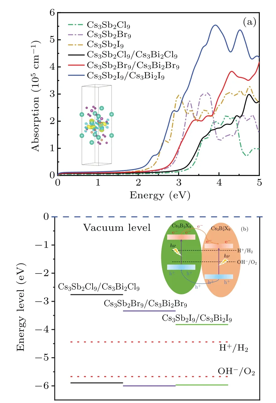
Fig.7. (a)Absorption spectra of Cs3B2X9/Cs3X9 and Cs3Sb2X9,the differential charge density of heterostructure Cs3Sb2I9/Cs3Bi2I9 (see inset). (b) Band edge position of heterostructures Cs3B2X9/Cs3X9 relative to the vacuum level (blue dashed line) calculated with the HSE06 functional,and the schematic of the band alignment(see inset).
The frequency-dependent dielectric function is calculated, and then the absorption coefficient as photon energy is evaluated. Compared with the monolayer structure, the heterostructures Cs3B2X9/Cs39show absorption redshifts in the visible region, see Fig. 7(a), which meet the reduction of band gap. The overall absorption of light is enhanced,while there are some small decreases in different photon energy ranges (~3 eV of Cs3Sb2I9/Cs3Bi2I9,~3.5 eV of Cs3Sb2Br9/Cs3Bi2Br9and~4 eV of Cs3Sb2Cl9/Cs3Bi2Cl9).They all achieve significant light absorption in the near-UV regions(for 3 eV—5 eV).However,only the Cs3Sb2I9/Cs3Bi2I9shows satisfactory visible light absorption. The difference of CBM could become the main reason to modify the light absorption, in the case of similar VBM, as shown in Fig. 7(b).In practical applications,substrates are often added to support and grow the materials.They could adjust the absorption coefficient via the internal distance between materials and the polar substrates.[32]Therefore,the selection of suitable substrate may provide an idea for further optimization of the absorption coefficient of heterojunction Cs3B2X9/Cs39.
4. Conclusions
In summary,we have theoretically investigated the structural stability, electronic structure and optical properties of monolayer Cs3B2X9(B= Sb, Bi;X= Cl, Br, I) and heterostructure Cs3B2X9/Cs39(B,B′=Sb, Bi;X=Cl, Br,I) based on first-principles calculations. The stability of monolayer structures is verified through cohesive energy and phonon dispersion, and the stability of heterostructures is checked by binding energy. For monolayer structures, the indirect band gaps from~2.5 eV to~4.2 eV and band edge positions warrant good light absorption in the visible and near-UV region, which can be adjusted by appropriate pressure to achieve the redshift of light absorption. For the heterostructures Cs3B2X9/Cs39,the band gaps from~2.1 eV to~3.1 eV reduction are observed due to the type II band alignment, which shows different states occupied in different layers near the CBM and VBM. Moreover, the changing of band type from indirect to direct atΓpoint is found in Cs3Sb2Cl9/Cs3Bi2Cl9due to a particular way of charge transfer between layers.The Cs3Sb2I9/Cs3Bi2I9shows satisfactory visible light absorption which is suitable for photocatalytic water splitting,while the other two show excellent absorption in near-UV region. The above results provide more options for photocatalytic applications of two-dimensional semiconductors.
Acknowledgements
This work was supported by the National Key R&D Program of China (Grant No. 2017YFA0303600), the National Natural Science Foundation of China (Grant No. 11974253),and the Science Specialty Program of Sichuan University(Grand No.2020SCUNL210).
Appendix A

Fig.A1. The DOS of different orbitals and elements of monolayer Cs3Sb2X9 (X =Cl,Br,I).

Fig.A2. The DOS of different orbitals and elements of monolayer Cs3Bi2X9 (X =Cl,Br,I).
猜你喜歡
Chinese Physics B(2024年3期)2024-03-25 09:30:16
Chinese Physics B(2023年1期)2023-02-20 13:15:46
Chinese Physics B(2022年9期)2022-09-24 08:01:22
廣西民族師范學(xué)院學(xué)報(2022年3期)2022-09-23 14:27:20
中國水土保持(2022年7期)2022-07-14 05:07:04
Chinese Physics B(2021年7期)2021-07-30 07:42:38
Chinese Physics B(2021年1期)2021-01-21 02:08:34
音樂天地(音樂創(chuàng)作版)(2019年6期)2019-09-20 05:53:50
鄉(xiāng)村地理(2018年2期)2018-09-19 06:44:04
中國衛(wèi)生(2015年6期)2015-11-08 12:02:38

- Chinese Physics B的其它文章
- A broadband self-powered UV photodetector of a β-Ga2O3/γ-CuI p-n junction
- High-sensitive terahertz detection by parametric up-conversion using nanosecond pulsed laser
- High efficiency,small size,and large bandwidth vertical interlayer waveguide coupler
- High-fidelity resonant tunneling passage in three-waveguide system
- An analytical model for cross-Kerr nonlinearity in a four-level N-type atomic system with Doppler broadening
- Determine the physical mechanism and source region of beat wave modulation by changing the frequency of high-frequency waves