
A double quantum dot defined by top gates in a single crystalline InSb nanosheet?
2021-12-22 06:41:04YuanjieChen陳元杰ShaoyunHuang黃少云JingweiMu慕經緯DongPan潘東JianhuaZhao趙建華andHongQiXu徐洪起
Chinese Physics B 2021年12期
關鍵詞:經緯
Yuanjie Chen(陳元杰) Shaoyun Huang(黃少云) Jingwei Mu(慕經緯) Dong Pan(潘東)Jianhua Zhao(趙建華) and Hong-Qi Xu(徐洪起)
1Beijing Key Laboratory of Quantum Devices,Key Laboratory for the Physics and Chemistry of Nanodevices and Department of Electronics,Peking University,Beijing 100871,China
2State Key Laboratory of Superlattices and Microstructures,Institute of Semiconductors,Chinese Academy of Sciences,Beijing 100083,China
3Beijing Academy of Quantum Information Sciences,Beijing 100193,China
Keywords: two-dimensional materials,InSb nanosheet,quantum dot
1. Introduction
Narrow bandgap InSb nanostructures with strong spin–orbit coupling(SOC)and large Land′eg-factor have attracted growing attention in the fields of spintronics and quantum information science and technology. Spin-based quantum states — especially in InSb quantum dots (QDs) — can be stored and manipulated by fast, efficient, and all-electrical means.[1,2]Two-dimensional(2D)multiple QD structures can not only be employed as building blocks for constructing semiconductor QD qubits[3,4]and quantum simulators,[5,6]but also help to read out[7,8]and braid[9,10]Majorana zero modes in semiconductor-based topological superconducting devices. However, advances in the realization and applications of QDs made from 2D InSb systems have been impeded due to the lack of an established fabrication technique. Charge instabilities,[11]gate hysteresis[12]and leakage problems[13,14]have limited the realization and investigation of high-quality, confined systems in heterostructured InSb quantum wells capped with thick buffer layers.[15–17]Very recently,single crystalline,zincblende,freestanding InSb nanosheets[18]have been grown via molecular beam epitaxy(MBE). Electrical measurements have shown that these freestanding nanosheets exhibit good transport properties and tunable, strong SOC, and are able to be contacted directly via metal deposition. In a recent report, experimental attempts to define a single QD in an MBE-grown freestanding InSb nanosheet have been made via top gate technique.[19]Although the signs of quantum confinement are observed in the transport measurements of the device, it is hard to achieve desired high-quality charge state stability diagrams and good controllability in the charge states of the QD defined in the InSb nanosheet,thus casting a serious question about whether these freestanding nanosheets could be employed to develop integrated QD devices for quantum information science and technology application.
In this paper, we report on the realization of a goodquality double QD (DQD) in an MBE-grown freestanding InSb nanosheet. The DQD confinement is achieved all by top finger gates,with a thin(10 nm)layer of HfO2as gate dielectric, using a gate layout optimized for InSb nanosheets. The fabricated devices are measured in a3He/4He dilution refrigerator with a base temperature ofT ~20 mK.Regular Coulomb diamonds are observed in the charge stability diagram of each individual QD,showing that the QDs can now be much better defined in the InSb nanosheet than that in Ref.[19]. The measured charge stability diagrams of the DQD demonstrate that the charge states and the inter-dot coupling of the DQD can be efficiently regulated by the top gates. We also perform a numerical simulation based on COMSOL program for the DQD.The results support our measurements and provide a better understanding of the fabrication and transport characteristics of the DQD made in the InSb nanosheet.
2. Experiment
2.1. Materials
The planar DQD device reported in this work is made from a free-standing,single crystalline InSb nanosheet. Freestanding InSb nanosheets are grown via MBE on top of the individual InAs nanowire stems on a Si(111)substrate. Prior to the growth process,a thin film of Ag is deposited onto the Si substrate in the MBE chamber and is annealedin situto form the Ag nanoparticles. With the use of these Ag nanoparticles as seeds,InAs nanowires are firstly grown on the Si substrate.By abruptly switching the group-V source from As to Sb and gradually increasing the supplied flux of Sb,freestanding InSb nanosheets are formed on the top of these InAs nanowires.The grown InSb nanosheets are investigated by scanning electron microscopy and transmission electron microscopy measurements. It is found that the morphology and size of the InSb nanosheets can be controlled by tailoring the Sb/In beam pressure ratio and growth time.It is also seen that these nanosheets are pure-phase zincblende crystals with flat surfaces,free from stacking faults,and of rhombic shapes with lateral sizes up to several micrometers and a thickness ranging from 10 nm to 80 nm. For further details about the growth and structural properties as well as basic transport properties of our MBEgrown InSb nanosheets,we would refer to Refs.[18,20,21].
2.2. Device fabrication and characterization
For device fabrication, the MBE-grown InSb nanosheets are mechanically transferred onto a heavily doped Si substrate(employed as a global back gate to fabricated nanosheet devices)with a 300-nm-thick capping layer of SiO2,and predefined metal markers on top. Subsequent to the nanosheet transfer,electron beam lithography(EBL)is carried out to define the source and drain contact regions on the selected InSb nanosheets. The metal contacts are then fabricated by means of electron beam evaporation (EBE) of 5-nm-thick Ti and 90 nm-thick Au, and a lift-off process. In order to obtain good contacts to the InSb nanosheets,the samples are wet etched in a de-ionized water-diluted(NH4)2Sxsolution at a temperature of 40?C for several minutes for the removal of the native oxide layer and for surface passivation in the opening regions of the InSb nanosheets before being loaded into the EBE chamber.Then the nanosheets are capsulated by a 10-nm-thick layer of HfO2(a top gate dielectric layer) through a combination of EBL,atomic layer deposition,and lift-off process. Finally,the patterned top gates are fabricated on top of the HfO2layer by a third step of EBL,followed by EBE of 5-nm-thick Ti and 90-nm-thick Au,and lift-off. Figure 1(a)shows the false-colored scanning electron microscopy image of a typical DQD device made from an InSb nanosheet with thicknesst ~30 nm.In the image,the scale bar is 500 nm,the source and drain,denoted by S and D,respectively,are colored in yellow,while the top gates, denoted by G1 to G6, respectively, are colored in light purple. Here,top gates G1 to G6 are all employed to provide electrostatic confinement to electrons in the InSb nanosheet.But,top gates G3 and G5 are also employed as plunger gates to control the chemical potential of the two individual QDs in the DQD, and top gate G4 is employed to tune the inter-dot coupling between the two individual QDs.Now,it is important to note that in a traditional 2D electron gas system made from a heterostructure with a thick cap layer, top gate electrodes are designed with a relatively large spacing between them to produce an appropriate confinement potential profile.[22,23]However, this might not be suitable for InSb materials with a very narrow bandgap (~0.23 eV). To realize complete depletion of electrons and at the same time prevent hole accumulation[24]in an InSb nanosheet,we have optimized the layout of top gate electrodes and the dielectric layer. On one hand, the dielectric layer should be thin enough such that a smaller negative gate voltage can deplete the local area of conducting electrons. On the other hand,the spacing between top gate electrodes should be narrow enough to provide sufficient confinement for electrons without the need of applying a large negative voltage. In this work, the spacing between gates G1 and G2 is designed to be 50 nm, and is the same as the one between gates G1 and G6. The small top gate spacing combined with a thin dielectric layer is essential for an accurate definition of electron confinement without inducing hole accumulation in an InSb nanosheet.

Fig. 1. Device structure and back-gate transfer characteristics (a) Falsecolored scanning electron microscope image of a typical DQD device studied by transport measurements in this work. The scale bar is 500 nm. (b)Measured source–drain current Ids at Vds=0.5 mV as a function of backgate voltage Vbg (the blue solid line)and the results of fit of the measurements to Eq.(1)(the red solid line).The yellow star marks the setting point of the back-gate voltage at Vbg =1 V for the rest measurements reported in this work.
The fabricated devices are measured in a3He/4He dilution refrigerator at a base temperature ofT ~20 mK. In order to improve the signal-to-noise ratio, electronic noises in the measurement circuits are minimized using a homemade copper-powder filter and a multiple RC filter set at different temperature stages. Below, we report the results of our measurements for the DQD device shown in Fig.1(a).
3. Results and discussion
3.1. Back-gate characterizations

3.2. Top-gate characterizations
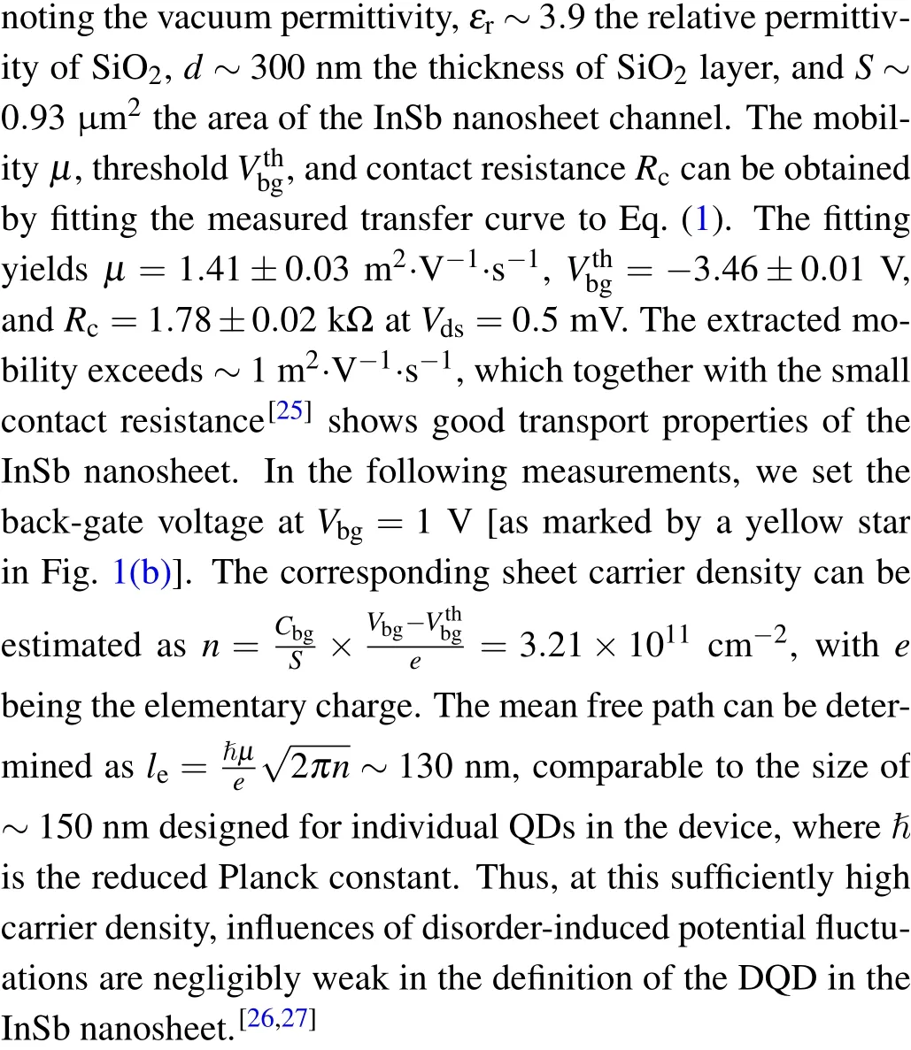
In this subsection,we determine the performance and setting point of the top finger gates in the device. Figure 2(a)shows the measuredIdsas a function ofVG1, i.e., the voltage applied to gate G1, atVds=0.5 mV andVbg=1 V, with all other top gates being grounded (i.e.,VG2–G6=0 V). AsVG1decreases from 0 V to about?0.5 V,Idsgets suppressed due to the depletion of the conducting carriers right beneath gate G1. WhenVG1continues to decrease,the currentIdssettles at an approximately constant value of~40 nA,indicating that the negative voltageVG1has totally depleted the carriers in the region covered by gate G1, but it nearly has no influence on the region which is not covered by gate G1. We then setVG1=?1.2 V[as marked by the yellow star in Fig.2(a)]and check the operating characteristics of other top gates. Figure 2(b)shows the measured currentIdsas a function ofVG2,i.e.,the voltage applied to gate G2,atVds=0.5 mV,Vbg=1 V,andVG1=?1.2 V, with all the remaining top gates being grounded. It is seen that the currentIdsgets pinched off atVG2=?0.75 V,showing that a quantum point contact(QPC)structure consisting of gates G1 and G2 functions efficiently to form a potential barrier to the conducting electrons in the nanosheet. In a similar way, the operating characteristics of the top gates G4 and G6 are evaluated. As shown in Fig.2(c)[2(d)], the measured currentIdsas a function of the voltage applied to gate G4(G6)approaches to zero atVG4=?0.53 V(VG6=?0.65 V),indicating that the formations of two QPCs,with one by gates G1 and G4 and the other one by gates G1 and G6,are achieved in the nanosheet. Note that the pinch-off voltages of the top gates G2, G4, and G6>?1 V, which are much smaller than these in Ref. [19]. This can be attributed to the thinner HfO2layer and optimized layout of the top gate electrodes. Based on these measured operating characteristics, in defining our DQD , we have set the voltages applied the three finger top gates atVG2=?0.74 V,VG4=?0.5 V andVG6=?0.63 V,which are slightly less negative than their own pinch-off thresholds in order to compensate the cross-talk effects of remote gates on these QPCs. The remaining top gates G3 and G5 are also characterized and are found to function properly. These two top gates are employed as plunger gates to the DQD. Note that the resonance-like fluctuation structures seen in all the measured current curves as shown in Fig. 2 are reproducible. Such fluctuations are commonly observed in the measurements of quantum devices made from free-standing semiconductor nanostructures,such as InAs and InSb nanowires. These fluctuations are inherent to a mesoscopic system in which the electron coherence length is on the order of the size of the conduction channel, and the electron mean free path is much shorter than the conduction channel size.[19]
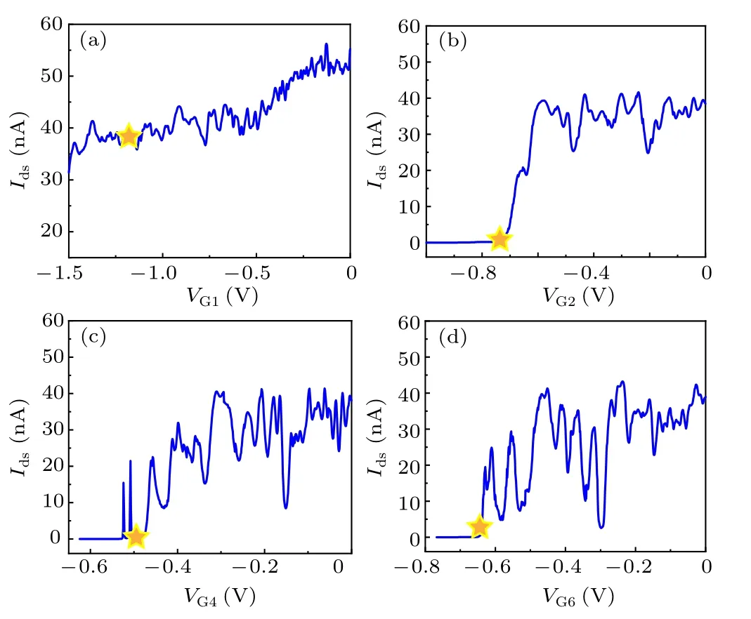
Fig. 2. Transfer characteristics of the top gates. (a) Measured Ids at Vds = 0.5 mV, Vbg = 1 V, as a function of VG1 with all other top gates grounded,i.e.,VG2–G6 =0 V.(b)Measured Ids at Vds =0.5 mV,Vbg =1 V,VG1 = ?1.2 V, as a function of VG2 with remaining top gates grounded,i.e., VG3–G6 =0 V. (c) The same as (b) but for Ids as a function of VG4 at VG1=?1.2 V,VG2=VG3=VG5=VG6=0 V.(d)The same as(b)but for Ids as a function of VG6 at VG1=?1.2 V,VG2–G5=0 V.The yellow stars in the four panels mark the setting points of the voltages applied to the these top gates,i.e.,VG1=?1.2 V,VG2=?0.74 V,VG4=?0.5 V,andVG6=?0.63 V.
3.3. Defining and transport characteristics of the DQD
In this subsection,we report our transport measurements of the DQD defined in the InSb nanosheet as described above.We firstly demonstrate the formation of two individual QDs which constitute the DQD. Figure 3(a) shows the measured currentIdsthrough the left QD,as defined in Fig.1(a)by setting top-gate voltages atVG1=?1.2 V,VG2=?0.74 V, andVG4=?0.5 V,as a function of the plunger gate voltageVG3at source-drain bias voltageVds=0.1 mV.Here,in the measurements, the top gates G5 and G6 are grounded, i.e.,VG5andVG6are set atVG5=VG6=0 V. Voltage applied to the back gate is always set atVbg=1 V through the entire measurements reported in this subsection. In Fig. 3(a), consecutive sharp current peaks (Coulomb current oscillation peaks) are observed over a wide range ofVG3, providing clear evidence of single electron transport through a QD in the Coulomb blockade regime.[28]Figure 3(c) shows the measured differential conductance dIds/dVdsof the left QD as a function of bias voltageVdsand gate voltageVG3(charge stability diagram). Here, we see a series of regular Coulomb diamond structures with closed degeneracy points at zero bias between neighboring Coulomb diamonds, indicating the formation of a well-defined single QD. It is also observed that the size of Coulomb diamonds(or the single-electron addition energy of the QD) shows a deviation from the regular even–odd effect,which has often been observed in the few electron regimes of a QD due to the spin degeneracy. This deviation is most likely due to the presence of double level degeneracy in our laterally defined QD.[29–32]In the following, this left QD formed by G1,G2,G3,and G4 is denoted as QD1. Figure 3(b)shows the measured currentIdsthrough the right QD (to be denoted as QD2),as shown in Fig.1(a)by setting the top-gate voltages atVG1=?1.2 V,VG4=?0.5 V,andVG6=?0.63 V,as a function of the voltageVG5applied to plunger gate G5 at source-drain bias voltageVds=0.1 mV.Here,the two uninvolved top gates G2 and G3 are grounded, i.e.,VG2=0 V andVG3=0 V are set in the measurements. The inset in Fig. 3(b) displays the zoom-in plot of two tiny current peaks in the gate voltage region marked by the red rectangle in the main figure. Clearly,the measured source–drain currentIdsexhibits Coulomb oscillations, i.e., signatures of single electron transport through a QD.Figure 3(d)shows the differential conductance dIds/dVdsmeasured for QD2 as a function ofVdsandVG5(charge stability diagram). Here, successive regular Coulomb diamonds are again observed,indicating that QD2 is well defined in the InSb nanosheet. Note that an extra,weak differential conductance line, marked by a yellow arrow in Fig.3(d), with a different slope from that of the boundaries of the Coulomb diamonds is observable. This line could most likely arise from a localized or impurity state formed unintentionally in a remote place from gate G5 and thus has a weaker coupling to the gate.[33]Note that the noticeable differences can be identified in the measured Coulomb current oscillations and charge stability diagrams of QD1 and QD2. These differences can be attributed to the differences in the sizes of confinement of the two QDs and indicate that deviations from our designed layout are present in our fabricated gate structures.
Fig. 3. Formation and characterization of two individual QDs. (a) Measured Ids as a function of VG3 at Vds = 0.1 mV for the left QD(QD1) in Fig. 1(a) defined by setting VG1 =?1.2 V,VG2 =?0.74 V, and VG4 =?0.5 V. The current oscillation peaks represent the single electron tunneling processes through QD1. (b)Measured Ids as a function of VG5 at Vds =0.1 mV for the right QD(QD2)defined by setting VG1 =?1.2 V,VG4 =?0.5 V, and VG6 =?0.63 V. The inset is the zoom-in plot of the region marked by a red rectangle in the figure. The current oscillation peaks represent the single electron tunneling processes through QD2. (c)Measured differential conductance dIds/dVds (in a logarithmic scale)as a function of bias voltage Vds and plunger gate voltage VG3 for QD1(charge stability diagram of QD1). The setup of the top gate voltages is the same as in(a). (d)Measured charge stability diagram of QD2. The setup of the top gate voltages is the same as in(b).The yellow arrow marks the appearance of an unintended differential conductance line as discussed in the text.

Fig.4. Charge stability diagrams of the DQD in three different inter-dot coupling regimes. (a)–(c)Measured Ids as a function of voltages VG3 and VG5 applied to plunger gates G3 and G5 (charge stability diagram) of the DQD, defined by setting VG1 =?1.2 V,VG2 =?0.74 V, and VG6=?0.63 V,in the three different inter-dot coupling regimes defined by setting VG4 at ?0.473 V,?0.42 V,and ?0.35 V,respectively. The yellow dashed lines in(a)mark the weak,nearly invisible horizontal current lines.
Having confirmed the two individually controllable single QDs, we now demonstrate the formation and transport properties of the DQD as defined in Fig.1(a)by settingVG1=?1.2 V,VG2=?0.74 V,VG4=?0.473 V,VG6=?0.63 V,andVbg=1 V. Figure 4(a) shows the measured source–drain currentIdsthrough the DQD at a source-drain bias voltage ofVds=0.1 mV as a function of plunger gate voltagesVG3andVG5(charge stability diagram of the DQD). It is seen that the charge stability diagram is featured by a chessboardlike pattern,[34]i.e., a group of relatively strong vertical current lines and a group of rather weak horizontal current lines(marked by horizontal dashed lines), and by small or hardly visible interactions between the two groups of current lines.The observation of these vertical and horizontal current lines indicates that plunger gates G3 and G5 address only effectively their own targeting QDs and have very small crosstalk capacitances to the other QDs. The weak interactions between the vertical and horizontal current lines indicate that the DQD is in the weak inter-dot coupling regime. Figure 4(b) displays the measured charge stability diagram of the DQD defined with the gate voltages all set the same as in Fig.4(a)except for the voltage applied to the inter-dot coupling gate G4 which has been set atVG4=?0.42 V.AsVG4increases from?0.473 V to?0.42 V, the coupling between the two QDs in the DQD and the crosstalk capacitances between the plunger gates and the QDs other than their locally addressing ones are enhanced.These enhancements lead to the appearances of finite slopes in the two groups of the current lines and of anti-crossing characteristics at the crosses of the two groups of the current lines.As a result,the current lines tend to show a honeycomb pattern in the charge stability diagram, see, e.g., a hexagon highlighted by the white dashed rectangle. In the lowest order transport process, the current flow occurs only at the corners, i.e., the triple points of the hexagons,[35]while the higher-order cotunneling processes give rise to the current observed at the boundaries of the hexagons.[34]Figure 4(c) shows the measured charge stability diagram of the DQD atVG4=?0.35 V,
where the DQD is in the strong inter-dot coupling regime.As shown in Fig. 4(c), the charge stability diagram is characterized by a series of diagonal current lines (with negative slopes), reminiscent of the formation of a large single QD.The bending of the straight current lines occurs when quantum levels in the two dots move close in energy. So far, we have demonstrated the realization of a DQD in our InSb nanosheet and that it is possible to tune the DQD from a weak inter-dot coupling regime to an intermediate and finally a strong interdot coupling regime with tuning plunger gate voltageVG4.
3.4. Simulation of the charge density and confinement potential in the DQD device
To get a better understanding of the formation of the DQD in the InSb nanosheet, we perform simulation for the charge density and electrostatic potential distributions in the system via finite element method by using commercially available program COMSOL.[36,37]Figures 5(a)–5(c) show the simulated 2D charge density profilein the InSb layer of the DQD system for the three experimental cases as seen in Figs.4(a)–4(c). In the simulation,the same layer structure and device layout as these in the experiment are employed.The average sheet carrier densityn2D=3.21×1011cm?2extracted from the measured back-gate transfer characteristics(i.e., theIds–Vbgcurve) is employed. The Fermi energy of the electrons in the conducting channel, free of the impact of the top gates, is then estimated asEF=nπ?2/m?≈51 meV, wherem?=0.014m0denotes the electron effective mass of InSb andm0is the mass of a free electron.The simulation starts with the determination of the spatial distribution of electric potentialφinside the InSb layer by using the three-dimensional (3D)Poisson’s equation

wheret=30 nm is the thickness of the InSb nanosheet and the integration is performed along the direction perpendicular to the InSb plane. Here, we define the direction perpendicular to the InSb plane as thez-direction, and thex–yplane is defined to be parallel to the InSb plane with thex-axis (yaxis) being along (perpendicular to) the direction of current flow. It is seen in Figs. 5(a)–5(c) that the simulation demonstrates good confinement of electrons by the top gates and thus the formation of the DQD in the InSb nanosheet. It is also seen that asVG4increases, the maximum charge density inside the DQD increases gradually from~2×1011cm?2to~2.4×1011cm?2and the charge population in the joint region between the two composite QDs increases from nearly zero to~1.5×1011cm?2. The results indicate that with increasingVG4, the couplings between the higher-energy electron states in the two QDs would become stronger.
Figures 5(d)–5(f) show the calculated electron potential energy eφalong the line cut ofy=0 andz=0, i.e., across the centers of the two QDs inside the InSb nanosheet,for the cases corresponding to Figs. 5(a)–5(c). The red dashed lines in the figures mark the Fermi energyEF~0.051 eV in the InSb layer. It is seen that the potential barrier height between the two QDs varies from~0.070 eV above the Fermi energy to~0.039 eV below the Fermi energy, giving an increase in coupling between QD1 and QD2 and thus supporting our experimental observation that the DQD has undergone a weakto-strong inter-dot coupling transition with increasingVG4.
4. Conclusions
In this work, a DQD device defined by optimized top gates is realized in an emerging high-quality,narrow bandgap,semiconductor InSb nanosheet. The fabricated device is studied by transport measurements in a3He/4He dilution refrigerator at a base temperature ofT ~20 mK.The charge stability diagrams are measured for the DQD in different inter-dot coupling regimes. It is shown that both the charge states and the inter-dot coupling of the DQD can be efficiently tuned by using the designed,dedicated top gates.Numerical simulation of the electrical potential and charge density distributions in the DQD have been performed and the results support the experimental observations and provide an insight into the structure design and performance of the DQD device. Our work sets a solid experimental step towards the development of laterally integrated semiconductor QD structures for quantum simulation and quantum computing.
猜你喜歡
現代城市軌道交通(2023年9期)2023-09-21 09:58:56
紡織機械(2023年5期)2023-08-21 10:30:00
紡織機械(2023年5期)2023-08-21 10:29:58
現代城市軌道交通(2022年11期)2022-11-21 04:21:22
China Textile(2022年3期)2022-07-12 05:37:36
兵團工運(2021年5期)2021-12-07 13:14:18
中國石油石化(2021年9期)2021-07-17 09:24:10
紡織機械(2020年1期)2020-05-20 13:29:14
集裝箱化(2018年2期)2018-04-03 08:26:36
中國工程咨詢(2017年1期)2017-01-31 02:55:52

- Chinese Physics B的其它文章
- Modeling the dynamics of firms’technological impact?
- Sensitivity to external optical feedback of circular-side hexagonal resonator microcavity laser?
- Controlling chaos and supressing chimeras in a fractional-order discrete phase-locked loop using impulse control?
- Proton loss of inner radiation belt during geomagnetic storm of 2018 based on CSES satellite observation?
- Embedding any desired number of coexisting attractors in memristive system?
- Thermal and mechanical properties and micro-mechanism of SiO2/epoxy nanodielectrics?