
Negative photoconductivity in low-dimensional materials?
2021-03-11 08:34:28BoyaoCui崔博垚YanhuiXing邢艷輝JunHan韓軍WeimingLv呂偉明WenxingLv呂文星TingLei雷挺YaoZhang張堯HaixinMa馬海鑫ZhongmingZeng曾中明andBaoshunZhang張寶順
Chinese Physics B 2021年2期
Boyao Cui(崔博垚), Yanhui Xing(邢艷輝), Jun Han(韓軍),?, Weiming Lv(呂偉明),Wenxing Lv(呂文星), Ting Lei(雷挺), Yao Zhang(張堯), Haixin Ma(馬海鑫),Zhongming Zeng(曾中明),?, and Baoshun Zhang(張寶順)
1Key Laboratory of Opto-electronics Technology,Ministry of Education,Department of Informatics,Beijing University of Technology,Beijing 100124,China
2Key Laboratory of Multifunctional Nanomaterials and Smart Systems,Suzhou Institute of Nano-Tech and Nano-Bionics,
Chinese Academy of Sciences,Suzhou 215123,China
Keywords: negative photoconductivity,low-dimensional materials,optoelectronic devices
1. Introduction
Negative photoconductivity (NPC), a phenomenon in which the conductivity of materials decreases under illumination, is uncommon because illumination normally generates additional carriers, which increase the conductivity of materials.[1]The NPC effect has potential applications in optoelectronic detection, optoelectronic switching, optoelectronic memory,gas detection,and so on.[2–7]For example,the NPC effect is helpful to expand the functions of traditional photoelectric detection and is expected to be applied to low-power,high-speed frequency response photodetectors.[8]Besides, its combination with the positive photoconductivity(PPC)effect can be designed into a photoelectric logic gate.[9]
The NPC effect is related to trap centers, surface gas molecules, and surface plasmons, etc., and mainly appears in bulk materials,[10–12]thin films,[13–16]and lowdimensional materials.[17,18]Among them, low-dimensional(including zero-dimensional[0D],one-dimensional[1D],and two-dimensional [2D]) materials have excellent physical and chemical properties, a large specific surface area, a high surface electron concentration,and abundant surface states.[19–22]Therefore,the low-dimensional materials are more conducive to the generation of traps,the adsorption,and desorption of gas on the surface of materials,as well as the excitation of the surface plasmons. Moreover,compared with thin film materials,the properties of low-dimensional materials are more easily regulated,and they can be made to have more excellent properties through chemical doping, physical adsorption, and surface decoration.[23–25]However,the role of the NPC effect in low-dimensional materials has not attracted the more attention of researchers, and the research is still in its infancy. In this review,first,we briefly introduce the PPC,and then we review reports about the NPC effect, systematically summarize the mechanisms to form NPC effect in existing low-dimensional materials,and outlook the future application prospect of NPC effect in low-dimensional materials.
2. The physical mechanism of PPC in lowdimensional materials
The physical effect of low-dimensional photodetectors are involved in the photovoltaic effect, the photoconductive effect, the photothermoelectric effect or the photobolometric effect, and the surface plasma-wave-assisted effect. Among them,the photoconductivity effect is that conductivity of semiconductor changes with the energy of incident light.[26]PPC is the phenomenon that conductivity increases under the incident of light. As is shown in Fig.1(b), under the irradiation of light, if the photon energy is greater than or equal to the forbidden bandgap, the semiconductor absorbs light and generates a mass of electron–hole pairs. Electron–hole pairs are separated and driven by the bias to form electrical signals.Meanwhile,carrier concentration increases,and resistance decreases, thus the conductivity and current increase. The conductivity(σ)of a semiconductor under light is made up of two parts: the dark conductivity(σ0)and the increased conductivity under light(?σ). The total conductivity can be written as
where μnand μpare the mobility of electron and hole, respectively. ?n and ?p are the increased concentration of the electron and hole under light,respectively.

Fig.1. Schematic model of forming positive photoconductivity without light(a)and with light(b). Reprinted(adapted)with permission from Ref.[27].
3. The formation mechanism of NPC in lowdimensional materials
3.1. The trapping effect
The formation process of the NPC effect caused by the trapping effect can be simply understood as the trap centers capture photo-induced carriers, causing the conductivity to decrease. The trapping effect is related to defects,[28]surface adsorbents,[29]and doping.[30]The NPC effect caused by the trapping effect can be applied to photoelectric detectors,non-volatile memories, and optoelectronic switches. In order to eliminate the influence of surface states in the research process, low-dimensional materials are usually tested in vacuum conditions or protected by inert materials, including oxide,polymer,core–shell structure.[31–34]In 2009,Panigrahi[35]studied ZnO quantum dots (QDs) in a SiO2matrix, in which NPC was observed, as shown in Fig.2(a). Hot electrons are trapped in the surface of ZnO, and free electrons are recombined with holes, so the NPC effect appears, as shown in the schematic model of Fig.2(b).In Fig.2(c),the response time of ZnO quantum dots detector is divided into two parts. The one part is the trapping process(faster time constant),as shown in the blue line. The other part is the carrier recombination process(slower time constant),as shown in the red line. Similar processes were also reported by Shahi[18]and Gogurla.[36]
The NPC effect has been reported in 1D materials, such as nanowire (NW), core–shell nanowire, nanorod (NR), and nanotube (NT). Yang[37]reported the spatially and spectrally resolved photocurrent studies of InAs nanowires, which revealed that the decrease in conductivity was caused by the trapping effect of light-induced hot electrons. The gain of the InAs nanowires photodetector reaches 105and the response time is less than 5 ms. Baek[30]observed the NPC in n-and pdoped Si nanowire field-effect transistors(FETs)and demonstrated the strong influence of doping concentration on the nonconventional optical switching of the devices. Hu[38]grew InAs core–shell-like nanowires by chemical vapor deposition(CVD), as shown in Fig.3(a). “Photogating layer (PGL)” is formed near the surface of nanowire, where there are many randomly distributed trap centers. As shown in Fig.3(b), the photogenerated electrons are trapped, and the holes remain in the core. In Fig.3(c), the remaining holes are recombined with free electrons. Besides, the trapped electrons generate a built-in electric field, further depleting free electrons in the core through the capacitive coupling,resulting in a decrease in conductivity. Shen[17]and Li[39]reported InAs core–shell nanowires respectively, and also attributed the NPC effect to the photogating caused by trapping effect. Ji[40]fabricated Ag/Al2O3hybrid nanorods. The NPC effect caused by the introduction of Ag can achieve the read–write–erase function,which could be applied to nonvolatile memory.Bergemann[41]reported a new C60 activated carbon nanotube (CNT) detector,which exhibits a high photoresponsivity of up to 108A/W,a detectivity of 1.6×10¹¹Jones(1 Jones=1 cm·Hz1/2·W?1),and a gain of more than 108. The device exhibits an NPC phenomenon and does not induce a change in threshold voltage.Incident light is absorbed by C60, and excitons are generated and then spread to the interface of C60/CNT.Due to the presence of the built-in electric field,electrons are transferred to C60, and holes are transferred to CNT. The electrons are trapped in trap centers, causing a change in the local electrostatic potential. These trap centers are also acted as the scattering centers of carriers,thereby weakening the conductivity.

Fig.2. (a)The I–V characteristic curves of ZnO quantum dots under ultraviolet and dark conditions. (b)Schematic model for the band diagram of the ZnO QDs-SiO2 composite showing the trapping of the charge carriers at the interface states under UV illumination. (c)The curve of photocurrent changing with time. The upper inset shows an instantaneous decline of the photocurrent with time. The lower inset shows the recovery process of the device. Reprinted(adapted)with permission from Ref.[35]. Copyright(2009)American Chemical Society.

Fig.3. (a)A schematic illustration of the InAs NW transistor. (b)The process of photogenerated electron–hole pairs. Under light illumination,electrons(e?)are excited into the PGL and keep trapped. Holes(h+)are left in the NW core. (c)The process of majority carrier dominated photodetection. Holes recombine with free electrons in the core. Electrons trapped in the PGL induce a photogating effect on the core.Reprinted(adapted)with permission from Ref.[38].
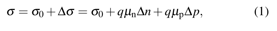
In 2D materials and its van der Waals (vdW) junctions,NPC caused by trapping is common. Fan[42]found that the hot carriers were captured by the trap centers in suspended WS2. In this work,the hot carriers easily overcome the energy barrier of the traps, so the response time is fast. While the electrons slowly cross the barrier in the recovery process,the recovery time lengthens. Niu[43]transferred NaYF4:Yb, Er quantum dots to 2D MoS2. The photogenerated electrons are captured by introducing NaYF4:Yb, Er quantum dots, showing the NPC effect caused by the trapping effect.Xie[44]found NPC in 2D Cr2Ge2Te6photoelectric detector under the 635-nm LED light, and PPC under the 635-nm laser irradiation.The difference between LED and laser is the intensity of light.The photocurrents(Iph)increase with the increase of light intensity.While the responsivities(R)of the detector under LED light and laser irradiation decrease with the increase of light intensity, because the absorption of light by materials reach saturation.[45–47]In this work,the responsivity of NPC is 105times that of PPC.It is conducive to weak light detection. Figure 4(a)shows the general photoresponse processes within the 2D Cr2Ge2Te6detector. Process 1 shows that some electrons on the valence band (Ev) absorb the photon energy and are excited to the conduction band (Ec), forming electron–hole pairs and leading to an increasing of carriers concentration.Process 2 shows that some electrons on the trap level(Etrap)are excited to the conduction band. Then in process 3, the lightinduced electrons recombined with the holes on the valence band, thereby reducing the carriers concentration. The total conductance is composed of two competing components: decreasing hole concentration caused by trap and recombination,and increasing hole concentration generated by light. When 2D Cr2Ge2Te6is exposed to weak LED light,the carriers are captured by trap centers, and the conductivity decreases after the recombination of carriers(see Figs.4(b)and 4(c)). In the other case, under the intense laser, the increase of the photogenerated holes surpasses the trapping effect. After recombination there are still a lot of holes,thus increasing the conductivity under the laser(see Figs.4(d)and 4(e)).
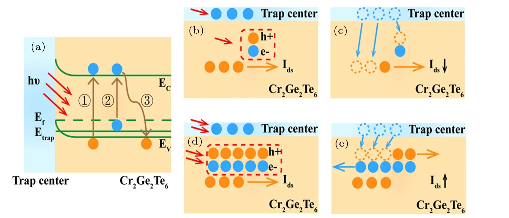
Fig.4. (a) Energy band diagram showing the general photoresponse processes within the 2D Cr2Ge2Te6 detector. (b)–(e) The schematic illumination of the NPC and PPC of the Cr2Ge2Te6 photodetector under the illumination of LED(b),(c)and laser(d),(e). Reprinted(adapted)with permission from Ref.[44].
Besides, defects could cause the trapping effect by capturing carriers. In 2019, Xiao[48]grew MoS2by CVD. NPC is found in the region of high defect density under the 660-nm laser irradiation,while PPC is found in the region of low defect density. This indicates that the occurrence of NPC is related to defect density. When defects are not considered,according to the PPC effect,a mass of electron–hole pairs are generated under the irradiation of light. As is shown in Figs. 5(a) and 5(b), the current increases. However, when defects are involved, some carriers are trapped by the trap centers caused by the defects. As is shown in Fig.5(d),in the region of high defect density,the decrease of carriers trapped in defects surpasses the increase of photogenerated carriers, inducing the NPC effect. Luo[49]found that the black phosphorus(BP)and BP/SnS0.5Se1.5van der Waals heterojunctions exhibited NPC in a positive gate range. It is due to the capture of photogenerated electrons in the defects.

Fig.5. Schematic model of forming positive photoconductivity without light(a) and with light (b) when defects are not considered. (c) In the region of low defect density, the small number of trapped carriers has little effect, so positive photoresponse occurs. (d) In the region of high defect density, the decrease of carriers trapped in defects surpasses the increase of photogenerated carriers,inducing the NPC effect.
Some optoelectronic devices based on the photogating effect exhibit gate-tunable photoconductivity, and play an important role in the study of the NPC effect. Under illumination,free electron–hole pairs are generated. If the electrons or holes are trapped in trap centers,the charged trap states can act as a localized floating gate and strongly modulate the channel conductivity,[27]which is called the photogating effect. If the trap centers capture the holes,the transfer characteristic curve shifts to the left.On the contrary,if the trap centers capture the electrons, the transfer characteristic curve shifts to the right.The magnitude of net photocurrent(Iph)can be expressed as

where gmis the transconductance. ?Vgis the horizontal displacement of the transfer characteristic curve, and it is also known as a local gate voltage. For example, as shown in Fig.6(a), if the photogenerated electrons are trapped, results in a right shift in the transfer curve (?Vg<0). Therefore,the difference value between the currents in the two transfer curves exhibits totally different: one part is positive, and the other part is negative. The optoelectronic device exhibit gate-tunable positive and negative photoresponse.In Fig.6(b),PPC appears at point A and NPC appears at point B.At point A, the majority carrier in dark is hole (gm<0), so according to the formula (2), PPC generates (Iph> 0). While at point B, the majority carrier in dark is electron (gm> 0),NPC generates(Iph<0). In summary, if the type of the photogenerated carriers injected into the channel is opposite to that of the majority carrier of channel material, or the type of the photogenerated carriers left in the gating layer or trap states is same to that of the majority carrier of channel material, then an NPC will be obtained.[53]Because carriers are trapped, the life of carriers are increased. Therefore, optoelectronic devices based on the photogating effect can greatly improve responsivity and gain.[51–53]The gate-tunable phenomenon of NPC caused by photogating has been reported in heterojunctions of BP/graphene(Gr),[54]rhodamine/Gr,[55]MoSe2/Gr.[56]Moreover,in 2D p–g–n heterojunction,the photogating effect is still applicable.Wang[57]fabricated MoS2/h-BN/ReS2van der Waals junction device, and Ahmed[58]prepared Gr/h-BN/MoS2heterojunction device. The above two reports mention that electrons can transfer between the floating gate and the conduction channel,which can be attributed to the photogating effect generated by the presence of defects.These electrons from the conduction channel would recombine with the holes trapped in the floating gate, thus the control of the floating gate over the conduction channel becomes weak.[57]So it leads to fewer accumulated electrons in the conduction channel,which results in the NPC effect.

Fig.6. (a)Ids–Vg trace shift after illumination. Dark line,red line,and blue line represent the dark current,photocurrent of photogating effect,photocurrent of photogating and photoconductive effect, respectively. (b) The I–V characteristic curves measured at A, B, and dark. Reprinted (adapted) with permission from Ref.[53].
3.2. Adsorption and desorption of gas molecules
The large specific surface area of low-dimensional materials is very conducive to the adsorption of gas molecules,and the gas molecules adsorbed on the surface have a significant influence on the current of a device.[59,60]Huang[61]found that NPC appeared in AlN nanowires when nanowires were irradiated by high energy photons. NPC and PPC could be converted to each other by changing the experimental environment(in the air or vacuum). Generally,there are two main explanations for the influence of gas molecules on the conductivity of materials: adsorption and desorption.
Zhuang[62,63]reported that NPC was generated when the graphene quantum dots (GQDs) were exposed to damp air. As shown in Fig.7, under the dark condition, the H2O molecule absorbs electrons in the GQDs,and result in a large p-conductance. Under illumination,photogenerated electron–hole recombine with each other,and the part recombined electrons come from H2O molecules,resulting in a disappearance of ionic conductivity and a decrease in total conductivity.With the increase in humidity,the NPC effect becomes more obvious. In further research, it is found that the NPC effect has a linear relationship with the concentrations of H2O,which is expected to be used in humidity detectors. In this work, the GQDs are only sensitive to ultraviolet light and are promising for ultraviolet photodetectors. Han[64,65]found NPC phenomenon in the study of InAs nanowires. An oxide layer with a large number of defect states is formed in the air. It reduces the mobility of carriers and decreases the conductivity by carrier scattering. Besides,in the surface of suspended graphene[66]and reduced graphene oxide (rGO),[67]O2and hydroxyl become scattering centers leading to the decrement of mobility. According to the formula: σ =μ×p (p is the concentration of hole),the conductivity decreases.
Fig.7. Schematic diagram of NPC caused by adsorption of H2O molecule in graphene quantum dots. Adapted from Ref. [62]; licensed under a Creative Commons Attribution(CC BY)license.
In 2001, Chen[68]found that the NPC phenomenon was related to the photodesorption of molecules (air, NH3, and NO2) when studying the single-walled carbon nanotubes.Fu[69]reported ceria (CeO2) nanowires, which showed NPC in humid air. Figure 8(a) shows the UV response of the ceria nanowires in air. As the desorption of molecules is a process that takes time, the device has a long response time. Figure 8(b) shows schematic representations of the ceria nanowires in response to UV illumination in air. H2O molecules are adsorbed to form hydroxyl groups and physically adsorbed to ceria nanowires by hydrogen bonds.According to Grotthuss’s chain reaction theory,[70,71]protons transfer between hydronium ions, forming surface ionic conductivity.Under the irradiation of ultraviolet light, due to the desorption of H2O molecules, the ionic conductivity fade away, the conductivity of nanowires decreases. In ZnSe:Bi nanowires,Zhang[72,73]elucidated the desorption mechanism of O2. It is similar to the desorption process of H2O.In addition,the desorption ability of molecules is related to photon energy. High energy ultraviolet has a strong capacity in desorption,[74–76]which can be used for cleaning nanowires,making nanowires chemical sensors have the rapid reversibility.[77–79]

Fig.8.(a)UV response of the ceria nanowires in air,exhibiting negative photoconductivity.(b)Schematic representations of nanowires in response to UV illumination in air. Reprinted(adapted)with permission from Ref.[69].
3.3. Surface plasmon resonance and surface plasmon polaritons
Surface plasmon resonance (SPR) is a physical-optical phenomenon. When the polarized light is incident at a specific angle (surface plasmon resonance angle), the reflected light is greatly reduced and the energy of the photon is transferred to the surface plasma. In 2009, on the alkane thiols structure, functionalized metal nanoparticles were assembled into the self-assembled monolayers (SAMs).[80]Organic ligands under the dark condition act as barriers. However,under irradiation,SPR causes the injection energy of the carrier to be 2 eV higher than that under dark,which makes organic ligands become effective trap centers. Carriers are trapped,causing a decrease in conductivity.In another report of NPC phenomena involving SPR,[1]it was found that SPR changed the electric field near metal nanoparticles. It is worth noting that the NPC phenomenon is not caused by the SPR, but by the trapping effect between the nanosheets and the nanoparticles.
Surface plasmon–polariton (SPP) is a transverse magnetic(TM)-polarized optical surface wave that propagates,for example, along a flat metal-dielectric interface, typically at visible or infrared wavelengths.[81]In this case, the photon does not interact directly with the electron but emphasizes the interaction between the SPP and the electron. In graphene nanotubes,[82]it was reported to produce quasi plasma-phonon particles as a part of the photogenic current. In this work, spolarized infrared light excites primarily the plasmon–phonon mode,while p-polarized light excites individual electron–hole pairs. The plasmon–phonon quasi-particle decays mainly through polar phonons into other phonons, while electron–hole pairs decay primarily into hot electrons.[81]This process finally increases the temperature of electrons and phonons,as shown in Fig.9. The increase in temperature leads to increasing scattering and decreasing conductivity. Sun[83]fabricated Ag nanowires and measured the properties of electrical and optical in a vacuum. The results show that the interaction between the SPP and the electrons under light produces additional scattering channels and reduces the current.A similar analysis was performed at the gold interdigitated electrodes.[15,84]The studies show that the precious metal films of nanoscale thickness exhibit significant negative photoconductivity due to light-induced SPP, which provides additional scattering channels for electron transport. It’s worth noting that SPP is related to surface roughness,and the results show that the increase of roughness leads to a decrease in the current.[85]

Fig.9. Illustration of the mechanism of phonon and hot electron generation through decay of the hybrid plasmon–phonon quasi-particles.Reprinted(adapted)with permission from Ref.[81].
3.4. The photobolometric effect
Different from the photothermoelectric effect,the photobolometric effect is related to photoinduced conductivity in the uniform light heating.[86–88]Photobolometric effect can affect the scattering of carriers and further affect conductivity. In 2017, Miao[89]obtained a flexible BP transistor on a polyimide film, as shown in Fig.10(a). Due to the poor thermal conductivity of the polyimide film,the increase of laser intensity leads to the rise of substrate temperature. In this case,phonons scattering results in the decrease of mobility and conductivity,as shown in Fig.10(b).Wu[90]reported that the negative photoelectric response of MoS2under near-infrared light.The photobolometric effect leads to lattice heating. Due to the interaction by scattering between phonons and electrons, the mobility and the conductivity of MoS2decrease. The phototransistor has a high optical response and a high speed(50 ms)and can be used for photoelectric detection, such as video image.[91]In an Au/Gr/p-type silicon heterojunction6,[92]it is found that the conductivity is modulated by the intensity of light. NPC appears under high light intensity,which is due to the photobolometric effect. It can raise temperature of device thus increase electron-phonon scattering. In addition,the conductivity affected by the photobolometric effect is related to the doping concentration. For example, in graphene,[93,94]a crossover shift from the photovoltaic effect to the photobolometric effect has been observed with increasing doping concentration because highly doped graphene can generate more scatterings.[95–97]

Fig.10. (a) Photograph of flexible BP FETs attached on a transparent polyethylene terephthalate(PET)handling substrate in its bending state. The schematic in the right inset shows the enlarged view of the flexible BP FET structure. (b) Device conductivity as a function of substrate temperature.The inset shows the deduced relationship between the incident laser intensity and device substrate temperature (293, 313, 333, 353, and 373 K).Reprinted(adapted)with permission from Ref.[89].Copyright(2017)American Chemical Society.
Besides, the NPC effect is also related to the desorption of surface molecules caused by the photobolometric effect.SnO2quantum dots grown on the graphene-skeleton have been observed negative photoelectric phenomenon.[98]A large η(η =Idark/Ilight) is demonstrated. It is found that the ultraviolet radiation and the direct heating almost have the same effect on resistivity. The irradiation of the laser for the device causes a temperature rise. As the temperature rises, the H2O molecules are desorbed, causing a decrease in surface conductivity. It is named pseudo-negative-photoconductivity(Psd-NPC). The experiment shows that the response time of the device is related to temperature,and the response time can be effectively reduced by using excellent heat dissipation materials. Psd-NPC can be used to make a logic circuit,which is expected to be used in transformers.
3.5. The trionic effect
A transient decrease in conductivity was observed in single MoS2.[99]This anomalous phenomenon is caused by the strong many-body interaction in a two-dimensional system, in which a photoexcited electron–hole pair is joined with a charge induced by doping to form a trion, which is a bound state of two electrons and a hole. It converts the 2D electron gas into a charged trion gas with the same charge density. The schematic of the trionic effect on the terahertz response is given. Absorption of terahertz (THz) pulse by the doping-induced free carriers is shown in the top part of Fig.11. The excitation of free electron–hole pairs could increase THz absorption,as shown in the middle part of Fig.11.While the formation of these trions reduces THz absorption.This is due to the fact that photoexcitation actually adds mass to the charges and dulls their response to the electric field,as shown in the bottom part of Fig.11. Compared with free electrons, trions allow us to control the motion of excitons. The optical properties and(pseudo)spin can be modulated through an applied electric field. It will lead to a very important application of the trionic effect in the field of spin devices and optoelectronic devices.

Fig.11.Schematic diagram of trionic effect on the terahertz response of a semiconductor under interband photo-excitation. Absorption of terahertz pulse by the doping-induced free carriers(the top part). Increased terahertz absorption by the excitation of free electron–hole pairs (the middle part). Reduced terahertz absorption by the formation of trions(the bottom part). Reprinted(adapted)with permission from Ref.[98].
3.6. Other NPC reports
In the literature, there are other explanations for the occurrence of the NPC effect. Some NPC phenomena appear in complex structures for a variety of reasons.[2,100]However,the multilayered structure leads to complex surface conditions,which are unfavorable for conductivity analysis. So here we only introduce some general cases with a simple structure.
In fact,we have mentioned hybrid structures in the above section and will introduce other reports about NPC in hybrid structures in the following. Researchers have found that 2D layered WS2/rGO hybrids show the NPC effect under the irradiation of infrared light.[101]Under dark, the holes flow and become background current, whereas WS2is not activated.When exposed to light, photogenerated electrons in WS2recombine with holes from rGO,resulting in a decrease in conductivity. A similar NPC has been found in the Gr/MoS2hybrid structure.[102]
In 2018, FePS3, a novel member of metal-phosphorustrichalcogenides, has been grown and tested.[103]When the negative gate voltage is applied,the Fermi energy level of the material moves toward the valence band,leaving more energy in the photoinduced holes. Higher mobility of the hole is observed, so the conductivity increases. On the contrary, under the positive gate voltage, lower mobility of the hole is observed, so the NPC appears. This is also a case where PPC and NPC are controlled by gate.
In the end,we summarized the reports about NPC in Table 1 (NUV=near ultraviolet, UV=ultraviolet, Vis=visible light,NIR=near infrared,IR=infrared). It is noted that some of the data in the table have been approximated for statistical purposes.

Table 1. Summary of NPC phenomena.
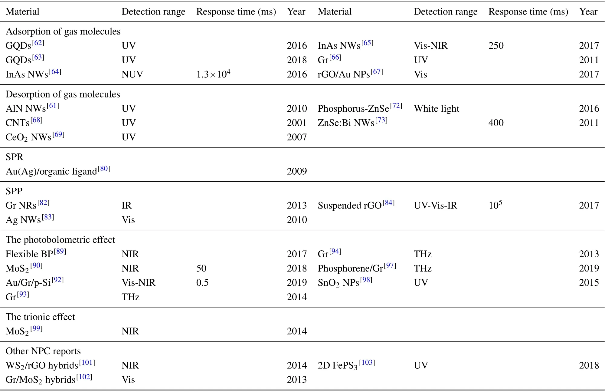
Table 1. (Continued).
4. Conclusion
In summary, this paper reviews the reports about NPC in low-dimensional materials and systematically summarizes the mechanisms for the formation of the NPC effect. Firstly,carriers are captured in the trap centers, causing the conductivity to decrease. NPC photodetectors induced by the trapping effect have high responsivity, which is suitable for the detection of weak light. Besides, the NPC effect can also be used in non-volatile memories. Secondly, charges can transfer between the material and the gas molecules during gas adsorption and desorption,thus weakening the conductivity.The NPC effect caused by gas adsorption and desorption can be used to clean low-dimensional materials and as gas detectors.Thirdly, NPC related to surface plasmons usually appears in cases where metal nanoparticles or electrodes are involved. It leads to enhancing scattering or additional scattering channels,thereby reducing mobility and conductivity.Fourthly,the photothermoelectric effect can also affect scattering and further affect conductivity. Besides, it affects the desorption process of gas and indirectly affects conductivity, which can be used in logic circuits. Fifthly,based on the strong many-body interaction in two-dimensional materials,a photoexcited electron–hole pair is joined with a charge induced by doping to form a bound state of two electrons and a hole. As the increased mass of the charge reduces their response to the electric field,NPC appears. Finally, other mechanisms are still in the process of study,and there is a large space for further study.
Based on the researches,it is found that the NPC effect is related to the defect density, wavelength, light intensity, concentration of O2and H2O, doping concentration, and other factors. High defect density can lead trap centers to capture more carriers and reduce conductivity.The wavelength of light also affects the NPC effect. The desorption effect of ultraviolet light on the surface gas molecules is stronger. The light intensity influences the conductivity by the quantity of carriers. If the quantity of carriers is too high, the scattering will be enhanced,which may lead to NPC.Conversely,if the quantity is too low, the decrease of carriers by the trapping effect surpasses the increase of photogenerated carriers, which may also lead to NPC.For gas molecules which may include but are not limited to O2and H2O molecules,they can be adsorbed on the surface of the material. The conductivity can be regulated by adsorption and desorption of gas molecules. Besides, the high doping concentration in the material affects the scattering of carriers,and further affects the photobolometric effect,resulting in the NPC effect.
At present, the NPC effect in low-dimensional materials can be applied in the fields of photodetection, logic circuit,memory devices, gas detection, cleaning of low-dimensional materials,and so on. Although the research on the NPC effect in low-dimensional materials is still in its infancy,it has shown great application potential, which provides a new perspective for the future study and application of low-dimensional materials.
猜你喜歡
Chinese Physics B(2022年10期)2022-10-26 09:47:54
現(xiàn)代職業(yè)教育·高職高專(2022年16期)2022-05-05 00:16:18
北方音樂(2020年23期)2020-12-24 01:07:32
當代工人(2018年24期)2018-03-29 08:10:10
意林·作文素材(2017年18期)2017-10-19 00:34:45
校園英語·上旬(2017年7期)2017-07-13 22:37:58
青春歲月(2017年6期)2017-05-13 13:20:45
——以新鄉(xiāng)學院為例
行政科學論壇(2016年7期)2016-10-25 07:10:46
延河(2016年1期)2016-02-26 08:21:46
語文知識(2015年11期)2015-02-28 22:02:03
- Chinese Physics B的其它文章
- Statistical potentials for 3D structure evaluation:From proteins to RNAs?
- Identification of denatured and normal biological tissues based on compressed sensing and refined composite multi-scale fuzzy entropy during high intensity focused ultrasound treatment?
- Folding nucleus and unfolding dynamics of protein 2GB1?
- Quantitative coherence analysis of dual phase grating x-ray interferometry with source grating?
- An electromagnetic view of relay time in propagation of neural signals?
- RF magnetron sputtering induced the perpendicular magnetic anisotropy modification in Pt/Co based multilayers?