
Ultraviolet photodetectors based on wide bandgap oxide semiconductor films?
2019-04-13 01:14:48ChangqiZhou周長祺QiuAi艾秋XingChen陳星XiaohongGao高曉紅KeweiLiu劉可為andDezhenShen申德振
Chinese Physics B 2019年4期
Changqi Zhou(周長祺),Qiu Ai(艾秋),Xing Chen(陳星),Xiaohong Gao(高曉紅),Kewei Liu(劉可為),and Dezhen Shen(申德振)
1State Key Laboratory of Luminescence and Applications,Changchun Institute of Optics,Fine Mechanics and Physics,Chinese Academy of Sciences,Changchun 130033,China
2University of Chinese Academy of Sciences,Beijing 100049,China
1.Introduction
In recent years,ultraviolet(UV)photodetectors have gained extensive attention of researchers worldwide owing to their potential applications in solar UV radiation detection,missile tracking, flame detection,ozone monitoring,environmental monitoring,etc.[1–4]Although GaN and SiC based UV photodetectors possess mature manufacturing technologies and thus have already been commercialized,[5–7]it is still tough to further reduce the cost and improve the performance for wide applications.Wide bandgap oxide semiconductors,including ZnO,ZnMgO,Ga2O3,TiO2,NiO,and so on,are the focus of current research efforts since they have special physical and chemistry properties,such as stability,environmental friendliness,and enrichment of raw materials.[8–12]Till now,the UV photodetectors based on wide bandgap oxide semiconductors with various device structures have been demonstrated,including p–n junction,Schottky junction,metal–semiconductor–metal(MSM)structure,and heterojunction.Several review articles have been published on ZnO-based UV photodetectors and metal–oxide nanostructure photodetectors.[13–17]Liu et al.summarized the history and the development of ZnO-based photodetectors.[13]Hou et al.[14]and Yang et al.[15]focused on the performances of ZnO-based UV photodetectors and the relevant physics.Zhai et al.[16]and Tian et al.[17]discussed several kinds of important metal–oxide nanostructures(such as ZnO,SnO2,Ga2O3,Cu2O,Fe2O3,In2O3,CdO,CeO2,Nb2O5,and WO3)and their corresponding photodetector applications.
In this review,we will first discuss the technical development of ZnO-based UV photodetectors,followed by recent advances of UV photodetectors based on Ga2O3,TiO2,and NiO.Finally,a brief summary,challenge,and prospect will be given.
2.ZnO-based film photodetectors
ZnO is one of the most prominent members of the family of wide bandgap oxide semiconductor due to its unique physical and chemical properties.[18–20]It has strong radiation hardness,high chemical stability,low cost,and a large bandgap of 3.37 eV at room temperature.[21–23]Furthermore,by alloying ZnO with MgO,the bandgap of ZnxMg1?xO can be adjusted from 3.37 eV to 7.8 eV,[24,25]which is essential to fabricate UV photodetectors with different cut-off wavelengths.These properties are crucial for practical optoelectronic devices used in missile warning system, flame detection,and inter-satellite communications.[26–28]In addition,ZnO and its alloy Zn-MgO materials are environment-friendly and rich in natural resources.Therefore,ZnO-based material is one of the best candidate materials for preparing UV photodetectors.[29–33]
After years of development,UV photodetectors based on ZnO and ZnMgO films have made great process,which has been discussed in the previous reviews.[13–15]Notably,to improve the performance of ZnO-based UV photodetectors,various methods have been selected,such as surface treatment,surface plasmonic effect,mixed-phase material,and so on.In this section,we will describe several ways to improve the performance of ZnO-based photodetectors.
2.1.Surface treatment
According to previous reports,ZnO exhibited a strong adsorption/desorption behavior of oxygen on the surface,which had a very big influence on the properties of ZnO-based UV photodetectors.[34,35]For example,these adsorption/desorption processes of oxygen on the surface of ZnO could lead to a long rise/decay time of bare ZnO-based UV photodetectors.[36,37]In order to improve the performance of ZnO-based UV detectors,scientists have studied many methods,such as oxygen plasma treatment,[38–41]surface passivation,[35,39,42]solution treatment,[43–45]and so on.In 2003,Coppa et al.[38]cleaned the ZnO(000-1)surface by O2/He plasma,which could significantly improve the rectifying characteristics of Au/ZnO junction.Liu et al.[46]treated the ultrathin(20-nm-thick)ZnO epitaxial films with oxygenradical-rich inductively coupled plasma to improve the performance of detectors (the decay time was reduced to below50μs and the on/off ratio was increased over 1000).In 2007,Angadi et al.[47]studied the effect of oxygen plasma treatment on the performance of Au–ZnO–In photodetectors,and a good Schottky junction detector with high UV responsivity(160 A/W at 254 nm)could be obtained after the treatment.In 2012,Reyes et al.[48]prepared a ZnO UV photodetector based on a thin film transistor(TFT),and the persistent photoconductivity of the device was suppressed through oxygen plasma treatment.Figure 1(a)shows the turn-off times of the untreated device,and the device with oxygen plasma treatment.The surface-treated device yields a reduced turn-off time of 10 ms as compared to 26 ms turn-off time of the untreated device.Figures 1(b)and 1(c)show O1speaks in x-ray photoelectron spectroscopy(XPS)spectra of the untreated ZnO channel and the O2plasma treated ZnO channel,respectively.The peak appearing at the lower binding energy 530.68 eV(OI)is due to the O2?ions presenting in the stoichiometric ZnO;on the other hand,the peak at the higher binding energy~532.38 eV(OII)could be attributed to O2?ions in oxygen deficient ZnO.The ratio of the peak area due to the oxygen deficient ZnO over the total area of the two peaks(OII/Otot)indicates the relative quantity of this oxygen-related defect.According to the results of XPS measurements,the improvement of recovery time for the photodetector is achieved through the suppression of persistent photoconductivity using oxygen plasma treatment to reduce the oxygen vacancies.
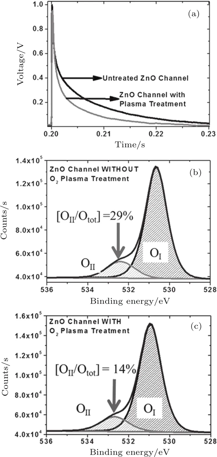
Fig.1.(a)Recovery times of the ZnO-TFT UV photodetector with and without channel surface treatment;XPS spectra of(b)untreated ZnO channel,and(c)oxygen plasma-treated ZnO channel.[48]
In addition to oxygen plasma,the surface treatment by solution is also a common method to improve the performance of ZnO-based photodetectors,and this method has been widely used in the devices based on ZnO micro/nanostructures.[49–52]Recently,scientists have introduced this method into ZnO thin film detectors.In 2017,Zhu et al.[36]investigated the effect of H2O2solution treatment on the properties of the ZnMgO thin film and its UV photodetectors.After the treatment by H2O2solution,the dark current of ZnMgO UV photodetectors decreased by more than one order of magnitude.Moreover,the response time of the device could be significantly reduced both in vacuum and an oxygen atmosphere by H2O2solution treatment due to the reduction in the oxygen vacancy defects in ZnMgO.However,the responsivity would also be obviously decreased using this method.
More recently,Chen et al.[37]demonstrated a performance enhancement of ZnMgO photodetectors through HF solution treatment.As shown in Fig.2,after the treatment with HF solution,the dark current decreases from 0.7 pA to 0.4 pA,and the peak responsivity of the device increases from 145 A/W to 326 A/W at 10 V.Additionally,the 90%–10%decay time of the device is decreased by more than one order of magnitude(from 4.6 ms to 0.34 ms).Large amounts of Zn–F or Mg–F on the ZnMgO surface should be responsible for the performance enhancement after HF treatment. The F-modified surface of ZnMgO film could adsorb more O2molecules and induce more oxygen-related hole-trap states due to the strong O2adsorption ability,resulting in low dark current and larger responsivity.Moreover,after turning off the UV light,the oxygen molecules are reabsorbed on the surface of ZnMgO and capture the free electrons more quickly,thus the smaller t-decay is achieved.This result indicates that the chemical treatment with HF solution should be a useful and effective method for improving the performance of ZnMgO UV photodetectors.
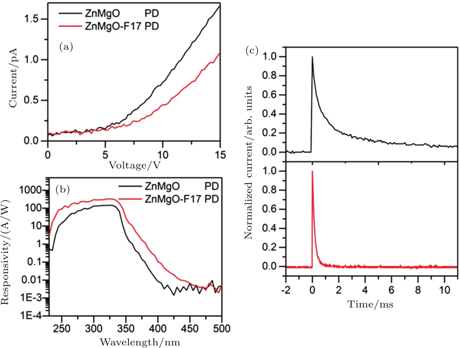
Fig.2.(a)I–V characteristics of devices in the dark.(b)Spectral responses of the devices under a bias of 10 V.(c)Decay edge of the current response at a bias of 10 V.[37]
2.2.Surface plasmonic effect
Surface plasmons(SPs)are collective oscillations of free electrons between metal and dielectric(semiconductor)materials,which have also been employed to enhance the performance of photodetectors.[53–64]
In 2014,Tian et al.[56]reported that Pt nanoparticles could be used to enhance the performance of the UV photodetectors,where surface plasma resonance occurs.Figure 3 shows the response spectra of the ZnO MSM structure UV photodetectors before and after sputtering of Pt nanoparticles.It can be seen that the responsivity of the device is enhanced from 0.836 A/W to 1.306 A/W by sputtering Pt nanoparticles on the surface of the device.After that,Pei et al.[57]demonstrated that the maximum responsivity enhancement ratio of ZnO MSM sandwich UV photodetectors could range from 14 to 45 times by adjusting the embedded depth of the Pt nanoparticles.In 2014,Li et al.[59]fabricated high-performance ZnO-based MSM UV photodetectors decorated with Ag nanoparticles by a chemical method positioned.After the introduction of the Ag nanoparticles,the responsivity of the device was enhanced from 472 mA/W to 51.3 A/W,but the dark current also increased.After that,their group reported the responsivity enhancement(from 472 mA/W to 10.522 A/W)of Ag nanoparticles-embedded ZnO film UV photodetector without the apparent increase of dark current.[60]In 2016,Sun et al.[61]fabricated ZnO semiconductor films with periodic 3D nanocave patterns,and the Au nanoparticles were subsequently introduced into the ZnO film,which could boost the UV responsivity and extend the photodetection to the visible light region.
Compared to the traditional dipole plasmon resonance,high-order plasmon modes are often excited in the shorter wavelength range,which is expected to be used to improve the UV-detection performance.Moreover,a highly wavelengths elective UV response enhancement for ZnO photodetectors could be achieved due to the narrow-band quadrupole resonance.In 2017,Ag nanoparticles-decorated ZnO photodetectors were proposed by Wang et al.,[62]and the device exhibited an obvious increase in peak responsivity at around 380 nm,which could be attributed to the narrow-band quadrupole plas-mon resonance of Ag nanoparticles in the UV range.Figure 4 shows the properties of UV photodetector based on ZnO thin film with and without Ag nanoparticles.The dark current of the device is decreased by the introduction of Ag nanoparticles.More interestingly,after covering with Ag nanoparticles,the intensity of the response peak increases obviously from 2.16 A/W to 2.86 A/W,while the responsivity at the other wavelengths decreases a lot,resulting in the full width at halfmaximum of response peak as narrow as~10 nm.Moreover,the response speeds of the ZnO UV photodetectors with and without Ag nanoparticles have no significant change.By coating Ag nanoparticles on the ZnO surface,a localized Schottky junction can be formed at the interface,and the wavelength of the ultraviolet light is coupled to the resonant frequency of the Ag nanoparticles.Thus,the performance of device could be enhanced obviously.This work would open a way to harness the high order plasmon modes in the field of UV optoelectronic devices.
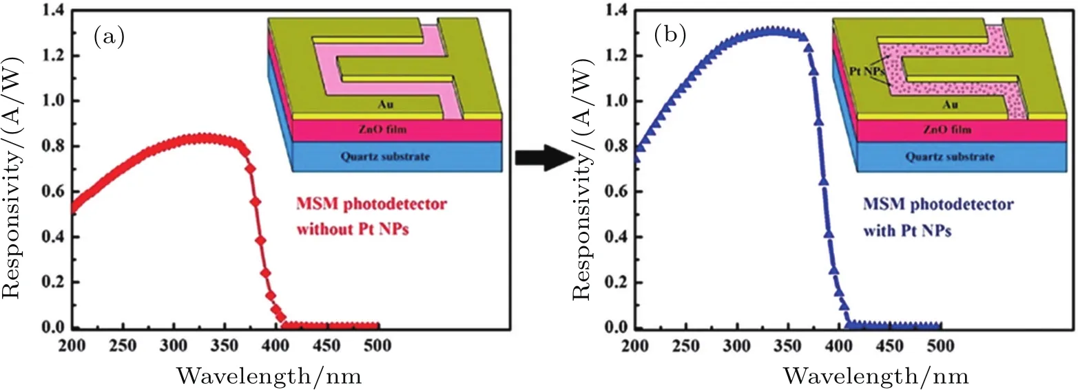
Fig.3.Response spectra of the ZnO MSM structure UV photodetectors before and after sputtering of Pt nanoparticles.The inset shows the schematic illustration of the device.[56]
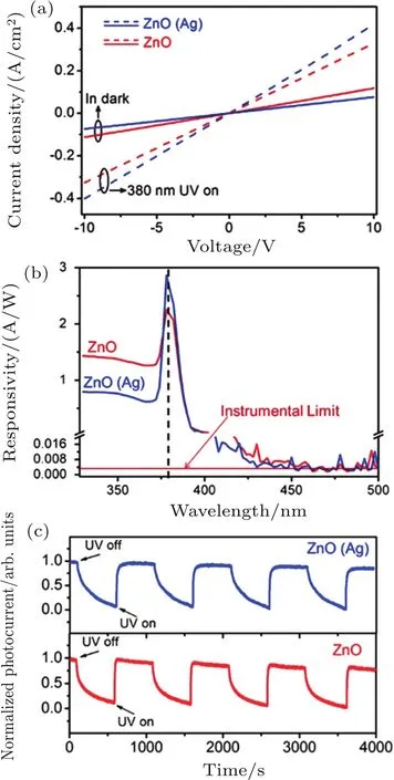
Fig.4.(a)J–V characteristics in dark condition and(b)response spectra of the ZnO UV photodetectors with and without Ag nanoparticles under 15-V bias.(c)Time-dependent photocurrent with periodic switching of UV illumination(380 nm)measured at 30-V bias.[62]
In brief,the performance of ZnO-based photodetector has been significantly improved by introducing metal plasm on resonance,and these results could provide a promising way to develop high-performance UV photodetectors.
2.3.Mixed-phase material
As is well known,ZnO is stabilized in the hexagonal wurtzite structure,while MgO is stabilized in the cubic rock salt structure.Therefore,the crystal structure of ZnMgO alloy would change from wurtzite structure to cubic structure as the Mg content increases.And ZnMgO with both hexagonal and cubic phases is commonly obtained in the previous reports,which could be called mixed-phase ZnMgO.It could be found that the photodetectors fabricated on mixedphase ZnMgO exhibit a relatively higher responsivity than that of the single-phase devices.[31,65,66]Thus,preparing mixedphase material may be a viable method to improve the performance of ZnMgO UV photodetectors.However,the mixedphase ZnMgO usually has two absorption edges: one is shorter than 280 nm and the other is longer than 300 nm,indicating that they are not suitable for solar-blind detection without external filters.[18,67–70]
In 2014,a mixed-phase Zn0.38Mg0.62O film with a single absorption edge has been firstly deposited on a-face sapphire using plasma-assisted molecular beam epitaxy by Fan et al.[71]Furthermore,a mixed-phase ZnMgO UV photodetector with excellent comprehensive performance has been fabricated.The device showed only one response peak at 260 nm with the responsivity of 1.664 A/W which is differ-ent from other mixed-phase ZnMgO photodetectors containing two photoresponse bands.In addition,the dark current of the device was only 0.25 pA at 5 V,which was much lower than that of the reported mixed-phase ZnMgO photodetectors.After that,Fan et al.further studied the carrier transport process of mixed-phase ZnMgO photodetector at different conditions,such as thermal equilibrium,dark,and UV illumination,as shown in Fig.5,[72]and tried to find out the reason for the excellent optoelectrical characteristic for the devices.They found that large amounts of heterojunctions between wurtzite-phase ZnMgO(w-ZnMgO)and cubic-phase ZnMgO(c-ZnMgO)in the mixed-phase ZnMgO film should be responsible for the ultra-low dark current;meanwhile,the high-resistance of c-ZnMgO film also plays an important role in producing low dark current.Under the radiation of UV light,photogenerated holes were trapped at the interfaces between w-ZnMgO and c-ZnMgO,prolonging their lifetimes.At the same time,the barrier height at grain boundary can be reduced,enhancing the electron conductance and reducing the electron-transit time. The longer lifetime could increase the internal gain and then increase the responsivity.After this study,some scientists began to focus on the mixed-phase ZnMgO UV photodetector.Han et al.[73–75]fabricated MSM structure UV detectors based on mixed-phase ZnMgO thin films by pulsed laser deposition(PLD)method,and the effect of the substrate surface atom constitution and the migration characteristics of reactive atoms on crystal structure of the ZnMgO thin films have been investigated.
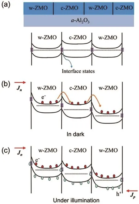
Fig.5.Energy band diagram and carrier transport process of mixedphase ZnMgO photodetector at different conditions:(a)at thermal equilibrium,(b)under bias in dark,and(c)under bias with UV illumination.[72]
In addition,several other methods have been used to improve the performance of ZnO-based UV photodetectors.[76–85]For example,Tian et al.and Wang et al.[82,83]developed the high performance ZnO nanosheet field-effect transistor by using ferroelectric to get the very low dark current.The device reveals an improved optical response and detectivity up to 3.8×10⁵A/W and 4.4×10¹⁵Jones(unit Jones:cm·Hz1/2·W?1),and the photocurrent gain is 1.24×10⁶.At the same time,Wang et al.[84]fabricated a high performance ZnO nanosheet photodetector driven by the charge transfer induced local field.The photodetector exhibits ultralow dark current(10?12A),ultra-high specific detectivity(up to~1014Jones),and fast rising(300 ms)and decaying times(310 ms).
Due to space limitations,we only summarize the above methods used to improve the performance of ZnO UV photodetectors(PDs).Although ZnO-based UV photodetectors have made great progress in recent years,there are still some problems remaining to be solved.For example,the lack of stable and reproducible p-type ZnO-based materials,the low responsivity of MgZnO solar-blind PDs,the slow response speed,and so on.Therefore,more research should be performed to address these challenges.
3.Ga 222O 333-based film photodetectors
Solar-blind UV photodetectors can accurately response to a very weak signal even under sun or room illumination.Monoclinic Ga2O3(β-Ga2O3),with an intrinsic bandgap Egof~4.9 eV and accordingly a corresponding wavelength of~ 260 nm,[86–91]is naturally suitable for solar-blind UV detection.Consequently,Ga2O3has attracted much attention recently,and its characteristics of solar-blind UV detection have been demonstrated in various device structures,including MSM structure,Schottky junction,and heterojunction structure.[92–103]
3.1.MSM structure
MSM structure photodetectors have the advantages of simple structure,easy preparation,etc.In 2007,Kokubun et al.[104]grew β-Ga2O3MSM photodetectors using sol–gel method,and the maximum responsivity of the device was only 8×10?5A/W.In2014,Guoetal.[105]depositedβ-Ga2O3epitaxial thin films using laser molecular beam epitaxy(L-MBE)technique,and in situ annealing on the film under oxygen atmosphere could lead to the transition of the Au/Ti electrode/β-Ga2O3thin film from ohmic to Schottky contact due to the reduction of the oxygen vacancy.Figure 6 shows the time dependent photoresponse of the β-Ga2O3thin films prototype photodetector to 254-nm illumination.The dark current,rise time,and decay time for the Schottky type photodetectors are only 0.3 nA,0.62 s,and 0.83 s,respectively.Compared with the Ohmic-type photodetector,the Schottky-type photodetector shows lower dark current,higher photocurrent/dark current ratio,and shorter switching time,which benefit from Schottky barrier controlling electron transport and the significant reduction in the quantity of photogenerated carriers trapped by oxygen vacancy.
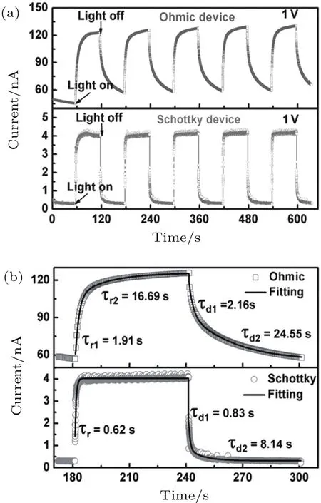
Fig.6.Time-dependent photoresponse of the β-Ga2O3thin films prototype photodetector to 254-nm illumination:(a)the ohmic-type device and the Schottky-type device;(b)enlarged view of the rise/decay edges and the corresponding exponential fitting for the ohmic-type device and Schottky type devices,respectively.[105]
In 2015,Hu et al.[106]deposited β-Ga2O3film using metalorganic chemical vapor deposition(MOCVD)technique,and the photodetectors with interdigitated electrodes have been designed and fabricated on this film.The device exhibited a responsivity of 17 A/W,a UV-to-visible rejection ratio of 8.5×10⁶,and a quantum efficiency of around 8228%at 20-V bias.In 2017,Alema et al.[107]reported the fabrication and characterization of solar-blind photodetectors based on undoped β -Ga2O3and Zn-doped β -Ga2O3(ZnGaO)epitaxial films with a cutoff wavelength of 260 nm.The ZnGaO detector showed a peak responsivity of 210 A/W at 232 nm,which is much higher than that for β-Ga2O3device(46 A/W).In 2018,Zhang et al.[108]grew high quality β-Ga2O3film by using N2O as reaction gas for the fabrication of high performance solar-blind photodetector.This device exhibited a high responsivity of 26.1 A/W.And the rise and decay times were around 0.48 s and 0.18 s at 10 V,respectively.The excellent performance can be attributed to the reduction of scattering or/and trapped center of photo-generated carriers formed in the film grown with N2O.
3.2.Schottky junction
Considering the potential applications in secure communication and space detection,the quick response speed and the self-powered ability for a solar-blind photodetector are strongly desirable.The vertical Schottky photodiode should satisfy this requirement.In 2016,an Au/β-Ga2O3nanowires array film vertical Schottky photodiode was successfully fabricated by a simple thermal partial oxidation process.[109]The device had a four-layer structure,namely,Au/β-Ga2O3nanowires array/β-Ga2O3film/Ga.This Schottky type photodetector showed an obvious solar-blind response without any power supply,and 90%–10%decay time is only 64μs.
3.3.Heterojunction structure
Weng et al.[110]reported the fabrication of a β-Ga2O3/GaN dual-band photodetector.The dark current of the device was only 3.58×10?11A at 5-V applied bias and the near-UV to visible contrast ratio was 850 at 10-V bias.In 2016,Guo et al.[111]fabricated β-Ga2O3thin films on p-type silicon(100)substrates by laser molecular beam epitaxy,and the heterojunctions were then formed as a deep UV solarblind photodetector.The responsivity of the device reached 370 A/W at 3 V reverse bias at 254 nm,and the corresponding external quantum efficiency was over 1.8×10⁵%,which can be attributed to the carrier multiplication.In addition,the rise time and fall time were 1.79 s and 0.27 s,respectively.In the same year,Qu et al.[112]grew β-Ga2O3films on n-type 4HSiC substrates using laser molecular beam epitaxy technique.By replacing Au/Ti with single-layer graphene as the top electrode,the responsivity increased from 7.14×10?4A/W to 0.18 A/W,and the rise time decreased from 2.14 s to 0.65 s.These results suggested that the graphene transparent electrodes could not only allow the majority of the incident light to reach the contact area,but also offer an easy carrier transport channel when the electron-holes were separated.
In addition,metastable α-phase Ga2O3is an emerging material for developing solar-blind photodetectors.In 2017,Chen et al.[113]realized single crystalline α-Ga2O3epilayers on nonpolar ZnO substrates and a high performance Au/α-Ga2O3/ZnO isotype heterostructure-based Schottky barrier avalanche diode was demonstrated.The device displayed a rise time of 238μs and a decay time of 3040μs.In addition,the responsivity at 254 nm could reach 1.10×10⁴A/W at?40-V bias.
Although great progress has been made in Ga2O3photodetectors,the responsivity remains relatively low.Besides,p-type doping of Ga2O3is still a bottleneck problem which severely limits its application in the optoelectronic system.Furthermore,the severe persistent photoconductivity effect should be addressed in the future.
4.TiO 222-based film photodetectors
The wide bandgap of TiO2(3.2 eV for anatase and 3.0 eV for rutile structure)makes it very suitable for UV detection applications.[114]Till now,TiO2-based UV photodetectors,including MSM structure,Schottky structure,and heterojunction structure,have been demonstrated and investigated.
4.1.MSM structure
Up to now,most of the reported TiO2UV photodetectors are based on MSM structure.In 2007,anatase TiO2MSM photodetectors were fabricated by sol–gel method on Si substrate.[115]At 5-V bias,the dark current and the responsivity at 260 nm were around 1.9 nA and 199 A/W,respectively.However,the device showed a slow response with a rise time of 6 s and a decay time of 15 s.In 2009,Kong et al.[116]fabricated TiO2MSM photodetectors with Ni electrode.At 5-V bias,the dark current of the detector was only 1.83 nA,and the responsivity at 260 nm can be as high as 889.6 A/W.This large responsivity could be explained by the great internal gain associated with the hole trapping at interface.In 2011,Shih et al.[117]fabricated oxygen plasma modified TiO2MSM photodetectors using radio frequency(RF)magnetron sputtering.The spectral responsivities of the fabricated TiO2MSM photodetectors with different oxygen plasma treatment times were investigated.It was found that the cutoff wavelength is close to 387 nm.With a 360-nm illumination and 5-V applied bias,it was found that the maximum responsivities of the fabricated TiO2photodetectors with oxygen plasma treatment of,1 min,2 min,and 3 min were 36 A/W,144 A/W,153 A/W,and 53 A/W,respectively.
4.2.Schottky structure
There are very few reports about TiO2-based Schottkytype UV PDs.Akbari et al.[118]fabricated monolayer TiO2film based photodetector via atomic layer deposition.The device displayed a responsivity of 0.352 A/W at 1-V bias with short rise(30μs)and fall time(63μs).The Ion/Ioffratio was about 220 with an excellent stability.Patel et al.[119]reported Cu/TiO2/FTO Schottky type photodetectors fabricated by direct current(DC)sputtering technique.At?1-V bias,the peak responsivity and detectivity were 0.897 A/W and 4.5×10¹²Jones,respectively.In addition,the device showed a very quick response speed with a rise time of 1.12 ms and a fall time of 1.46 ms.
4.3.Heterojunction structure
Zhang et al.[120]prepared TiO2nanocrystalline films on SrTiO3(001)substrate to form a heterojunction active layer using a sol–gel method.At 10-V bias,the dark current of the detector was 0.2 nA and the responsivity was 46.1 A/W at 260 nm.The rise and fall times of the device were 3.5 ms and 1.4 s,respectively.Later,their group[121]fabricated a UV photodetector based on a TiO2/NiO p–n heterojunction,which showed an overall improvement in performance(the dark current was 0.033 nA,the responsivity was 181.9 A/W at 280 nm,and the decay time was 598 ms)compared to their previous devices.The p–n heterojunction possessed the capacity of the majority carrier depletion due to its built-in electric field(Ebi)in dark,which has the potential to limit Idarkand the noise of devices.Sun et al.[122]fabricated a self-powered Fe-doped TiO2/n-Si heterojunction UV-visible photodetectors via a facile solution process.The device displayed a responsivity of 46 mA/W(350 nm)and 60 mA/W(600 nm)with 0.5 mW/cm2light irradiation at zero bias.And the rise and decay times of the device were less than 10 ms and 15 ms,respectively.Liu et al.[123]deposited an ultrathin TiO2film on single crystal diamond surface through radio frequency magnetron sputtering method to form heterojunction PDs.The device showed two response peaks at around 225 nm(3 mA/W)and 290 nm(23.6 mA/W)stemming from the response of diamond and TiO2,respectively,indicating a stretch of detection range of pure diamond or TiO2photodetector.
In summary,the research on TiO2as a material for UV photodetectors has just begun.At present,most of TiO2photodetectors were fabricated on nanomaterials.Therefore,more efforts should be concentrated on TiO2thin film photodetectors in the future.
5.NiO-based film photodetectors
Among various wide bandgap oxide semiconductors,nickel oxide(NiO)is a promising p-type semiconductor with a wide and direct energy band gap in the range of 3.2 eV–3.8 eV.[124–126]It has many advantages such as low cost,nontoxicity,earth abundance,transparency in the visible light,etc.[127–129]Therefore,NiO should be a good candidate for the fabrication of UV photodetectors.[130–133]
In 2009,Zhao et al.[134]used electron beam evaporation technique to grow Mg-doped NiO film on quartz substrate.The fabricated MSM photodetector displayed a peak responsivity of 0.147 mA/W at 320 nm and 5-V bias,and the dark current was about 70 nA.In 2017,Ahmed et al.[135]deposited NiO film on Si(100)substrate by using RF magnetron sputtering system,and the MSM photodetectors were then fabricated on this NiO film.Under 365-nm UV illumination at 5-V bias,the maximum responsivity was evaluated to be 4.5 A/W with a rise and fall time of 266 ms and 200 ms,respectively.
Owing to its p-type nature,NiO film has been mainly used to fabricate p–n heterojunction UV photodetectors with other n-type semiconductors,such as Si,ZnO,TiO2,indium gallium zinc oxide(IGZO),and organic materials.In 2005,Choi et al.[136]evaporated NiO film on Si substrate to form p–n heterojunction,and the fabricated photodetectors showed a responsivity at 290 nm of 0.15 A/W at 0 V.In 2014,Zhang et al.[137]demonstrated the p-NiO/n-Si heterojunction by the oxidation of Ni deposited on n-Si substrates,and the photodetector based on this heterojunction displayed a maximum responsivity of 0.815 A/W at?2-V bias.In 2015,Li et al.[138]fabricated n-IGZO/p-NiO photodetector on indium tin oxide(ITO)glass using magnetron sputtering technique.In Fig.7(a),at?3-V bias,a peak responsivity of 0.016 A/W was observed at the wavelength of~370 nm with the full width at half maximum smaller than 30 nm.This high spectrum selectivity could be explained in terms of the “optically- filtering”function of the NiO layer.In addition,the performance of the photodetector was largely affected by the conductivity of the p-NiO thin film,which could be controlled by varying the oxygen partial pressure during the deposition of the p-NiO thin film, as shown in Fig.7(b).
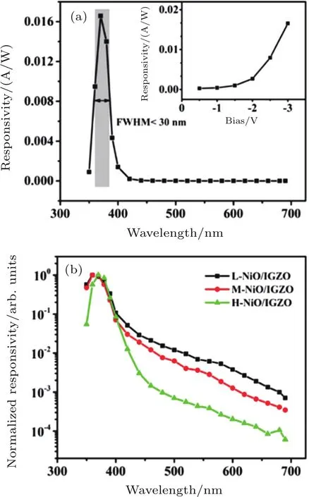
Fig.7.(a)Spectral responsivity of the ITO/H-NiO(high conductivity NiO)/IGZO/ITO photodetector under the bias of?3 V.The inset shows the responsivity as a function of the reverse bias.(b)Normalized spectral responsivities of the ITO/L–NiO(low conductivity NiO)/IGZO/ITO,ITO/M–NiO(medium conductivity NiO)/IGZO/ITO,and ITO/H–NiO/IGZO/ITO photodetector structures at?3-V bias.[138]
Tsai et al.[139]fabricated p-NiO/n-ZnO by RF magnetron sputtering on glass substrate.The current–voltage curve of the heterojunction demonstrated obvious rectifying diode behavior in a dark environment.The lowest leakage current was 7.73×10?8A/cm2for n-ZnO/p-NiO heterojunction diode.In 2017,Patel et al.[140]realized the high transparent selfpowered heterojunction photodetector of the configuration of NiO/ZnO/ITO/polyethylene terephthalate(PET)by using the solid-state sputtering method.This high visible-range transparent(74.8%)photodetector was extremely sensitive to the tiny UV light density.
6.Conclusion and perspectives
This review has introduced ultraviolet photodetectors based on wide bandgap oxide semiconductor films,including ZnO,ZnMgO,Ga2O3,TiO2,and NiO.The growth method of the materials,the classification of the photodetectors,and the development of performance of the devices have been reviewed and summarized.Recent progresses and challenges in this field are systematically discussed.Systematic comparison of photodetector performances based on these devices has been summarized in Table 1.It is clear that these devices will play a significant role in environmental monitoring,medical analysis,defense technology,and fire protection due to their special characteristics of large bandgap,solution processable,low cost,environmentally friendly,etc.Although many important progresses have been achieved on wide bandgap oxide semiconductor films,there is still a lot of work to be done in the field of UV photodetectors based on wide band gap oxide semiconductors,such as p-type doping,the improvement of the materials’quality,the design of the device structure,and so on.
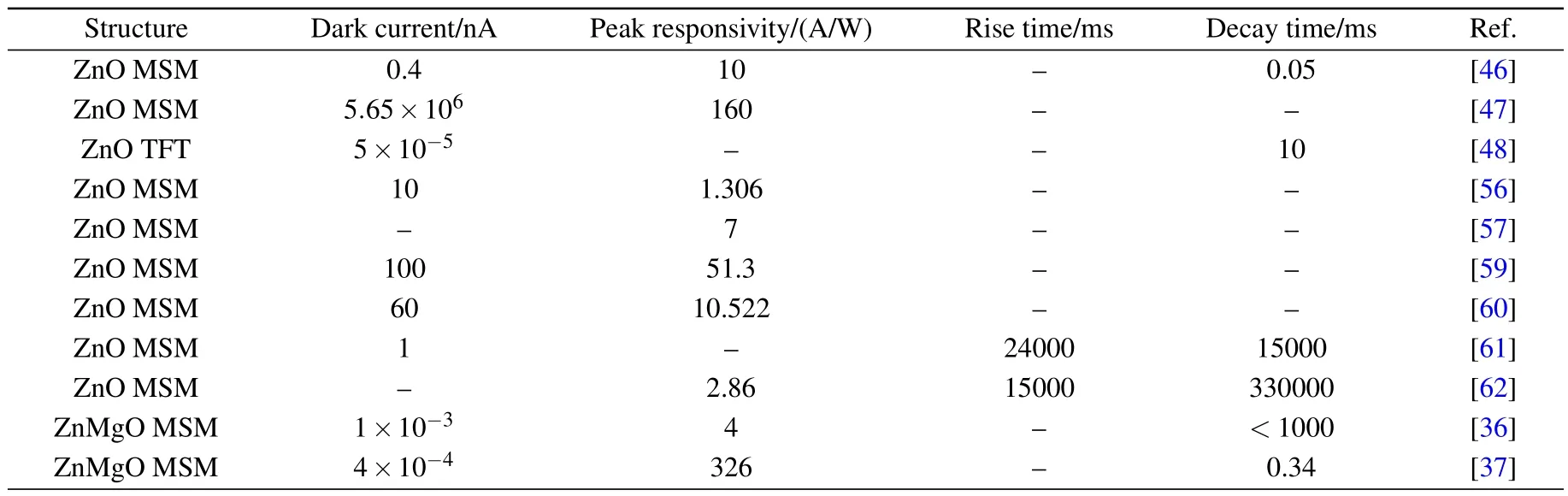
Table 1.Comparison of the photodetector performances for wide bandgap oxide photodetector.
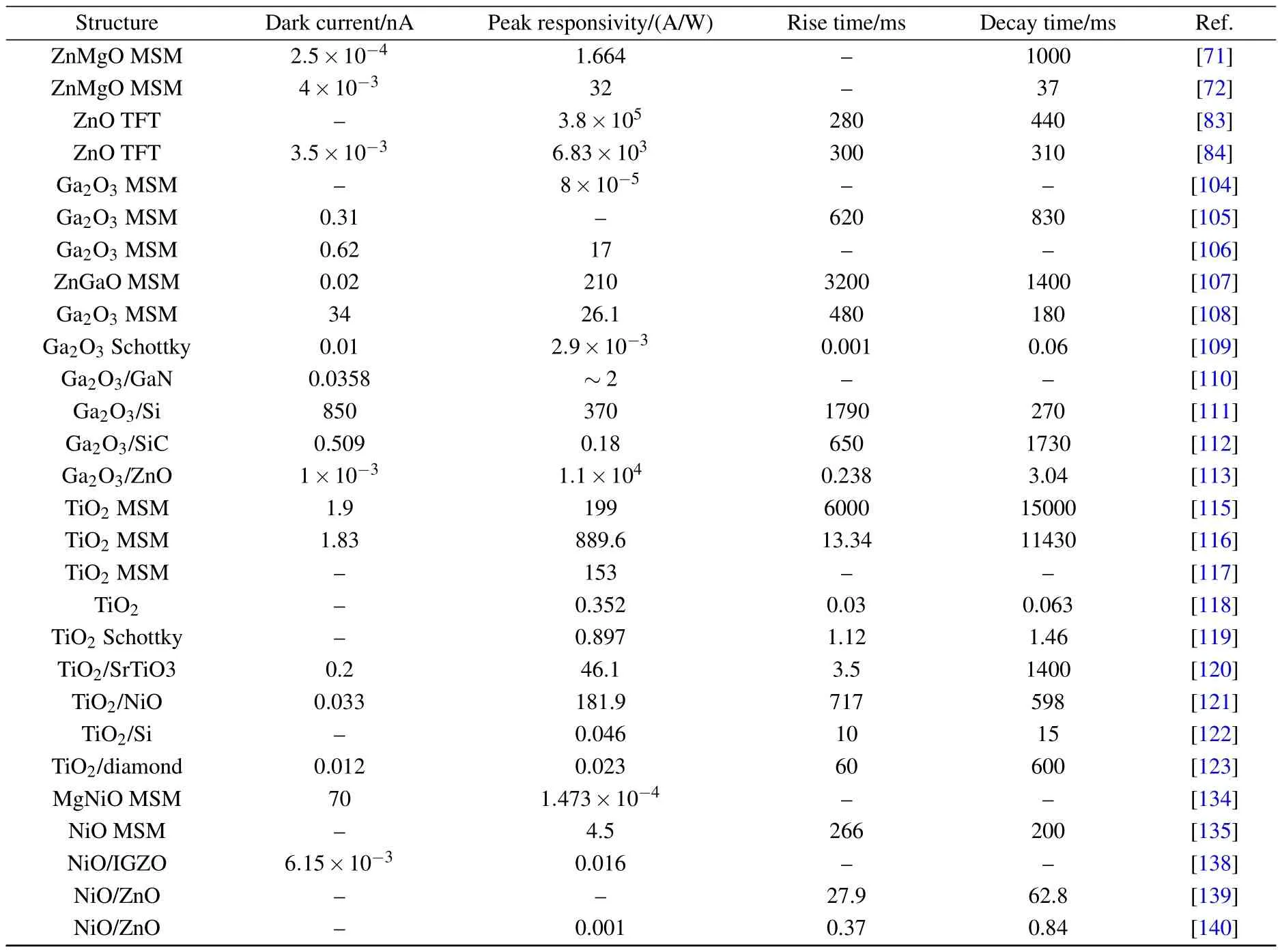
Table 1.(Continued).
[1]Soci C,Zhang A,Xiang B,Dayeh S A,Aplin D P R,Park J,Bao X Y,Lo Y H and Wang D 2007 Nano Lett.7 1003
[2]Aga R S,Jowhar D,Ueda A,Pan Z,Collins W E,Mu R,Singer K D and Shen J 2007 Appl.Phys.Lett.91 232108
[3]Mendoza F,Makarov V,Weiner B R and Morell G 2015 Appl.Phys.Lett.107 201605
[4]Razeghi M and Rogalski A 1996 J.Appl.Phys.79 7433
[5]Müller A,Konstantinidis G, Dragoman M, Neculoiu D, Dinescu A, Androulidaki M, Kayambaki M, Stavrinidis A, Vasilache D, Buiculescu C, Petrini I, Kostopoulos A and Dascalu D 2009 Microelectron.J.40 319
[6]Yang W F,Zhang F,Liu Z G and Wu Z Y 2008 Mater.Sci.Semicond.Process.11 59
[7]Pramanik P,Sen S,Singha C,Roy AS,Das A,Sen S and Bhattacharyya A 2016 J.Appl.Phys.120 144502
[8]Lai Y Y,Lan Y P and Lu T C 2013 Light Sci.Appl.2 e76
[9]Inamdar S I and Rajpure K Y 2014 J.Alloys Compd.595 55
[10]Bai Z M,Yan X Q,Chen X,Zhao K,Lin P and Zhang Y 2014 Prog.Nat.Sci.:Mater.Int.24 1
[11]Liang F X,Zhang D Y,Wang J Z,Kong W Y,Zhang Z X,Wang Y and Luo L B 2016 Opt.Express 24 25922
[12]Vikas L S,Vanaja K A,Subha P P and Jayaraj M K 2016 Sens.Actuat.A:Phys.242 116
[13]Liu K,Sakurai M and Aono M 2010 Sensors 10 8604
[14]Hou Y,Mei Z and Du X 2014 J.Phys.D:Appl.Phys.47 283001
[15]Yang J L,Liu K W and Shen D Z 2017 Chin.Phys.B 26 047308
[16]Zhai T Y,Fang X S,Liao M Y,Xu X J,Zeng H B,Yoshio B D and Golberg D 2009 Sensors 9 6504
[17]Tian W,Lu H and Li L 2015 Nano Res.8 382
[18]Choopun S,Vispute R D,Yang W,Sharma R P,Venkatesan T and Shen H 2002 Appl.Phys.Lett.80 1529
[19]Auret F D,Goodman S A,Hayes M,Legodi M J,van Laarhoven H A and Look D C 2001 Appl.Phys.Lett.79 3074
[20]Ohtomo A,Kawasaki M,Koida T,Masubuchi K,Koinuma H,Sakurai Y,Yoshida Y,Yasuda T and Segawa Y 1998 Appl.Phys.Lett.72 2466
[21]Chen H Y,Liu K W,Hu L F,Al-Ghamdi A A and Fang X S 2015 Mater.Today 18 493
[22]Yang W,Vispute R D,Choopun S,Sharma R P,Venkatesan T and Shen H 2001 Appl.Phys.Lett.78 2787
[23]Xie X,Zhang Z,Li B,Wang S,Jiang M,Shan C,Zhao D,Chen H and Shen D 2014 Opt.Express 22 246
[24]Hou Y N,Mei Z X,Liang H L,Ye D Q,Gu C Z and Du X L 2013 Appl.Phys.Lett.102 153510
[25]Gold A 2010 Appl.Phys.Lett.96 242111
[26]Xie X,Zhang Z,Li B,Wang S and Shen D 2015 Opt.Express 23 32329
[27]Hou Y,Mei Z,Liang H,Ye D,Gu C,Du X and Lu Y 2013 IEEE Trans.Electron.Dev.60 3474
[28]Look D C 2001 Mater.Sci.Eng.B 80 383
[29]Chen H Y,Liu K W,Chen X,Zhang Z Z,Fan M M,Jiang M M,Xie X H,Zhao H F and Shen D Z 2014 J.Mater.Chem.C 2 9689
[30]?zgürüAlivov YI,Liu C,Teke A,Reshchikov MA,Do?an S,Avrutin V,Cho S J and Morkoc?H 2005 J.Appl.Phys.98 041301
[31]Xie X H,Zhang Z Z,Shan C X,Chen H Y and Shen D Z 2012 Appl.Phys.Lett.101 081104
[32]Zheng Q H,Huang F,Ding K,Huang J,Chen D G,Zhan Z B and Lin Z 2011 Appl.Phys.Lett.98 221112
[33]Wang P,Zheng Q H,Tang Q,Yang Y T,Guo L X,Huang F,Song Z J and Zhang Z Y 2014 Opt.Lett.39 375
[34]Kind H,Yan H Q,Messer B,Law M and Yang P D 2002 Adv.Mater.14 158
[35]Chen Q,Ding H,Wu Y,Sui M,Lu W,Wang B,Su W,Cui Z and Chen L 2013 Nanoscale 5 4162
[36]Zhu Y,Liu K,Wang X,Yang J,Chen X,Xie X,Li B and Shen D 2017 J.Mater.Chem.C 5 7598
[37]Chen X,Liu K,Wang X,Li B,Zhang Z,Xie X and Shen D 2017 J.Mater.Chem.C 5 10645
[38]Coppa B J,Davis R F and Nemanich R J 2003 Appl.Phys.Lett.82 400
[39]Azhar E A,Ye W,Helfrecht B,Chen G,Thompson L,Yu H and Dey S 2018 IEEE Trans.Electron.Dev.65 3291
[40]Liu Q,Maogang M,Cook B,Thapa P,Ewing D,Casper M,Stramel A and Wu J 2017 Phys.Status Solidi A 214 1700176
[41]Coppa B J,Fulton C C,Kiesel S M,Davis R F,Pandarinath C,Burnette J E,Nemanich R J and Smith D J 2005 J.Appl.Phys.97 103517
[42]Lee S H,Kim S H and Yu J S 2016 Nanoscale Res.Lett.11 333
[43]Guo F,Yang B,Yuan Y,Xiao Z,Dong Q,Bi Y and Huang J 2012 Nat.Nanotechnol.7 798
[44]Cuong T V,Tien H N,Luan V H,Pham V H,Chung J S,Yoo D H,Hahn S H,Koo K K,Kohl P A,Hur S H and Kim E J 2011 Phys.Status Solidi A 208 943
[45]Ko W,Lee S,Myoung N and Hong J 2016 J.Mater.Chem.C 4 142
[46]Liu M and Kim H K 2004 Appl.Phys.Lett.84 173
[47]Angadi B,Park H C,Choi H W,Choi J W and Choi W K 2007 J.Phys.D:Appl.Phys.40 1422
[48]Reyes P I,Ku C J,Duan Z,Xu Y,Garfunkel E and Lu Y 2012 Appl.Phys.Lett.101 031118
[49]Rostami A,Dolatyari M,Amini E,Rasooli H,Baghban H and Miri S 2013 ChemPhysChem.14 554
[50]Jin Z and Wang J 2014 J.Mater.Chem.C 2 1966
[51]Xu X,Shukla S,Liu Y,Yue B,Bullock J,Su L,Li Y,Javey A,Fang X and Ager J W 2018 Phys.Status Solidi RRL 12 1700381
[52]Li H,Fan C,Wu G,Chen H and Wang M 2010 J.Phys.D:Appl.Phys.43 425101
[53]Sun L,Jiang D,Zhang G,Liu R,Duan Q,Qin J,Liang Q,Gao S,Hou J,Zhao J,Liu W and Shen X 2016 J.Appl.Phys.119 044508
[54]Rajan A,Kaur G,Paliwal A,Yadav H K,Gupta V and Tomar M 2014 J.Phys.D:Appl.Phys.47 425102
[55]Hwang J D,Wang F H,Kung C Y and Chan M C 2015 IEEE Trans.Nanotechnol.14 318
[56]Tian C,Jiang D,Li B,Lin J,Zhao Y,Yuan W,Zhao J,Liang Q,Gao S,Hou J and Qin J 2014 ACS Appl.Mater.Inter.6 2162
[57]Pei J,Jiang D,Zhao M,Duan Q,Liu R,Sun L,Guo Z,Hou J,Qin J,Li B and Zhang G 2016 Appl.Surf.Sci.389 1056
[58]Tong C,Yun J,Kozarsky E and Anderson W A 2013 J.Electron.Mater.42 889
[59]Li G,Song J,Zhang J and Hou X 2014 Solid State Electron.92 47
[60]Li G,Zhang J,Chen G,Ye H,Duan X and Hou X 2016 Solid State Electron.123 33
[61]Sun M W,Xu Z,Yin M,Lin Q F,Lu L F,Xue X Z,Zhu X F,Cui Y X,Fan Z Y,Ding Y L,Tian L,Wang H,Chen X Y and Li D D 2016 Nanoscale 8 8924
[62]Wang X,Liu K,Chen X,Li B,Jiang M,Zhang Z,Zhao H and Shen D 2017 ACS Appl.Mater.Inter.9 5574
[63]Guo Z,Jiang D,Zhao M,Guo F,Pei J,Liu R,Sun L,Hu N and Zhang G 2016 Solid State Electron.124 24
[64]Miao J,Hu W,Jing Y,Luo W,Liao L,Pan A,Wu S,Cheng J,Chen X and Lu W 2015 Small 11 2392
[65]Schoenfeld W V,Wei M,Boutwell R C and Liu H 2014 Proc.SPIE 8987 89871
[66]Jiang D Y,Shan C X,Zhang J Y,Lu Y M,Yao B,Zhao D X,Zhang Z Z,Shen D Z and Yang C L 2009 J.Phys.D:Appl.Phys.42 025106
[67]Liu K W,Shen D Z,Shan C X,Zhang J Y,Jiang D Y,Zhao Y M,Yao B and Zhao D X 2008 J.Phys.D:Appl.Phys.41 125104
[68]Shukla G 2009 IEEE Photon.Technol.Lett.21 887
[69]Boutwell R C,Wei M and Schoenfeld W V 2013 Appl.Phys.Lett.103 031114
[70]Zheng Q,Huang F,Huang J,Hu Q,Chen D and Ding K 2013 CrystEngComm 15 2709
[71]Fan M M,Liu K W,Zhang Z Z,Li B H,Chen X,Zhao D X,Shan C X and Shen D Z 2014 Appl.Phys.Lett.105 011117
[72]Fan M M,Liu K W,Chen X,Wang X,Zhang Z Z,Li B H and Shen D Z 2015 ACS Appl.Mater.Inter.7 20600
[73]Han S,Liu S M,Lu Y M,Cao P J,Liu W J,Zeng Y X,Jia F,Liu X K and Zhu D L 2017 J.Alloys Compd.694 168
[74]Han S,Liu S M,Liu W J,Cao P J,Lu Y M,Zeng Y X,Jia F,Liu X K,Zhu D L and Su S C 2016 J.Phys.Chem.C 120 12568
[75]Han S,Ji X H,An Q L,Lu Y M,Cao P J,Liu W J,Zeng Y X,Jia F,Liu X K and Zhu D L 2017 J.Mater.Chem.C 5 11472
[76]Luo W,Weng Q,Long M,Wang P,Gong F,Fang H,Luo M,Wang W,Wang Z,Zheng D,Hu W,Chen X and Lu W 2018 Nano.Lett.18 5439
[77]Zheng D,Fang H,Wang P,Luo W,Gong F,Ho J,Chen X,Lu W,Liao L,Jianlu Wang J and Hu W 2016 Adv.Funct.Mater.26 7690
[78]Zheng D,Wang J,Hu W,Liao L,Fang H,Guo N,Wang P,Gong F,Wang X,Fan Z,Wu X,Meng X,Chen X and Lu W 2016 Nano Lett.16 2548
[79]Chen Y,Wang X,Wang P,Huang H,Wu G,Tian B,Hong Z,Wang Y,Sun S,Shen H,Wang J,Hu W,Sun J,Meng X and Chu J 2016 ACS Appl.Mater.Inter.8 32083
[80]Wang X,Wang P,Wang J,Hu W,Zhou X,Guo N,Huang H,Sun S,Shen H,Lin T,Tang M,Liao L,Jiang A,Sun J,Meng X,Chen X,Lu W and Chu J 2015 Adv.Mater.27 6575
[81]Wang J L,Fang H H,Wang X D,Chen X S,Lu W and Hu W D 2017 Small 13 1700894
[82]Tian H,Wang X,Zhu Y,Liao L,Wang X,Wang J and Hu W 2017 Appl.Phys.Lett.110 043505
[83]Wang P,Wang Y,Ye L,Wu M,Xie R,Wang X,Chen X,Fan Z,Wang J and Hu W 2018 Small 14 1800492
[84]Wang Y,Wang P,Zhu Y,Gao J,Gong F,Li Q,Xie R,Wu F,Wang D,Yang J,Fan Z,Wang X and Hu W 2019 Appl.Phys.Lett.114 011103
[85]Wang J and Hu W 2017 Chin.Phys.B 26 037106
[86]Xu M,Ge L,Han M,Huang J,Xu H and Yang Z 2019 Chin.Phys.B 28 028502
[87]Suzuki R,Nakagomi S and Kokubun Y 2011 Appl.Phys.Lett.98 131114
[88]Ji Z G,Du J,Fan J and Wang W 2006 Opt.Mater.28 415
[89]Rafique S,Han L and Zhao HP2017Phys.Status Solidi A2141700063
[90]Ghose S,Rahman S,Hong L,Rojas-Ramirez J S,Jin H,Park K,Klie R and Droopad R 2017 J.Appl.Phys.122 095302
[91]Orita M,Ohta H,Hirano M and Hosono H 2000 Appl.Phys.Lett.77 4166
[92]Oshima T,Okuno T and Fujita S 2007 Jpn.J.Appl.Phys.46 7217
[93]Weng W Y,Hsueh T J,Chang S J,Huang G J and Hsueh H T 2011 IEEE Sens.J.11 999
[94]Wei T C,Tsai D S,Ravadgar P,Ke J J,Tsai M L,Lien D H,Huang C Y,Horng R H and He J H 2014 IEEE J.Sel.Top.Quantum Electron.20 3802006
[95]Yu F P,Ou S L and Wuu D S 2015 Opt.Mater.Express 5 1240
[96]Wu Z H,Qian L X,Sheng T,Zhang Y Y and Liu X Z 2016 IEEE Int.Conf.Electron.Devices Solid-State Circuits 82
[97]Liu X Z,Guo P,Sheng T,Qian L X,Zhang W L and Li Y R 2016 Opt.Mater.51 203
[98]Cui S J,Mei Z X,Zhang Y H,Liang H L and Du X L 2017 Adv.Opt.Mater.5 1700454
[99]Qian Y P,Guo D Y,Chu X L,Shi H Z,Zhu W K,Wang K,Huang X K,Wang H,Wang S L,Li P G,Zhang X H and Tang W H 2017 Mater.Lett.209 558
[100]Li P G,Shi H Z,Chen K,Guo D Y,Cui W,Zhi Y S,Wang S L,Wu Z P,Chen Z W and Tang W H 2017 J.Mater.Chem.C 5 10562
[101]Wu Z P,Jiao L,Wang X L,Guo D Y,Li W H,Li L H,Huang F and Tang W H 2017 J.Mater.Chem.C 5 8688
[102]An Y H,Zhi Y S,Wu Z P,Cui W,Zhao X L,Guo D Y,Li P G and Tang W H 2016 Appl.Phys.A 122 1036
[103]Nakagomi S,Momo T,Takahashi S and Kokubun Y 2013 Appl.Phys.Lett.103 072105
[104]Kokubun Y,Miura K,Endo F and Nakagomi S 2007 Appl.Phys.Lett.90 031912
[105]Guo D Y,Wu Z P,An Y H,Guo X C,Chu X L,Sun C L,Li L H,Li P G and Tang W H 2014 Appl.Phys.Lett.105 023507
[106]Hu G C,Shan C X,Zhang N,Jiang M M,Wang S P and Shen D Z 2015 Opt.Express 23 13554
[107]Alema F,Hertog B,Ledyaev O,Volovik D,Thoma G,Miller R,Osinsky A,Mukhopadhyay P,Bakhshi S,Ali H and Schoenfeld W V 2017 Phys.Status Solidi A 214 1600688
[108]Zhang D,Zheng W,Lin R C,Li T T,Zhang Z J and Huang F 2018 J.Alloys Compd.735 150
[109]Chen X,Liu K W,Zhang Z Z,Wang C R,Li B H,Zhao H F,Zhao D X and Shen D Z 2016 ACS Appl.Mater.Inter.8 4185
[110]Weng W Y,Hsueh T J,Chang S J,Huang G J and Hsueh H T 2011 IEEE.Sens.J.11 1491
[111]Guo X C,Hao N H,Guo D Y,Wu Z P,An Y H,Chu X L,Li L H,Li P G,Lei M and Tang W H 2016 J.Alloys Compd.660 136
[112]Qu Y Y,Wu Z P,Ai M L,Guo D Y,An Y H,Yang H J,Li L H and Tang W H 2016 J.Alloys Compd.680 247
[113]Chen X H,Xu Y,Zhou D,Yang S,Ren F F,Lu H,Tang K,Gu S L,Zhang R,Zheng Y D and Ye J D 2017 ACS Appl.Mater.Inter.9 36997
[114]Zou J,Zhang Q,Huang K and Marzari N 2010 J.Phys.Chem.C 114 10725
[115]Xue H L,Kong X Z,Liu Z R,Liu C X,Zhou J R and Chen W Y 2007 Appl.Phys.Lett.90 201118
[116]Kong X Z,Liu C X,Dong W,Zhang X D,Tao C,Shen L,Zhou J R,Fei Y F and Ruan S P 2009 Appl.Phys.Lett.94 123502
[117]Shih W S,Young S J,Ji L W,Water W,Meen T H and Shiu 2011 IEEE Sens.J.11 3031
[118]Akbari M K,Hai Z Y,Depuydt S,Kats E,Hu J and Zhuiykov S 2017 IEEE.Trans.Nanotechnol.16 880
[119]Patel D B,Chauhan K R,Park W H,Kim H S,Kim J and Yun J H 2017 Mat.Sci.Semicon.Proc.61 45
[120]Zhang M,Zhang H F,Lv K B,Chen W Y,Zhou J R,Shen L and Ruan S P 2012 Opt.Express 20 5936
[121]Zhang D Z,Liu C Y,Xu R L,Yin B,Chen Y,Zhang X D,Gao F L and Ruan S P 2017 Nanotechnology 28 365505
[122]Sun L,Wang C R,Ji T,Wang J L,Yi G C and Chen X S 2017 RSC Adv.7 51744
[123]Liu Z C,Ao J P,Li F N,Wang W,Wang J J,Zhang J W and Wang H X 2017 Mater.Lett.188 52
[124]Hakim A,Hossain J and Khan K 2009 Renew.Energ.34 2625
[125]Al-Ghamdi A A,Abdel-wahab M S,Farghali A A and Hasan P M Z 2016 Mater.Res.Bull.75 71
[126]Ahmed A A,Afzal N,Devarajan M and Subramani S 2016 Mater.Res.Express 3 116405
[127]Caruge J M,Halpert J E,Wood V,Bulovic V and Bawendi M G 2008 Nat.Photon.2 247
[128]Waser R and Aono M 2007 Nat.Mater.6 833
[129]Gibson E A,Smeigh A L,Pleux L L,Fortage J,Boschloo G,Blart E,Pellegrin Y,Odobel F,Hagfeldt A and Hammarstrom L 2009 Angew.Chem.Int.Ed.121 4466
[130]Mallows J,Planells M,Thakare V,Bhosale R,Ogale S and Robertson N 2015 ACS Appl.Mater.Inter.7 27597
[131]Park N,Sun K,Sun Z L,Jing Y and Wang D L 2013 J.Mater.Chem.C.1 7333
[132]Kim D Y,Ryu J,Manders J,Lee J and So F 2014 ACS Appl.Mater.Inter.6 1370
[133]Kim H,Kumar M D,Patel M and Kim J 2016 Mater.Res.Bull.83 35
[134]Zhao Y M,Zhang J Y,Jiang D Y,Shan C X,Zhang Z Z,Yao B,Zhao D X and Shen D Z 2009 J.Phys.D:Appl.Phys.42 092007
[135]Ahmed A A,Devarajan M and Afzal N 2017 Sens.Actuat.A:Phys.262 78
[136]Choi J M and Im S 2005 Appl.Surf.Sci.244 435
[137]Zhang D Y,Nozaki S J and Uchida K 2014 J.Vac.Sci.Technol.B 32 031202
[138]Li H K,Chen T P,Hu S G,Li X D,Liu Y,Lee P S,Wang X P,Li H Y and Lo G Q 2015 Opt.Express 23 27683
[139]Tsai S Y,Hon M H and Lu Y M 2011 Mater.Sci.Forum 687 711
[140]Patel M and Kim J 2017 J.Alloys Compd.729 796
猜你喜歡
小主人報(bào)(2022年2期)2022-01-19 11:46:16
Chinese Physics B(2021年7期)2021-07-30 07:38:52
數(shù)學(xué)小靈通·3-4年級(jí)(2021年5期)2021-07-16 07:46:22
小學(xué)生學(xué)習(xí)指導(dǎo)(中年級(jí))(2021年4期)2021-04-27 10:15:00
數(shù)學(xué)小靈通·3-4年級(jí)(2020年12期)2021-01-14 00:58:44
小學(xué)生學(xué)習(xí)指導(dǎo)(中年級(jí))(2020年12期)2021-01-08 02:50:08
數(shù)學(xué)小靈通·3-4年級(jí)(2017年12期)2018-01-23 03:38:05
神州·下旬刊(2017年6期)2017-10-28 01:13:14
作文評(píng)點(diǎn)報(bào)·低幼版(2017年1期)2017-03-10 20:44:09
藝術(shù)評(píng)論(2016年10期)2016-11-28 19:43:16

- Chinese Physics B的其它文章
- Effect of carrier mobility on performance of perovskite solar cells?
- Plasma electrolytic liquefaction of sawdust?
- Insight into band alignment of Zn(O,S)/CZTSe solar cell by simulation?
- Effect of terahertz pulse on gene expression in human eye cells?
- A primary model of decoherence in neuronal microtubules based on the interaction Hamiltonian between microtubules and plasmon in the neurons
- Effect of temperature on photoresponse properties of solar-blind Schottky barrier diode photodetector based on single crystal Ga2O3?