
Dynamic modeling of total ionizing dose-induced threshold voltage shifts in MOS devices
2023-02-20 13:16:42GuangbaoLu陸廣寶JunLiu劉俊ChuanguoZhang張傳國(guó)YangGao高揚(yáng)andYonggangLi李永鋼
Chinese Physics B 2023年1期
Guangbao Lu(陸廣寶), Jun Liu(劉俊), Chuanguo Zhang(張傳國(guó)),Yang Gao(高揚(yáng)),2, and Yonggang Li(李永鋼),2,?
1Key Laboratory of Materials Physics,Institute of Solid State Physics,HFIPS,Chinese Academy of Sciences,Hefei 230031,China
2University of Science and Technology of China,Hefei 230026,China
Keywords: dynamic modeling,total ionizing dose,threshold voltage shifts,radiation-hardening
1. Introduction
Silicon-based semiconductor devices are widely-served in the extreme irradiation environments of the aviation and nuclear industries. Irradiation of high-energy rays is one of the main reasons for metal–oxide–semiconductor (MOS) device performance degradation/failure.[1,2]The irradiation effects of MOS devices are mainly divided into displacement and ionizing damage.[3]In particular, ionizing damage is caused by electron excitation to induce electron–hole (e-h)pairs when high-energy particles (such as photons or electrons) pass through the materials. There are two basic effects of ionizing damage, that is, the total ionizing dose(TID) and single event effects, caused by the cumulative effect of high-energy particles[4]and the transient effect of a single high-energy particle,[5]respectively. The TID effect is the main cause of ionizing damage to MOS devices, such as low threshold voltage, low channel mobility, high leakage current, high on-resistance, low breakdown voltage, and electroluminescence.[6–9]Among them, the threshold voltage shift(ΔVth)can cause the permanent failure of devices,which is a major unresolved issue that is sensitive to TID.[10]
The failure of the communication satellite Telstar I in 1963 prompted researchers to study the effects of ionizing radiation.[11]In 1964,Hughes and Giroux conducted the first experimental study on the degradation of MOS devices by the TID effects. They demonstrated significant sensitivity to ionizing radiation in both n-and p-channel transistors.[12]Subsequently, Hugheset al. discovered that the charges generated within the oxide layer rather than on the oxide surface cause the TID effects.[13]In the following decades,researchers studied the electrical properties of different MOS devices like transistors and capacitors under the irradiation of different sources of60Coγ-rays,x-rays and high-energy electrons.[14–16]These experiments confirmed that the key mechanism of the TID effects is the accumulation of positive charges in the oxide layer of MOS devices. However, besides the expensive irradiation testing cost,[17]ΔVthinduced by TID is a multiscale dynamic process from e-h pairs generation to accumulation of charged defects. Whereas, in experiments, it is hard to trace the multiscale dynamic behaviors of mobile particles and defects and distinguish their distributions during irradiation.[18]Therefore,it requires an alternative approach based on theoretical simulation/modeling.
The traditional analytical models are commonly used to study TID by solving the rate equations of oxide charged defects (Not) and interface charged defects (Nit).[19]It is much simple by only considering the two dominant processes including the capture of irradiation-induced holes by oxygen vacancies and the reactions of interface defects with hydrogen molecules(H2). The model fails to take into account the complete interactions,the influence of different irradiation conditions,and the detailed distributions of defects/electric field. In the past decades,the dynamic modeling of the TID effects has also been developed from the original one-dimensional (1D)theoretical model of the oxide layer to the commercial threedimensional(3D)simulation software of devices.[20,21]In addition, the influences of the H2concentration and dose rate on the TID effects were studied in different semiconductor devices.[22,23]In 1988,Srouret al.developed a physical model to study the TID process,and attributed it to four steps,that is,e-h pair generation,free carrier transport,bulk charged defect buildup,and interface charged defect formation.[24]Recently,based on Srour’s model, Esqueda established a 1D analytical model for the SiO2layer to further describe the damage process quantitatively, which is validated by experiments.[25]He provided a comprehensive study of the physical mechanisms contributing to the buildup of bulk and interface charged defects in advanced CMOS technologies. Only two species of defects are considered in his model due to an insufficient understanding of the composition of the oxide layer.More defect species with various configurations and reactions among them need to be clarified and taken into account.[26]Rowseyet al.proposed a 1D quantitative model to accurately describe the dynamic behaviors of defects in the oxide layer, with more realistic defect reactions and parameters,[27]especially for H2and hydrogenated defects acquired by the first-principles calculations.[28]This research provided new insights into the enhanced low-dose-rate sensitivity (ELDRS) in the isolation oxides prevalent in many bipolar devices. Till now, ΔVthof MOS devices after irradiation is mainly attributed to the accumulation of oxide charged defects in the oxide layer,through the mechanisms of holes capture or electrons releasing caused by TID-induced e-h pairs generation. However, there are still challenges in fully understanding the mechanism of TIDinduced ΔVth. Especially, it is needed to more strictly clarify which defect affects the threshold voltage most and through which mechanism. It is also necessary to quantitatively analyze the influence of different sample/service conditions on the TID effects,and figure out the key factors for the design of high radiation-hardened devices.
In this paper, we adopted new reaction mechanisms and parameters mainly from Rowsey’s model,[27]and developed a dynamic model to accurately describe the evolution and distribution of mobile particles and defects in MOS devices by the TID effects. The effects of oxygen vacancy defects and interfacial electric field on the threshold voltage were thus analyzed systematically. This work provides a theoretical guidance for the radiation-hardening-by-design (RHBD) techniques of semiconductor devices.
2. Theoretical model
A 1D dynamic model of mobile particles and defects in the oxide (SiO2) layer is developed to systematically study the TID effects of MOS devices underγ-ray irradiation. The schematic diagram of the 1D SiO2layer of typical MOS devices is shown in Fig. 1. The model can be summarized as follows. First,the initial distributions of defects can be determined by electron paramagnetic resonance measurements.[29]The reaction events and rate coefficients between mobile particles and defects are given by the density functional theory(DFT) calculations.[28]Then, with this information, the continuity equations of mobile particles and defects can be described based on the rate theory. Finally, the finite difference method and the sub-cycle algorithm are employed to solve the stiff ordinary differential equations (ODEs) efficiently. The evolution and distribution of mobile particles and charged defects can thus be obtained by this model. The whole dynamic model framework is shown in Fig.2.
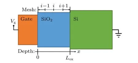
Fig.1.Schematic diagram of the 1D SiO2 layer of typical MOS devices with the boundary conditions of the metal gate and Si substrate on the left and right sides,respectively.
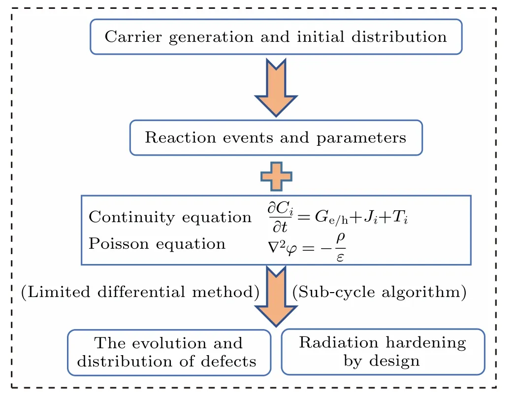
Fig.2. Dynamical model framework for particles and defects.
2.1. Continuity equations
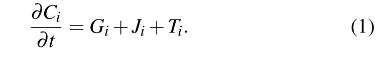
The dynamic model of mobile particles and defects is based on numerically solving a set of coupled continuity equations,as given by HereCirepresents the concentration of particleiat a certain position at a certain time.Gi,TiandJirepresent the generation(only for electron/hole),reaction(with other defects)and drift-diffusion (only for mobile particles) rates of particlei,respectively.
According to experimental findings, the following reasonable approximations are applied here:

2) Before irradiation, the initial defect concentration in the oxide layer seriously depends on the fabricating process of MOS devices,which is uniform distribution approximately.The concentration values[29,30]under typical conditions used in the simulation are given in Table 1.
3) Only the de-passivated reaction (H++Si–H→Nit+H2) with the thermal activation energy of 0.2 eV is involved,while the passivated reaction with the energy of 1.3 eV cannot occur at the temperature studied here.[31]
4) Since the mobility of charged defects is much lower than that of carriers under electric field, they are reasonably treated as immobile. In addition,the reactions of electron capture and emission by charged defects occur locally. Therefore,the migration of the charged defect has nearly no effect on the simulation results.
2.1.1. Generation of electron–hole pairs
Asγ-rays pass through the oxide layer,high-energy photons transfer energy to electrons to excite uniform e-h pairs through direct or indirect ionizing processes. The generation rate of e-h pairs induced by the ionizing irradiation is given as follows:[32]

whereG0represents the density of e-h pairs per unit ionizing dose,Yis the survival rate of the e-h pairs after the initial recombination, which is set to be 0.01 for SiO2underγ-ray irradiation,[18]andRis the dose rate(rad/s).
2.1.2. Reactions of mobile particles with defects
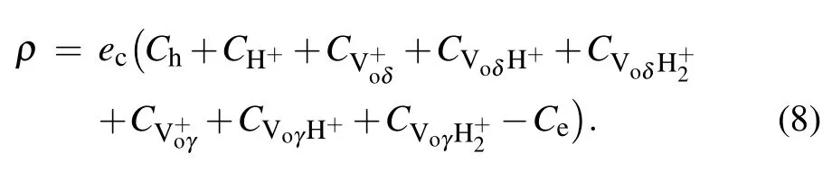
The commonly oxidation process will produce 1014–1018cm-3oxygen vacancy (Voγand Voδ) and hydrogenated oxygen vacancy(VoδH, VoδH2, VoγH and VoγH2) defects in the oxide layer,[33]whose concentrations are given in Table 1.H2is also introduced during the oxidation process, typically with a concentration of 1014–1020cm-3.[26]Oxygen vacancy can trap a hole to generate a positively charged defect that can crack H2to release a H+or serve as a recombination center.Hydrogenated oxygen vacancy also can trap a hole to generate a positively charged defect that can directly release a H+/H2or serve as a recombination center.[25,29,30]The rate coefficientsαandβare formulated based on the reaction barriers obtained by DFT.The specific reaction events and rate coefficients are listed in Table 1. The reaction rates of mobile particles with defects are determined by the rate theory, which is proportional to the reactant concentrations. Comprehensively considering all reaction events (Table 1), the net generation rate of particleiis given by[29]
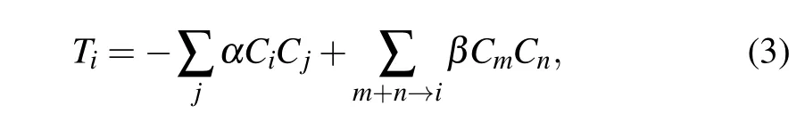
wherej,mandnare termed as the other reactants,andαandβrepresent the forward and reverse reaction rate coefficients,respectively.
An important parameter is the density ofNot, in units of[cm-2], which can be determined by integrating the distribution of each oxide charged defect as[25]
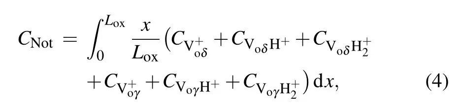
whereLoxis the thickness of the oxide layer, andxrefers to the distance from the gate.
In the high-temperature environment of hundreds of degrees Celsius during the oxidation process, the silicon dangling bonds at the Si/SiO2interface are passivated to form Si–H bonds. During ionizing irradiation, the generated H+will react with Si–H bonds to form H2and the interface charged defect Si–(Nit),[31]that is,H++Si–H→Nit+H2. The corresponding rate equation ofNitformation can be given by[18]
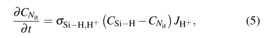
where,σSi-H,H+is the capture cross-section,CSi-HandCNitare the surface densities of the interfacial Si–H bonds and charged Si–bonds,respectively.
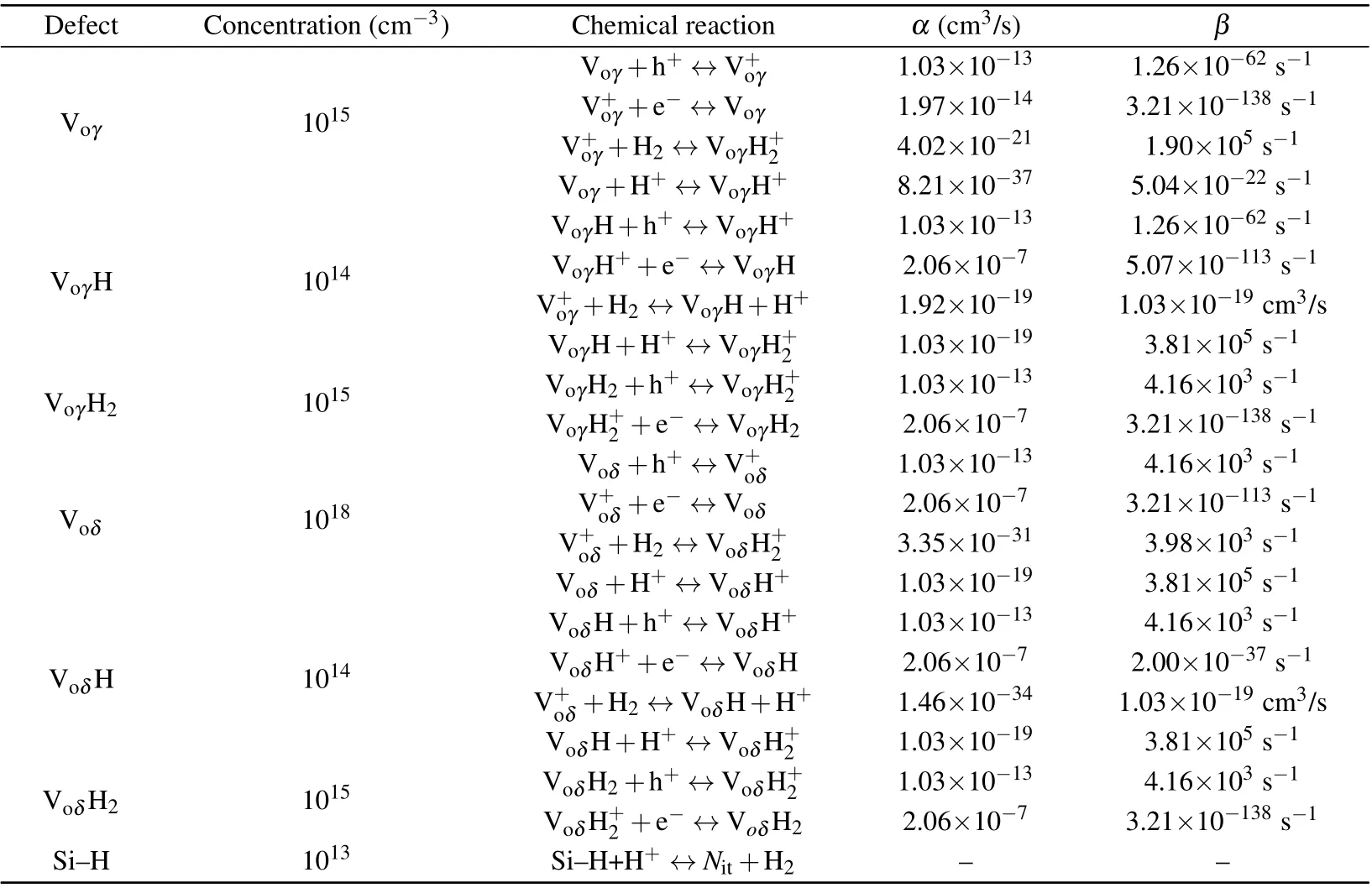
Table 1. Reaction events and rate coefficients.
2.1.3. Drift-diffusion of mobile particles
Mobile particles can diffuse driven by the gradient of concentration, and mobile charged particles can drift under the electric field in the SiO2layer. The drift-diffusion equation is given as follows:[34]
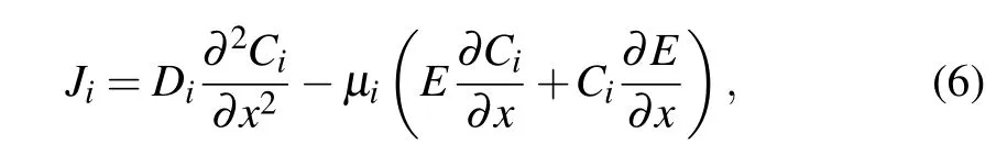
whereμirepresents the mobility of mobile charged particles,Di=μikBT/qrepresents the diffusion coefficients of mobile particles,andErepresents the electric field along the grid direction.

where
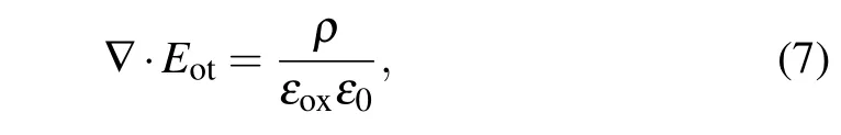
Here,ρis the total charge density in the oxide layer,ecis the elementary charge,εoxis the relative permittivity of SiO2,andε0is the vacuum permittivity.
In addition,the constant electric field induced by the accumulation of interface charged defects in the oxide layer can be given by taking the gate–SiO2–Si system as a parallel plate capacitor as[35,36]
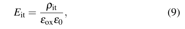
whereρit=eCNitrepresents the charge density at the interface.
2.2. Numerical method
The finite difference method with a uniform spatial grid is adopted for solving the partial differential equations (PDEs).Here thelsodasolver of theCversion is employed to solve the corresponding ODEs.
2.2.1. Boundary conditions.
As shown in Fig.1,the boundary conditions of the oxide layer in solving the ODEs are set as follows:
1)For the mobile particles except for protons,the absorption boundary conditions are adopted at the interfaces of both gate/SiO2and Si/SiO2as
2) For protons, the absorption boundary conditions are also adopted at the interface of gate/SiO2as
and the third boundary condition on the interface of Si/SiO2is typically set as
to consider the reaction with the interface defects, wherek=10-11is the reaction coefficient of H+and Si–H.
2.2.2. Sub-cycle algorithm
The continuity equation includes the evolution of both mobile particles and defects, with the former rates generally much higher than the latter. It makes the above ODEs become typical stiff equations,leading to very low solution efficiency.Thus,we introduced a sub-cycle algorithm[37]to accelerate the solution of these ODEs. The basic idea of the sub-cycle algorithm is to select different time steps at different time scales of particles and defects in solving ODEs.Time nodes are divided into two groups. One is the main cycle groupTicorresponding to defect dynamics,which represents the global time step.The other is the sub-cycle groupticorresponding to particle dynamics, which represents the local time step that is much smaller than the global time step.
In the numerical solution, the time nodes are circularly advanced. First,the continuity equation of mobile particles is solved and the local time nodes,t1,t2,t3,...,are iterated successively, until the global time nodeT1is reached. Secondly,the continuity equation of defects is iterated to the global time nodeT1to complete the iteration. Then, the same iterations are repeated until the final time node is reached.
3. Results
In this section,we firstly verified our model according to the experimental data of an NPN-type MOS capacitor irradiated byγ-rays.[25]Secondly,we gave the evolution and distribution of defects and electric field in the SiO2layer to study the TID-induced threshold voltage shifts. Finally, we studied several hardened methods for the threshold voltage shifts. The physical parameters involved in the model are given in Table 2.
Table 2. Physical parameters used in simulations.
3.1. Validation and verification
The simulated densities of oxide(Not)and interface(Nit)charged defects are compared with the experimental ones[25]to verify our model. Figure 3 shows the time evolution of the densities ofNotandNit, under the time of 1.5×10⁴s with the dose rate of 20 rad/s at 300 K.The capacitance–gate voltage curves of the irradiated devices under three different TIDs were measured to determine the average densities ofNotandNit. Typically,bothNotandNitincrease gradually with irradiation time and tend to saturation. The simulation results are almost consistent with the experimental ones.
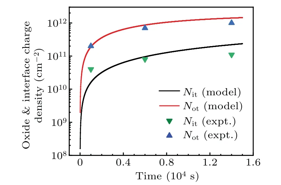
Fig.3. Comparison of the evolution of Not and Nit with the experiment for the MOS capacitor with a 200 nm SiO2 layer under 5 V bias.
In addition,Notis higher thanNit,which is mainly determined by the initial densities of oxygen vacancies and Si–H bonds. Thus,our model should be reasonable enough for simulating the TID effects.
3.2. Distribution and evolution of charged particles and electric field
Compared toNit,Notplays a dominant role in TIDinduced ΔVth.[35]Therefore, it is necessary to study the key factors of the oxide charged defects for the TID effects, such as the composition,distribution and evolution. Here the distributions of oxide charged defects,carriers,charge and electric field are simulated under the TID of 10 krad with the dose rate of 10 rad/s at 300 K. The distribution of carriers induced by irradiation determines the distributions of oxide charged defects. The carriers and charged defects will cause the formation of the built-in electric field that changes the distribution of the total electric field,which will in turn affect the distribution of carriers and charged defects.
Figure 4(a) shows the distributions of different oxide charged defects. Although the initial density of Voδis the highest in the oxide layer,and VoγH+are the main components of the oxide charged defects. It is because the capture probability (1.97×10⁻¹⁴) offor electrons (+ e→Voγ) is comparable to that (1.03×10⁻¹³) of Voγfor holes(Voγ+h→)and lower than the electron capture probability (2.06×10⁻⁷) of other charged defects (V+oδ+e→Voδ).Thus, it is easier for Voγto formthan Voδto form.Also shown in Fig.4(a),with the increasing distance from the gate,the densities of charged oxygen vacancies(and)and charged singly-hydrogenated oxygen vacancies (VoγH+and VoδH+)slowly increase in the oxide layer but decrease at the boundary. It is mainly because the changes in their densities are determined by the distribution of hole density through capturing holes that are low at the boundaries, as shown in Fig.4(b). With the positive electric field,the density of holes and electrons becomes higher and lower as the distance from the gate increases, respectively. But because they flow out at the boundaries, the densities of holes and electrons decrease rapidly at the Si/SiO2and gate/SiO2interfaces, respectively.Due to the competition between the electric field drive and the boundary absorption, the positions with the highest hole and electron densities are about 30 nm from the Si/SiO2and gate/SiO2boundaries, respectively. Therefore, the accumulation distribution of holes determines the distributions of,VoγH+,and VoδH+, also with the peak at 30 nm from the Si/SiO2interface. Although the proportion of charged doubly-hydrogenated vacancies (and) is not high, they promote the formation of major charged defects(and VoγH+). With the increasing distance from the gate,their densities first increase and then decrease, and rise again at the Si/SiO2boundary. From 0 to 30 nm,the reaction of the initial defects capturing holes is dominant,and their densities are affected by the holes.From 30 nm to 200 nm,the releasing proton reaction of the charged defects is dominant, and their densities are affected by, VoγH+,and VoδH+. The spatial distributions of charged defects and carriers contribute to the spatial charge distribution, as shown in Fig. 4(c). The trend of its distribution is determined by all the free charges mainly contributed byand VoγH+. The charge density near the Si/SiO2interface is higher than that in the oxide layer,and the peak is also located at 30 nm from the Si/SiO2interface. The spatial charges further induce the built-in electric field, as shown in Fig. 4(d). The initial electric field is uniform,while the total and build-in electric fields increase with the position after irradiation.The built-in electric field is negative and positive near the gate/SiO2and Si/SiO2interfaces,respectively. The reversal point locates at 120 nm,which means that the electric field created by the spatial charges is negative in the 0–120 nm range and positive in the range of 120–200 nm.This is related to the position of the peak of the spatial charges.dominates the distribution of the space charges,then the spatial charges determine the distribution of the builtin electric field. And the electric field at the Si/SiO2interface ultimately affects the change of the threshold voltage. The positive built-in electric field at the Si/SiO2interface has an enhancement effect on the initial electric field, as shown in Fig. 4(d). It will increase the carrier (electron) density in the channel, and the required conduction voltage (that is, the device threshold voltage)is reduced accordingly.
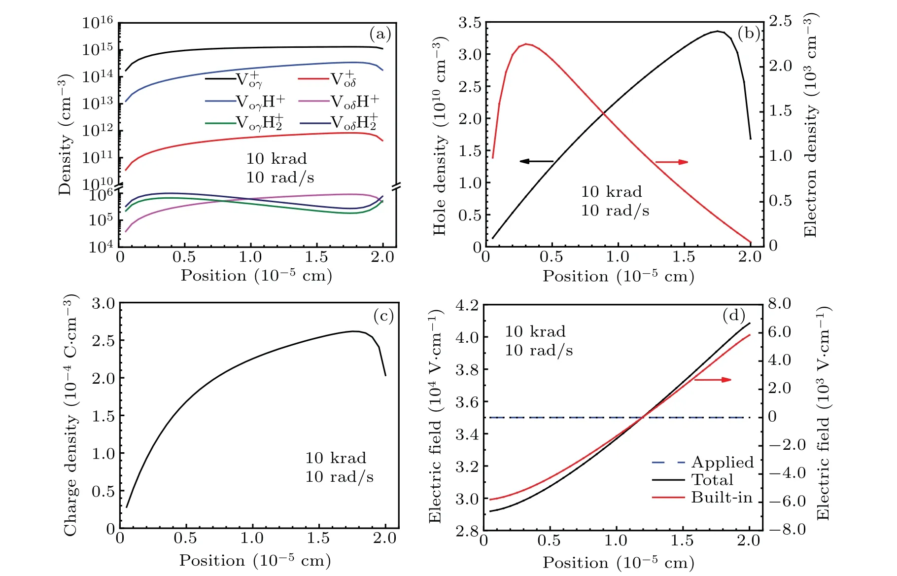
Fig.4. Distributions of(a)different oxide charged defects,(b)carriers,(c)total charge density and(d)electric fields,under the TID of 10 krad with the dose rate of 10 rad/s at 300 K.
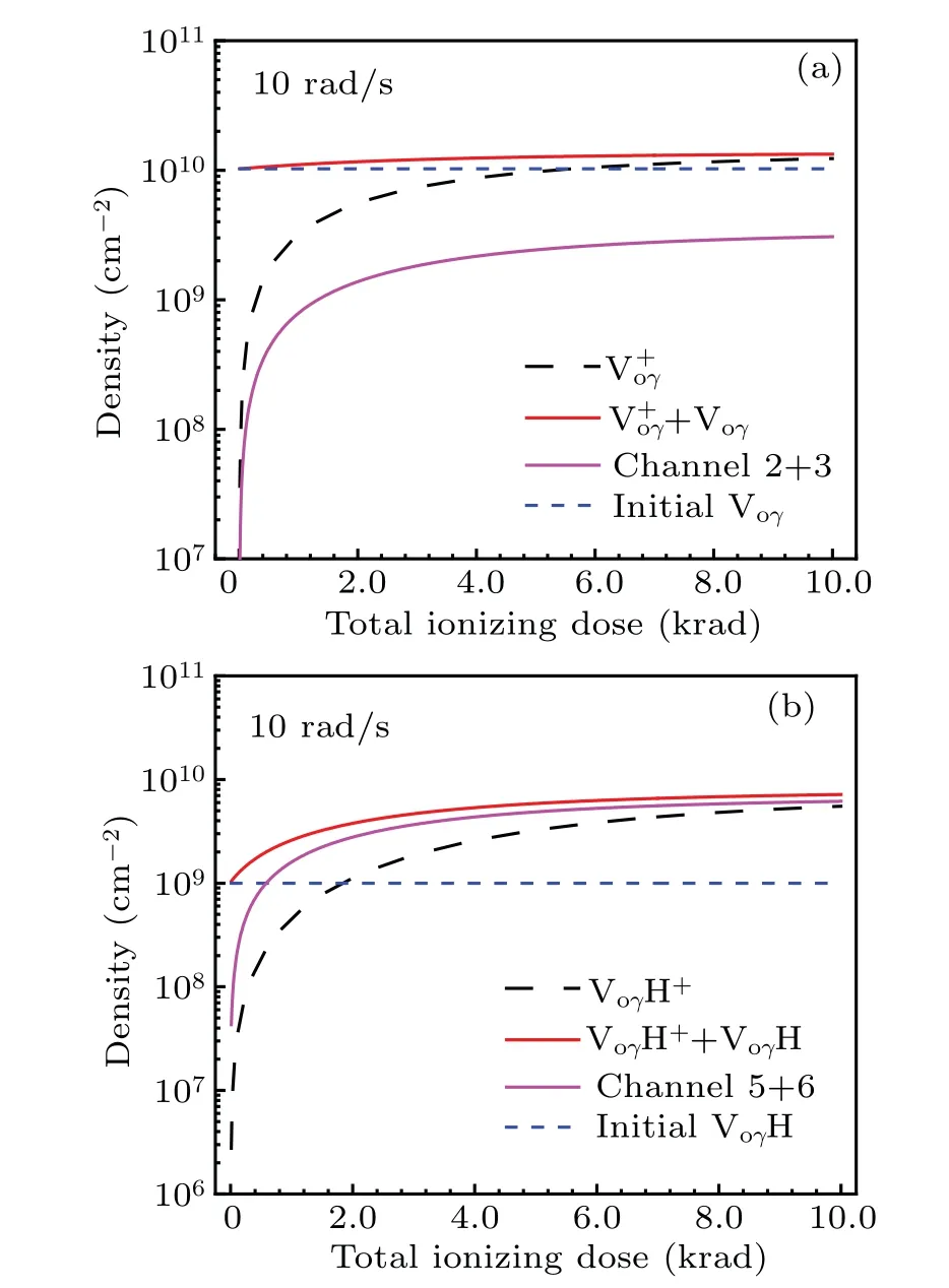
Fig.5.Density of(a)and(b)VoγH+in the oxide layer as a function of TID at the dose rate of 10 rad/s at 300 K.
In addition, the rise rates of the densities ofand VoγH+slow down with increasing TID, because the electric field inhibits the transport of holes and thus their formation rate. Figure 6(a) shows the spatial distributions of the electric fields under different TIDs. The electric fields near the gate/SiO2interface decrease with increasing TID,which slows down the transport of holes away from the gate. The electric fields near the Si/SiO2interface increase with increasing TID,which accelerates hole outflow from the oxide layer. The decrease in the density of holes in the oxide layer leads to a decrease in the probability of holes being captured to form charged defects. Therefore, with increasing TID, the growth rate of densities ofand VoγH+slows down.When the generation and consumption rates balance, their density tends to saturation. The ionization damage induced by the TID will reach saturation,which means that the TID effect has the maximum limit,and there are devices that can withstand the maximum damage. To further explore the influence of TID on the electric field at the interface, Fig.6(b)shows the relationship between the electric field at the Si/SiO2interface with TID.The electric field at the Si/SiO2interface (ESi/SiO2) increases with increasing TID (D), satisfying the universal 2/3 power law asESi/SiO2∝D2/3. The model is thus verified again by the 2/3 power law of the experiment.[38]As the TID increases,the threshold voltage decreases. It can also be seen from the figure that with increasing TID, the difference betweenESi/SiO2before and after irradiation is also increasing,which is as high as 17%of the initial electric field at 10 krad. For a typical grid in MOS devices,the electric field at the Si/SiO2interface can be simply described as follows:

whereVgis the gate voltage,Loxis the thickness of the oxide layer,ρtot≈kD2/3[38]is the density of space charge, andεoxis the relative permittivity of the oxide layer. The difference in the electric field is up to 17%after irradiation due to the contribution of space charges(mainlyand VoγH+). It means that the larger TID is, the larger ΔVthinduced by TID would be.
The whole process of threshold voltage shifts induced by TID is shown in Fig.7. The TID effect induces the generation of e-h pairs at first. In the case of positive gate voltage, the holes and electrons move towards the Si/SiO2and gate/SiO2interfaces, respectively. For the mobility of holes in SiO2is much slower than that of electrons, under the action of the electric field,the holes remain in the oxide layer. Meanwhile,most holes are captured by Voγto formduring movement, andare mainly accumulated near the Si/SiO2interface. The above processes will induce the built-in electric field,which enhances the total electric field at the Si/SiO2interface that satisfies the universal 2/3 power law with TID,and causes the increase of carrier density in the channel,resulting in the reduction of the threshold voltage of the MOS devices finally.
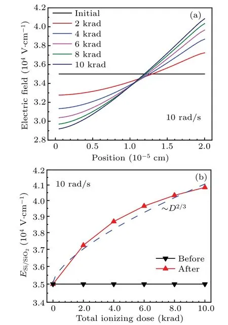
Fig.6. (a) Spatial distributions of the electric fields in the oxide layer under different TIDs. (b) Electric fields at the Si/SiO2 interface as a function of TID at the dose rate of 10 rad/s at 300 K.
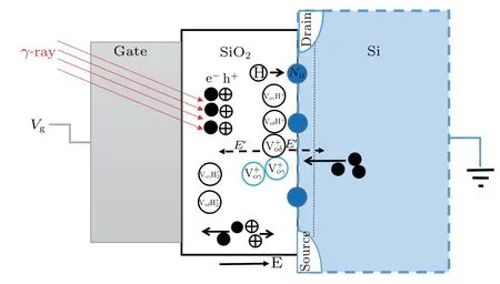
Fig.7. Schematic diagram of the threshold voltage reduction induced by TID.
3.3. Hardened methods for the threshold voltage shifts
From the analysis of Subsection 3.2,it can be seen that the electric field at the Si/SiO2interface plays a major role on ΔVthinduced by TID.Therefore,it is necessary to control the interfacial electric fields under different conditions to design high radiation-hardened devices. As shown in Eq.(13),in addition to the space charges mentioned above,there are the thickness(Lox)and the relative permittivity of the oxide layer(εox),the gate voltage (Vg), all of which are adjustable factors. In the following,we will investigate the influence of the above three factors(Lox,εoxandVg)on the electric field at the Si/SiO2interface,under the TID of 10 krad with the dose rate of 10 rad/s at 300 K.
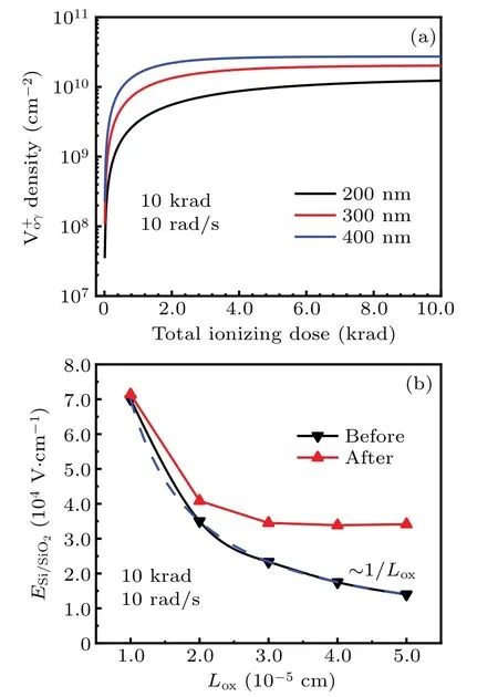
Fig.8. (a)Density of as a function of TID under the different thicknesses of the oxide layer.(b)Electric fields at the Si/SiO2 interface before and after irradiation as a function of the thickness of the oxide layer.
First, we simulated the influence ofLoxonandESi/SiO2. Figure 8(a) shows the change of the densities ofwith TID under differentLox. Under the same TID, the thinner the oxide layer,the lower the density ofin the oxide layer. Because the thinner the oxide layer is, the more easily the holes in the oxide layer flow out, which reduces the density of holes and their capture probability by Voγto form. In addition, asLoxincreases, it is faster forto tend to saturation,which also indicates that the thick oxide layer increases the capture probability of holes by Voγ, and thus increases the generation rate ofwhich will reach saturation faster. The change in density ofwill affect the electric field at the Si/SiO2interface. Figure 8(b) shows the electric fields at the Si/SiO2interface before and afterγ-ray irradiation as a function ofLox. After irradiation,with increasingLox,ESi/SiO2decreases and the decreasing rate slows down rapidly. There is an obvious inflection point at 200 nm. Less than 200 nm,ESi/SiO2is mainly contributed byEapplied,and the relationship ofESi/SiO2withLoxfollowsESi/SiO2∝1/Loxaccording to Eq.(13). Over 200 nm,ESi/SiO2is affected by both the increase ofEbuilt-inand the decrease ofEapplied.ESi/SiO2no longer satisfies the relationship of 1/Loxand is mainly controlled byEbuilt-in. In addition, with increasingLox, the difference betweenESi/SiO2before and after irradiation also increases, which means that the thickness of the oxide layer has a great influence on the electric field at the Si/SiO2interface after irradiation. Reducing the thickness of the oxide layer should be much beneficial to inhibit the reduction of the threshold voltage induced by TID.
In view of the influence of the permittivity of the oxide layer onandESi/SiO2,the densities ofwith TID at differentεoxare shown in Fig. 9(a). We found that the density ofalmost overlaps under differentεox, which means that changingεoxhas little influence on the density ofεoxafter irradiation. However,ESi/SiO2will decrease rapidly with increasingεoxas shown in Fig.9(b). This is because the permittivity changesESi/SiO2by changingEbuilt-inbutEapplied. Therefore,the relationship betweenESi/SiO2andεoxis the same as that ofEapplied,ESi/SiO2∝1/εoxaccording to Eq.(13). With increasingεox, the difference betweenESi/SiO2after and before irradiation becomes small. Thus,the permittivity has an obvious influence onESi/SiO2during irradiation.Increasing the permittivity could effectively inhibit the reduction of the threshold voltage induced by TID.
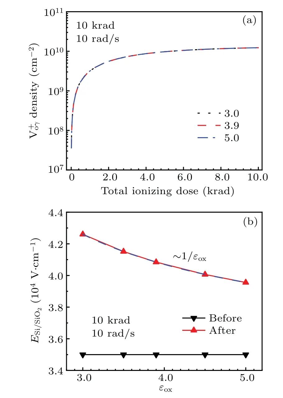
Fig.9. (a)Density of with TID at different relative permittivities.(b) Electric fields at the Si/SiO2 interface before and after irradiation with relative permittivity.
The influence of the gate voltage onandESi/SiO2is also studied. The densities ofwith TID at differentVgare shown in Fig.10(a). The higherVgis,the lower the density ofis in the oxide layer. It could be because the higherVgis,the greaterEappliedis in the oxide layer. The holes are easier to flow out, thus reducing the capture probability of holes by Voγto suppress the generation of. Moreover,with the decrease ofVg,reaches saturation faster, because the lowerVgincreases the probability of holes being captured by Voγto generate. Figure 10(b)shows the change ofESi/SiO2after and before irradiation and their ratios (ESi/SiO2/Eapplied) withVg. The ratio ofESi/SiO2/Eappliedincreases with decreasingVg.The ratio can be up to 2.5 whenVgis smaller than 0.4 V,and vanish whenVgis larger than 1.0 V becauseEbuilt-incan be neglected compared toEapplied. This means that the TID effect greatly influencesESi/SiO2whenVgis small. Thus, increasingVgcan effectively inhibit the harmful influence. As shown in Eq.(13),the slope ofESi/SiO2is related to the thickness of the oxide layer by 1/Lox,reducing the thickness can effectively reduce the harmful influence by TID.
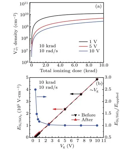
Fig.10. (a)Density of with TID at different gate voltages. (b)The interfacial electric field at the Si/SiO2 interface after and before irradiation and their ratio with the gate voltage.
4. Conclusions
In summary,we have developed a 1D dynamic model of mobile particles and defects in the oxide (SiO2) layer of a typical NMOS device underγ-ray irradiation, by combining rate equations and Poisson’s equation. The model is applied to simulate the distributions and evolution of charged defects and the electric field to reveal the key mechanisms of threshold voltage shifts induced by TID. The main process is the accumulation of V+oγinduced by TID near the Si/SiO2interface,which enhances the electric field at the interface and increases the carrier density in the channel by the electric field,thereby reducing the threshold voltage. Finally, considering these mechanisms,we pointed out that the oxide layer should be synthesized as thin as possible and with high enough permittivity in the oxidation process of device manufacturing.And the TID effects can be weakened by selecting devices with a higher threshold voltage.
Acknowledgements
Project supported by the Science Challenge Project of China (Grant No. TZ2018004), the National Natural Science Foundation of China (Grant Nos. 11975018 and 11775254),the National MCF Energy R&D Program of China (Grant No.2018YEF0308100),and the outstanding member of Youth Innovation Promotion Association CAS(Grant No.Y202087).
猜你喜歡
北京支部生活(2022年5期)2022-05-24 12:42:59
華人時(shí)刊(2022年23期)2022-05-10 08:19:28
Chinese Physics B(2022年3期)2022-03-12 07:44:30
東坡赤壁詩(shī)詞(2021年5期)2021-10-28 23:23:00
應(yīng)用數(shù)學(xué)(2021年1期)2021-01-07 01:24:36
廣東教學(xué)報(bào)·教育綜合(2019年11期)2019-09-10 17:56:29
Chinese Physics B(2017年9期)2017-08-30 08:26:32
小學(xué)教學(xué)研究·新小讀者(2015年10期)2015-12-05 05:54:22
快樂作文·低年級(jí)(2015年9期)2015-10-10 02:58:15
成都體育學(xué)院學(xué)報(bào)(2015年2期)2015-02-28 15:16:53
- Chinese Physics B的其它文章
- LAMOST medium-resolution spectroscopic survey of binarity and exotic star(LAMOST-MRS-B):Observation strategy and target selection
- Vertex centrality of complex networks based on joint nonnegative matrix factorization and graph embedding
- A novel lattice model integrating the cooperative deviation of density and optimal flux under V2X environment
- Effect of a static pedestrian as an exit obstacle on evacuation
- Chiral lateral optical force near plasmonic ring induced by Laguerre–Gaussian beam
- Adsorption dynamics of double-stranded DNA on a graphene oxide surface with both large unoxidized and oxidized regions