
Surface modulation of halide perovskite films for efficient and stable solar cells
2022-03-12 07:50:04QinxuanDai戴沁煊ChaoLuo駱超XianjinWang王顯進(jìn)FengGao高峰XiaoleJiang姜曉樂(lè)andQingZhao趙清
Chinese Physics B 2022年3期
關(guān)鍵詞:高峰
Qinxuan Dai(戴沁煊) Chao Luo(駱超) Xianjin Wang(王顯進(jìn)) Feng Gao(高峰)Xiaole Jiang(姜曉樂(lè)) and Qing Zhao(趙清)
1Key Laboratory of General Chemistry of the National Ethnic Affairs Commission,School of Chemistry and Environment,Southwest Minzu University,Chengdu 610041,China
2State Key Laboratory for Mesoscopic Physics and Frontiers Science Center for Nano-optoelectronics,School of Physics,Peking University,Beijing 100871,China
3Peking University Yangtze Delta Institute of Optoelectronics,Nantong 226010,China
Keywords: perovskite solar cells,interfacial engineering,surface modulation,organic salt surface layer
1. Introduction
Halide perovskite solar cells(PSCs)are on their way towards the urgent requirement of low-cost renewable clean energy. Halide perovskites are a kind of semiconductors commonly with the formula ofABX3, whereAis monovalent cations of MA+(CH3NH+3),FA+(NH2-CH=NH+2)and Cs+,Bis divalent cations of Pb2+and Sn2+, andXis halides of I-, Br-and Cl-.[1-3]These materials have been demonstrated to have excellent photoelectric properties such as high light absorption coefficient, long carrier lifetime and diffusion length,high carrier mobility,low exciton binding energy,and adjustable band gap.[3-9]These advantages make halide perovskites very suitable for light absorbers in solar cells.[10]Based on rich experience in dye sensitized solar cells,organic solar cells, thin film solar cells and silicon solar cells, great progresses have been obtained on PSCs. Device configurations are the basic for fabricating PSCs,[11]halide perovskites were initially adopted as dyes in dye sensitized solar cells in the form of quantum dots.[12]Now they are mostly in the form of thin films sandwiched between selective contact of charge transport layers (CTLs), forming n-i-p PSCs with the electron transport layer(ETL)deposited on the window substrate and p-i-n PSCs with the hole transport layer(HTL)deposited on the window substrate. The p-i-n PSCs are also commonly called inverted PSCs. The concept of planar and mesoscopic PSCs, which is determined by whether the functional layer is in the form of planar type or mesoscopic type, is also put forward. To improve the photovoltaic performance of PSCs,large deals of researches are focused on the morphology control and composition optimization of halide perovskite films,a kind of device configuration.[13-18]Therefore,the efficiency of PSC has been rapidly improved in recent years and the highest certificated PCE for PSCs had been boosted to 25.5%.[19]Recent papers also reported certificated PCE of 25.2% for both planar and mesoscopic n-i-p PSCs.[20,21]In addition to PCE,PSCs’life span had been also greatly enhanced from minutes to hundreds and thousands of hours.[22-29]Further pushing PSCs towards outdoor applications in the near future is widely expected.
In addition to morphology and components,the interface is also critical to the photovoltaic performance of PSCs, as has been demonstrated in efficient silicon solar cells and other semiconductor devices with various interface structures.[30-32]Due to the imperfection of crystals at the interfaces, defects are formed and bring nonradiative recombination, leading to efficiency loss. Moreover, interface is the initial entrance for water to degrade the perovskite lattice. PSCs have interfaces between halide perovskite films and adjacent charge transport materials together with interfaces between charge transport materials and electrodes. Those interfaces can be modulated to optimize the performance of PSCs. On one hand, these interfaces are constructed by the adjacent layers. Therefore,adjusting the chemical compositions, surface properties and electronic properties of functional layers in PSCs can influence the properties of the interfaces.[33-37]On the other hand,the interfaces can be also modulated by inserting an additional interface layer.[38-40]Among various interfaces in PSCs,those related to perovskite films are more concerned.[41,42]
Two interfaces including the bottom and the top interfaces are related to perovskite films(Fig.1). The bottom interface is near the substrate on which the perovskite film is deposited,[43]which is greatly influenced by the surface electronic properties of the under layer. The top interface is on the top of perovskite films and in contact with the hole transport layer for n-i-p PSCs or electron transport layer for p-i-n PSCs.[44]This interface can be adjusted by modulating the surface of the perovskite film. Modulation of both interfaces has contributed a lot to various breakthroughs of PSCs. Tanet al.introduced chloride on top of TiO2and passivated defects at the interface between TiO2and the halide perovskite,boosting the PCE of n-i-p planar PSCs to 21.4%.[35]Jianget al.treated the top surface of perovskite films with phenethylammonium iodide(PEAI)to passivate defects at the interface,boosting the PCE of n-i-p planar PSCs to a record of 23.32%.[44]Yooet al.obtained a certificated PCE of 25.2% for n-i-p planar PSCs by treating the top surface of perovskite films with alkylammonium bromide.[20]Luoet al.treated halide perovskite films with guanidinium bromide to make the surface more n type,boosting the PCE of inverted p-i-n planar PSCs to approach 21%.[45]Wanget al.treated CsPbI3film with choline iodine,boosting the PCE of n-i-p planar inorganic PSCs to 18.4%.[46]Jeonget al.obtained a certificated PCE of 25.2% for n-i-p mesoscopic perovskite solar cells by treating perovskite films with octylammonium iodide (OAI).[21]Optimizing the interface has also contributed a lot to the stability enhancement of PSCs.[26,39,47]Although both interfaces have been optimized to improve the performance of PSCs, the top interface gains more attention since the surface of halide perovskite films can be modulated more easily. Various chemicals,including salts,small molecules, polymers, metal oxides and nano particles have been adopted to construct top interface layers for PSCs.Among those chemicals,halide salts are the most widely used.They can form several kinds of interface layers with halide perovskite films and have contributed a lot to the PCE and stability enhancement of PSCs(Fig.1 and Table 1).
In this review,we focus on progresses on modulating the top surface of perovsktie films via halide salts for efficient and stable PSCs. We summarize attempts on constructing threedimensional (3D) halide perovskite graded junction layer for better energy level alignment and preferred carrier transport in PSCs to enhance the charge extraction efficiency. We also review the popular work of treating halide perovskite films with organic halide salts to construct low-dimensional halide perovskite interface layer and interface passivation layer to suppress non-radiative recombination. We expect these results could provide guidance for further research on more efficient interface modification toward more efficient and stable PSCs.
2. Constructing a 3D halide perovskite graded junction interface layer
Constructing a graded junction in solar cells is beneficial for optimizing energy level alignment to enhance built-in electric field,which could help to enhance preferred extraction of carriers and suppress nonradiative recombination by inhibiting the undesired diffusion of photogenerated carriers.[73]Although the built-in electric field in PSCs is generally formed by the n-type electron transport layer and the p-type hole transport layer,a proper graded junction layer can still make sense.An important property of halide perovskites is that their compositions can be adjusted accordingly, and the perovskites with different compositions possess different bandgaps, energy band structures and electronic properties.[3]Therefore,a graded interface junction on perovskite films can be designed flexibly based on component regulation to enhance the performance of PSCs.
Liet al.constructed a graded heterojuction by preparing CsPbBrxI3-xlayers with variedxfrom 0 to 0.7 on the top of MAPbI3film, which enhanced the PCE of hole-conductorfree PSCs from 8.16% to 11.33% (Figs. 2(a)-2(c)).[48]Holeconductor-free PSCs are a type of device which does not adopt conventional hole conductors such as Spiro-OMeTAD,PTAA or NiO.[22,74]Such devices benefit a lot from the excellenthole transport properties of halide perovskites and are developed to reduce the cost and improve the stability of conventional PSCs.[75]However,due to the absence of hole conductors,charge extraction between perovskite and the electrode is significantly restricted and charge recombination is also much more serious at the interfaces than conventional PSCs,leading to much lower PCE.[76]Tailoring energy band alignment via the formation of graded junction in those devices holds potential to improve the PCE of hole-conductor-free PSCs. To build the graded heterojunction in the hole-conductor-free PSCs,the CsPbBrxI3-xnanocrystals were first prepared and then spin coated on the MAPbI3films. CsPbBrxI3-xnanocrystals have larger bandgap than MAPbI3and their conduction band minimum (CBM) and valence band maxium (VBM) are higher than those of MAPbI3. When stacked on top of MAPbI3,the graded heterojunction was formed,which could direct the flow of electrons and holes to the preferred direction. Moreover,the Br contents in CsPbBrxI3-xnanocrystals were further varied to form different compositions with different energy band structures. It is found that the higher the Br content is, the higher the CBM and the VBM are. Based on this characteristic,the grade of the junction was further increased from 1 to 2,3 and 4 to help create the hole channel and provide more energy barriers to reduce the reverse photocurrent inside the devices. The multi graded heterojunctions enhanced the hole extraction efficiency and charge transport in the devices. Generally,Br can exchange with I to form mixed halide perovskites,which could make the bandgap of MAPbI3become larger.[77]Here,the monochromatic incident photon-to-electron conversion efficiency(IPCE)results indicated that the bromide in the nanocrystals did not substitute iodide in the active layer significantly.Thus,the absorption region of the device derived from IPCE was not changed when CsPbBrxI3-xnanocrystals were introduced. As a result,the PCE of hole-conductor-free PSCs was significantly improved. Similarly, Yuanet al.also constructed a graded homojunction by stacking CsPbI3perovskite quantum dot layers with different bandgaps and boosted theVOCof the device to 1.25 V.[49]Chenget al.explored the multiple functions of CsPbBrxI3-xquantum dot layer on perovskite films.[50]They found that the QD surface layer could reduce trap states,assist the formation of preferred energy level alignments and affect the morphology and charge transport properties of HTLs.These positive effects benefited the performance of PSCs significantly.

Table 1. Summary of top interface layer constructed by halide salts for PSCs.
The evaporation rather than solution-processed method to stack FAPbIyBr3-yon top of CsPbIxBr3-xwas also adopted by Zhanget al.to prepare graded perovskite layers for optimizing energy band alignment.[51]They found that the CBM and VBM of evaporated FAPbIyBr3-ywere higher than those of CsPbIxBr3-x. Such energy band structure optimized the energy-band alignment and improved the device’s PCE from 14.61% to 17.48% with higher open circuit voltage (VOC),short circuit current density (JSC) and fill factor (FF). With a similar conceive but more facile method,Liuet al.realizedin situgrowth of perovskite stacking layers for hole-conductorfree PSCs with carbon electrodes (Figs. 2(d)-2(f)).[52]In this method, MABr was spin coated directly onto the asprepared MAPbI3layer with excess PbI2. The excess PbI2mostly presented on the top surfaces or at the boundaries and reacted with MABr toin situform MAPbxBr3-x. The spectrum of MAPbI3/MAPbIxBr3-xfilm exhibited a slight blue shift when compared with MAPbI3film, probably due to ion exchange and penetration of Br. The Fermi level of MAPbI3/MAPbIxBr3-xfilm shifted upward for about 0.31 eV when compared with MAPbI3film, and the VBM and CBM shifted upward of about~0.23 eV and~0.25 eV accordingly. The changed surface energy band structure affected the charge carrier dynamics by optimizing the energy level alignment in the devices, and enhanced the charge transport and suppressed the charge recombination. As a result, the backward scanning PCE of the device was booted from 11.3%to 16.2%. Ruanet al.also realized thein situgrowth of MAPbI3/MAPbIxBr3-xfilm for hole-conductor-free PSCs.[53]The MAPbIxBr3-xlayer was prepared by evaporating MABr onto the MAPbI3layer to substitute partial iodide with bromide. The authors demonstrated that the MAPbIxBr3-xlayer could work as an electron blocking layer which aligned the energy level alignment between the metal electrode and MAPbI3,and blocked charge recombination at the interface. The devices’ PCE was enhanced from 12.05% to 17.36% with theVOCincreased from 936 mV to 1047 mV.
Except for halide regulation,theBsite cation can be also adjusted to form graded junction in PSCs. Generally,B-sites cations for halide perovskites include Pb and Sn. Sn-based perovskites prefer to behave as p-type semiconductors.[78]Sunet al.designed a graded homojunction in PSCs by coupling a 1.53 eV n-type bottom lead-based perovskite layer and a 1.27 eV p-type top mixed Pb/Sn perovskite layer(Fig.3).[54]To fabricate the graded junction, PbI2layers were deposited first, then organic halide salts containing FAI, MABr and MACl were deposited.SnI2dissolved in anisole,which would not dissolve the bottom perovskite, was deposited lastly. An interesting phenomenon was that the absorption region of the graded Pb/Sn perovskite red-shifted to some extent but showed no obvious absorption edge. The stabilized PCE of the graded Pb/Sn perovskite-based device was 20.98%,which was much higher than the mixed Pb/Sn-based devices and the Pb-based devices. Moreover, the graded junction weakened the influence of charge transport layers(CTL)on PSCs’performance(Fig.3(c)). CTL in PSCs can not only extract photo-generated charges, but also suppress charge recombination. The weakened influence indicated that the graded heterojunction could serve as CTL and promoted oriented carrier transport.

Fig.2. (a)Schematic diagram for device structure;(b)schematic diagram for charge transport,and(c)device performance of hole-conductor-free solar cells with graded CsPbBrxI3-x layers.[48] (d)Schematic diagram for device structure,(e)schematic diagram for energy diagram,and(e)PCE distribution of hole-conductor-free PSCs with in situ grown graded MAPbIxBr3-x.[52]
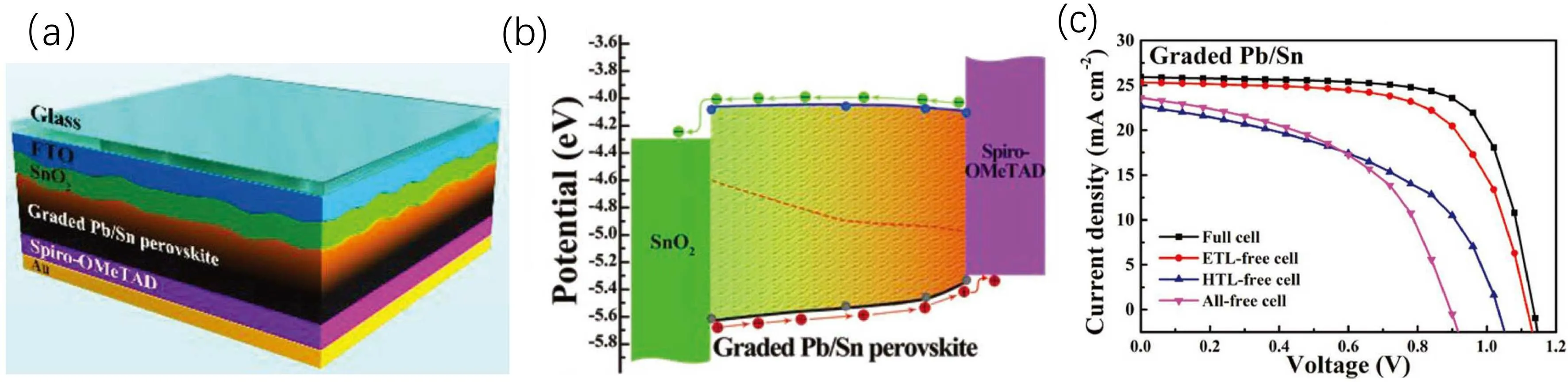
Fig.3. (a)Schematic diagram for the device structure,(b)schematic diagram for charge transport and(c)device performance of PSCs with graded Pb/Sn junction.[54]
In addition to the above methods to construct the graded junction by introducing differentA-site cations,B-site cations orX-site anions to form different halide perovskites, halide perovskites can also be doped to form graded junction. Previous studies have demonstrated that halide perovskites can be self-doped by non-stoimetric compositions.[79,80]When lead iodide in halide perovskites is excessive, the prepared perovskites tend to be n doped.When halide organic salt is excessive, the prepared perovskites tend to be p doped. Luoet al.prepared a more n-type perovskite film via solution-processed secondary growth (SSG) technique for inverted planar perovskite solar cells and improved the stabilized PCE of the inverted PSCs to 21%.[45]The SSG was conducted by coating guanidinium bromide (GABr) on the perovskite films for secondary growth. GABr digested the residual PbI2in the perovskite films and led to over 100-meV shift of the surface potential. Such treatment made the perovskite films more n-type by decreasing their work function from 5.02 eV to 4.42 eV. The more n-type feature brought occupation of vacant traps in perovskite films and reduced trap-assisted recombination. Meanwhile, the more n-type perovskite films were also beneficial for charge selections from the surfaces. These benefits suppressed non-radiative recombination in SSG perovskite films with greatly increased photoluminescence quantum yield. As a result,the surface treatment reduced inverted PSCs’voltage loss to 0.41 V and led to a highVOCof 1.21 V,which is 100 mV higher than that of the devices without treatment.
Cations in some halide salts could also substitute lead in halide perovskites to induce n-doping.Luet al.realized n doping of halide perovskites’ surface via treating with InBr3for planar inverted perovskite solar cells.[55]Bromide substituted the iodide while In3+substituted Pb2+and donated an electron for n doping. Such doping led to the optimized energy level alignment by an intriguing n/n+homojunction, resulting in the enhancement of built-in electric field and reduction of electron injection barrier. Similarly, Huanget al.incorporated Sb as shallow donors to n-dope halide perovskites.[81]The n-doping also led to the formation of enhanced built-in electric field for ETL-free PSCs and improved the device’s PCE to 12.62%. In addition to n-doping, Noelet al.realized p doping of halide perovskite by treating perovskite films with the strongly oxidizing molybdenum tris(dithiolene) complex of Mo(tfd-COCF3)3,[82]which increased the work function of the halide perovskites from 4.67 eV to 5.13 eV.The optimized energy band alignment enhanced charge extraction at the interface and boosted the PCE to near 21%.
3. Constructing a low-dimensional halide perovskite interface layer
In addition to preparing a graded halide perovskite on top of halide perovskite films, a low-dimensional halide perovskite surface layer can also be beneficially constructed to improve the efficiency and stability of PSCs. Lowdimensional halide perovskites including two-dimensional(2D) and quasi-two-dimensional halide perovskites are important derivatives of common three-dimensional(3D)halide perovskites.[83,84]These low-dimensional halide perovskites are formed by replacing commonAcations including MA,FA and Cs inABX3with larger organic cations such as butylammonium(BA)and PEA,whose ion sizes exceed the tolerance limit of 3D perovskites,thus those larger organic cations serve as spacers to slice the 3D perovskites in specific crystal planes to form two-dimensional perovskites. One typical formula of low dimensional halide perovskites is (A′)2An-1BnX3n+1,known as the Ruddlesden-Popper(R-P)halide perovskites.[85]Thenrepresents the number of PbI4-6 layers between twoA′layers. Whenn= ∞, the R-P perovskites become 3D perovskites. The properties of R-P perovskites can be adjusted by changing theA′cations andn. A lot of studies have demonstrated that low-dimensional perovskites have much better stability than those 3D perovskites, especially the stability against moisture.[86-89]The bandgaps of lowdimensional perovskites are generally larger than their 3D analogues. Based on these characteristics, constructing a thin RP perovskite layer on 3D perovskite films has been explored and demonstrated to be very effective for efficient and stable PSCs.[56-58,90-92]
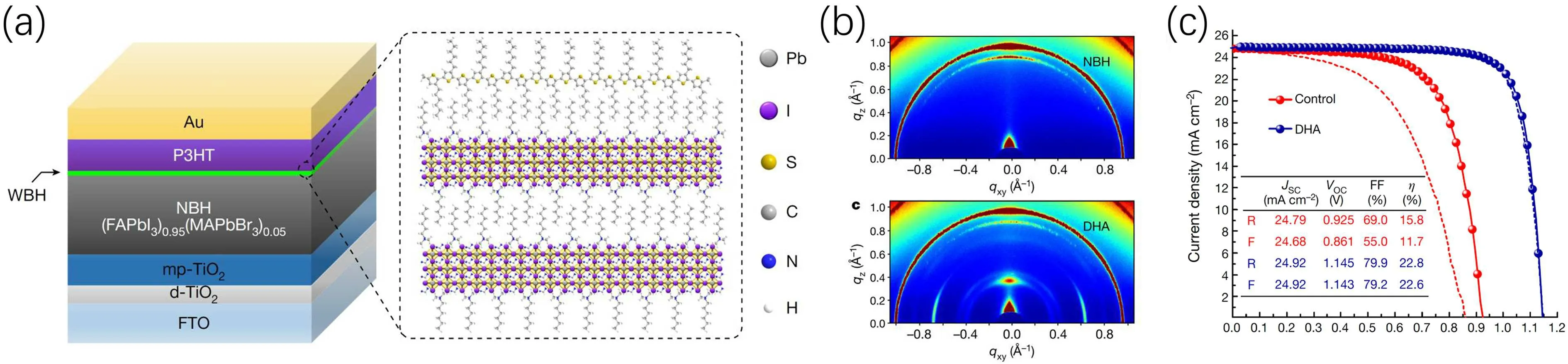
Fig.4.(a)The device structure of n-i-p perovskite solar cells based on the P3HT hole transport material with the low-dimensional halide perovskite interface layer formed by HTAB.(b)GIWAXS patterns of halide perovskite films with and without the low-dimensional halide perovskite interface layer. (c)Performance comparison of n-i-p perovskite solar cells based on the P3HT hole transport material with and without the low-dimensional halide perovskite interface layer.[47]
Junget al.fabricated efficient and stable perovskite solar cells by preparing a thin wide-bandgap halide perovskite layer(WBH)on the narrow-bandgap perovskite films(NBH)(Fig. 4).[47]The WBH was formed by spin coating n-hyxyl trimethyl ammonium bromide (HTAB) on the NBH surface to form the double-layered halide perovskite structure(DHA).The formation of low-dimensional WBH was demonstrated by the 2D grazing-incidence wide-angle x-ray scattering(GIWAXS) patterns, which exhibited a distinct signal atqzof 0.39 °A-1. The WBH layer was about 12 nm thick and found to prolong the charge lifetime in the devices significantly.More importantly, the WBH layer led to self-assembled poly(3-hyxylthiophene) (P3HT) hole transport layer and affected its morphology and electronic properties, thus violently enhanced the HTL’s mobility from 10-5cm2·V-1·s-1to 0.1 cm2·V-1·s-1. The self-assembling of P3HT was considered to be induced by the interaction alkyl chain in HTAB with P3HT polymer. The PCE of PSCs was also improved from 15.8% to 23.3% with improvedVOCfrom 0.925 V to 1.145 V and released hysteresis. Moreover, the WBH layer improved the operational stability of PSCs, maintaining 95%of the initial PCE after 1370 h, while the control PSCs degraded seriously within 100 h.
Liuet al.adopted pentafluoro-phenylethylammonium(FEA) cations to form a low-dimensional perovskite surface layer of (FEA)2PbI4on 3D perovskite films (Fig. 5(a)).[59]FEA cations were introduced by dipping the 3D perovskite films in FEAI’s solution and the thickness of the surface layer was about 9 nm. (FEA)2PbI4had a superhydrophobic character, which decreased the perovskite film’s surface energy effectively and reduced unencapsulated PSCs’ efficiency loss from 57% to 10% after working at maximum power point for 1000 h under light soaking in ambient condition with humidity of 40%. Moreover, the (FEA)2PbI4layer improved the PCE of PSCs from 20.62% to 22.16%with enhancedVOCfrom 1.045 V to 1.096 V. Similarly,Chenet al.treated hole-conductor-free perovskite solar cells with FEAI to form low-dimensional halide perovskite interface layer between carbon and three-dimensional halide perovskite, boosting the PCE to 17.47%.[60]Zhanget al.found that the introduction of fluorine shortened the average phenyl ring centroid-centroid distances and enhanced charge transport across adjacent inorganic layers.[93]This would make FEAI more suitable for the low-dimensional halide perovskite interface layer. Choet al.synthesized a new fluorosis organic cation (CH3)3CO(CH2)3NH+3(A43) to form lowdimensional perovskite surface layer on top of 3D perovskite films (Fig. 5(b)).[94]In addition to depositing A43 solution directly onto 3D perovskite films for the formation of lowdimensional layer, it is also demonstrated that adding A43 into the 3D perovskite precursor could also lead to the formation of low-dimensional surface layer due to phase segregation. The A43 surface layer improved the hydrophobicity of the perovskite films. The surface layer also improved the PCE of PSCs from 17.98%to 20.13%withVOCfrom 1.04 V to 1.11 V.Sutantoet al.eliminated interfacial recombination losses in hybrid perovskite solar cells by constructing 2D/3D perovskite interfaces via the 2-TMABr salt(Fig.5(c)).[95]The interface formed a p-n junction and reducedVOClosses at the interface in PSCs, resulting in aVOCof 1.19 V which was touching the potential theoretical value.
Solution-processed methods for preparing the lowdimensional perovskite layers are mainly based on isopropyl alcohol(IPA)solvent. Yooet al.found although it was commonly believed that IPA did not dissolve halide perovskites seriously, IPA could in fact degrade halide perovskite films.[62]IPA dissolves organic salts such as FAI effectively and treating perovskite films with IPA led to the formation of PbI2.[96]Therefore, developing a solvent which can dissolve organic salts for low-dimensional perovskite and can not dissolve halide perovskites is of great importance for surface treatment of 3D perovskite films. Yooet al.found that an antisolvent of chloroform(CF)was a good choice since it can dissolve n-hexylammonium bromide(C6Br)for low-dimensional perovskites very well and dissolve halide perovskite little(Fig.5(d)).[62]Treating with C6Br in CF suppressed the nonradiative recombination and improved the device performance from 21.3%to 22.3%.Needing to point out,other antisolvents including chlorobenzene and toluene can not dissolve either halide perovskites or C6Br,indicating they can not be applied to replace CF.From this point of view,once an organic salt is selected for low-dimensional halide perovskites,it is better to develop a well compatible solvent system which can dissolve the corresponding organic salt but can not dissolve the halide perovskites.
Besides spin coating and dipping, Janget al.developed a solid-phase in-plane growth method to prepare a 2D perovskite surface layer for efficient and stable PSCs(Fig. 6).[63]This method benefits from the ion migration and exchange properties of halide perovskites. As shown in Fig. 6, the 2D (BA)2PbI4perovskite film and the 3D(FAPbI3)0.95(MAPbBr3)0.05perovskite film were firstly prepared on substrates respectively. Then, both films were stacked under pressure and heated for a period of time to induce the nucleation and growth of 2D perovskite layer on 3D perovskite films. Compared with solution-processed methods,such solid-state reaction avoided the formation of unintended phases and made the thickness control of 2D perovskite layer more conveniently. The(BA)2PbI4surface layer reduced surface trap-assisted non-radiative recombination and improved the charge lifetime in(FAPbI3)0.95(MAPbBr3)0.05from 0.2 μs to 1.1 μs. Besides,the(BA)2PbI4surface layer exhibited typical p-type semiconductor properties and formed p-p isotype heterojunction with the 3D perovskite, which increased the built-in potential(Vbi)of the device from 1.087 V to 1.194 V.As a result,the PCE of the device was improved from 22.39%to 24.59%withVOCincreased from 1.098 V to 1.185 V.
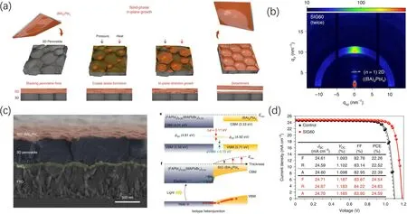
Fig.6. (a)Schematic diagram of the solid-phase in-plane growth method of(BA)2PbI4 interface layer for PSCs. (b)GIWAXS signals for the(BA)2PbI4 interface layer. (c)The cross-sectional image,energy level bending and(d)device performance of PSCs with(BA)2PbI4 interface layer.[63]
4. Constructing a halide salt interface layer
Halide salts are introduced to not only form the lowdimensional perovskite interface layer,but also form an interface layer to passivate surface traps, together with forming a hydrophobic layer and even stabilizing metastable perovskite phase of CsPbI3and FAPbI3.[64,97,98]Passivating defects at the interfaces is an important strategy to improve the performance of solar cells,as has been well demonstrated in various kinds of silicon solar cells. For PSCs, the perovskite films are generally polycrystalline and abundant of defects are located on the surfaces and grains boundaries. With the morphology and composition of halide perovskite films being optimized better and better,those defects,which lead to obviousVOCloss,become the main constraint that limits the PCE of PSCs towards the theoretically Shockley-Queisser limit for single-junction non-concentrated solar cells. Therefore, developing efficient strategies to passivate these defects in PSCs is very important and draws intensive attention. Introducing halide salts with large organic cations to incorporate with halide perovskite to improve PSCs’performance has been tried long,and they are demonstrated effective again and again for defect passivation and performance enhancement.
PEA and their derivatives are the mostly adopted organic cations for the interface layer.Wanget al.treated FAPbI3films with amines,benzylamine and phenethylamine,and found that the amines especially the benzylamine could stabilize the perovskite films for months in moisture air due to the hydrophobic aromatic group.[97]In this work,the applied species is the amines,rather than their halide salts.Liet al.prepared FAPbI3films via sequential deposition method and added some PEAI in the FAI solution.[99]It is found that PEAI passivated defects at lattice surface and grain boundaries. Meanwhile,PEAI increased the energy barrier for the transformation of black FAPbI3to yellow FAPbI3and also improved the hydrophobicity of the perovskite films. As a result, the stability and PCE of FAPbI3PSCs were enhanced significantly.Liet al.also treated cesium-containing perovskite films with PEAI and demonstrated the improved moisture resistance of the films.[65]Similarly, Yooet al.found that treating perovskite films with PEAI can effectively improve the lifetime of carriers and release hysteresis of the fabricated PSCs.[66]
More importantly, by treating the surface of FA-MA based perovskite films with PEAI, Jianget al.obtained a certificated PCE of 23.32% withVOCloss of only 0.35 V,and broke the efficiency record of planar PSCs (Fig. 7).[44]Ideal factor, lifetime of photogenerated carriers and transient photovoltage measurements of the fabricated devices clearly demonstrated the effective passivation effect. In this work,the authors also attempted to clarify whether it is PEAI itself or the low-dimensional halide perovskite formed by PEAI that contributed to the PCE enhancement. It was found that depositing PEAI at room temperature without annealing increased the carrier lifetime from 0.3 μs to 2 μs.While,when the PEAI was annealed,the PL lifetime decreased to be similar with the control sample. This result suggested that annealing removed the passivation effect of PEAI.XRD results showed that annealing led to the formation of low-dimensional PEA2PbI4.Therefore,it is PEAI itself that has much better passivation effect rather than the low-dimensional perovskite.
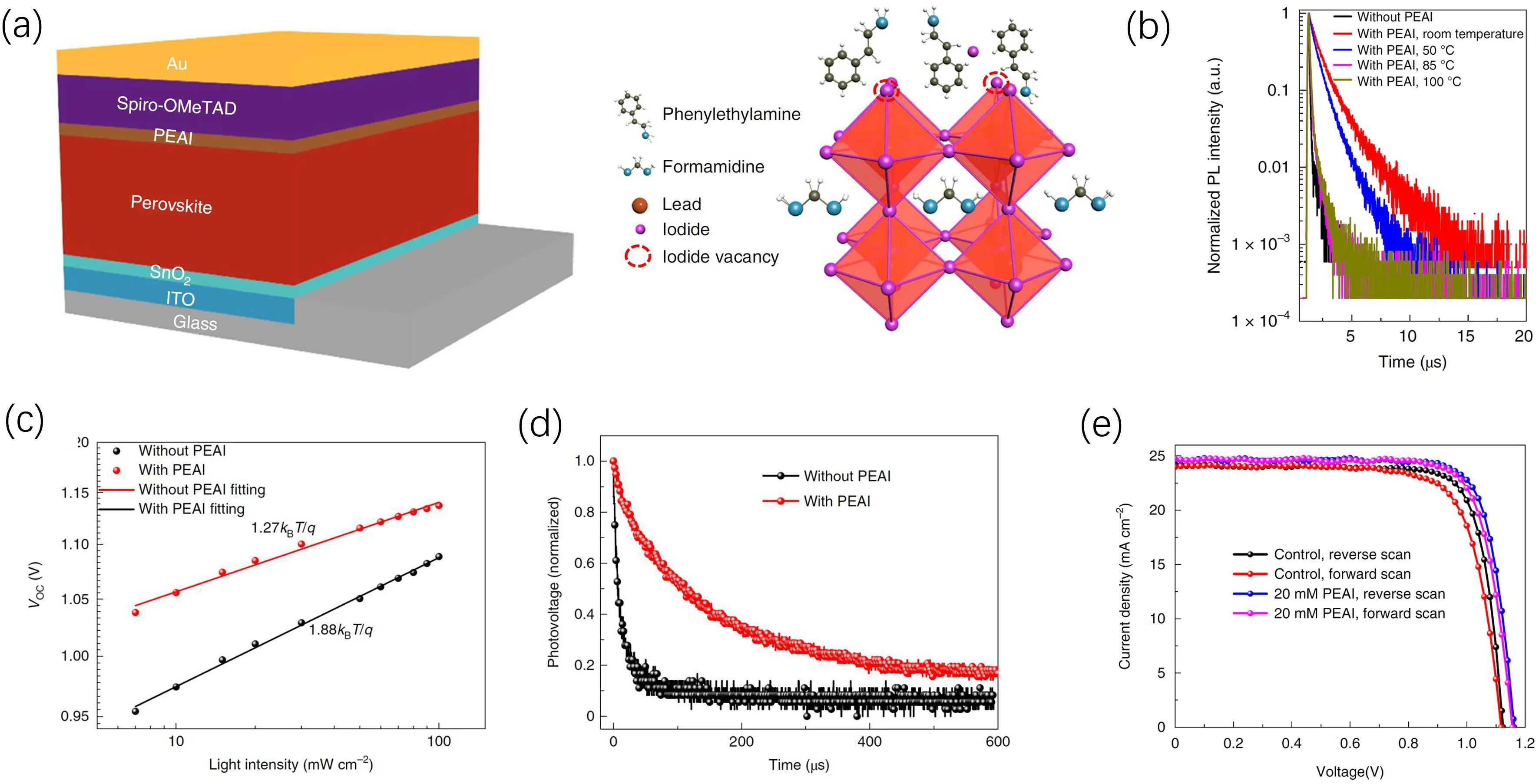
Fig.7. (a)The device structure of planar n-i-p PSCs with a PEAI interface passivation layer. (b)Influence of annealing temperature on PEAI’s passivation effect. (c)Ideal factor,(d)transient photovoltage and(e) j-V curves of planar PSCs with and without the PEAI interface passivation layer.[44]

Fig. 8. (a) Chemical structures of PEA’s derivatives with different functional groups for interface passivation layer of PSCs.[67] (b) Chemical structure of passivation molecules with marked amino (blue) and carboxyl (red) groups.[100] (c) HBAI for PSCs’ interface passivation layer.[68](d)Chemical structure of Choline salts for PSCs’interface passivation layer.[101]
Making clear what characteristics of the cations influences the passivation effect is the key to select or design organic cations. Zhuanget al.studied the electron density of the benzene ring on the passivation effect by introducing electron-donating groups or withdrawing groups to PEA(Fig.8(a)).[67]The results indicated that the electrostatic interaction between benzene ring and the under-coordinated Pb2+was responsible for the defect passivation. Electrondonating groups were more beneficial for the electrostatic interaction. PEAI containing methoxyl(CH3O-PEAI),which is a typical electron-donating group, led to the increasement of carrier lifetime from 0.95 μs to 2.93 μs withVOCincreased from 1.11 V to 1.18 V and PCE increased from 19.98% to 22.98%. Yanget al.tailored the molecular structures of the organic passivators by varying functional groups for inverted PSCs (Fig. 8(b)).[100]They found that negative and positive defects in halide perovskites could be passivated by carboxyl and amine groups via the electrostatic interaction while the aromatic structures could passivate the neutral iodine defects.Based on such finding,D-4-tert-butylpheneylalanine(D4TBP)with both amino and carboxyl groups was designed as a new passivator and led to aVOCof 1.23 V withVOCdeficit of 0.34 V for 1.57-eV perovskite.
Yanget al.applied the mixture CF3(CF2)2CH2NH3I(HBAI) and FAI to treat the surface of perovskite films and passivated the surface traps effectively (Fig. 8(c)).[68]Meanwhile, the surface layer optimized the energy level alignment and enhanced the charge extraction. The PCE of the device was boosted to 23% with average 80 mVVOCenhancement. Quaternary ammonium salts were also demonstrated effective for post treatment to passivate defects on the surface of perovskite films. Zhenget al.found that ammonium halides NR+4X-could passivate ionic defects in halide perovskites with their negative- and positive-charged components.[64]Treating perovskite films with choline chloride improved the PCE of inverted p-i-n PSCs to a certified value of 20.59%with reducedVOCdeficit of 0.39 V.Wanget al.found that treating the surface of inorganic CsPbI3halide perovskite with choline iodide could passivate defects and adjust the energy level alignment at the interfaces at the same time, leading to a big progress of inorganic perovskite solar cells with a stable efficiency of 18.4%.[46]Luet al.treated FAPbI3films with choline chloride to passivate defects and reducedVOCdeficit of PSCs to as low as 0.33 V(Fig.8(d)).[101]Other studies demonstrated that not only large cations can be applied as the surface treatment layer, MAI can also be adopted. Hawashet al.deposited an ultrathin MAI layer on MAPbI3films to optimize the interface energetics and enhance the device performance.[69]Songet al.prepared atomistic surface passivation of MAPbI3via MAI for x-ray detectors and realized high sensitivity.[102]
In addition to the passivation effect,the functional groups of the passivators can be also adjusted to enhance device stability against moisture and heat. Oliveret al.found that benzylammonium bromide brought more stable passivation effect than PEAI at high temperature.[103]Zhuet al.introduced 4-tert-butyl-benzylammonium iodide(tBBAI)passivator and retarded nonradiative charge carrier recombination significantly,improving the PCE from 20% to 23.5% (Fig. 9(a)).[70]The tert-butyl group improved the hydrophobicity of perovskite against moisture and improved the long-term operational stability of the device. Fluorine was introduced to further improve the hydrophobicity of the passivator. Liet al.introduced 4-(Trifluoromethyl)benzylamine (TFMBA) to form an ultrathin passivation layer (Fig. 9(b)). Benefiting from the hydrophobic benzene ring and fluorinated alkyl group, unencapsulated PSCs maintained 84% of the initial PCE after aging under 65%-75% humidity of 1300 hours.[104]Zhuet al.also greatly enhanced the stability and PCE of PSCs with the help of TFMBA passivation layer which boosted the PCE from 20.9%to 23.9%. The device retained 96%and 97%of its initial efficiency after maximum power point tracking for 500 h and exposure to ambient conditions with a relative humidity of 60% to 70% for 1100 hours.[71]Other organic salts with hydrophobic groups were also adopted to enhance the stability of PSCs against moisture. Yanget al.assembled hydrophobic tertiary and quaternary alkyl ammonium cations on the perovskite surface to enhance the water-resisting properties,making perovskite films stable under high relative humidity of around 90% for over 30 days.[72]Not only the cations could enhance the moisture resistivity of halide perovskites,the anions could also realize such goal. Yanget al.enhanced the stability of PSCs by treating perovskite films with ammonium sulfate.[105]It is found that ammonium sulfate reacted with halide perovskites to form lead oxysalt capping thin layers and enhanced the water resistance of the perovskite films. The treatment made PSCs maintain 96.8%of their initial PCE after 1200 hours’operation at maximum power point at 65°C.

Fig. 9. (a) The tBBAI, (b) TFMBAI interface passivation layer for PSCs to passivate defects for higher PCE and prevent moisture for higher stability.[70,71]
5. Conclusion
In this review, we summarized recent works on modulating the surface of halide perovskite films to passivate defect and optimize energy level alignment. These strategies significantly reducedVOCloss and improved charge extraction efficiency for higher efficiency. Treating perovskite films with halide salts is the most facile and effective method for interface modulation. Halide salts can form the graded three-dimensional halide perovskite interface layer,low-dimensional interface layer and halide salt interface passivation layer according to their size and structure. Among them, PEA and their derivatives, fluorine-containing cations,quaternary ammonium, and guanidinium are present popular cations for the interface treatment. Although it is not sure which anion or which halide anion is better,the fact that bromide can substitute iodide and induce morphology change while chloride can bring additional passivation effect is widely believed. Further clarifying the inherent influence of cations and anions on interface modulation is of great importance for designing more suitable halide salts for more efficient and stable PSCs in the future.
Acknowledgements
This work is supported by the National Key Research and Development Program of China (Grant Nos.2019YFA0707003 and 2019YFE0114100),the National Natural Science Foundation of China (Grant No. 51872007),and Beijing Municipal Natural Science Foundation, China(Grant No.7202094).
猜你喜歡
瘋狂英語(yǔ)·新讀寫(2021年6期)2021-08-05 07:49:08
今日農(nóng)業(yè)(2021年8期)2021-07-28 05:56:04
書香兩岸(2020年3期)2020-06-29 12:33:45
中華詩(shī)詞(2017年1期)2017-07-21 13:49:54
中國(guó)核電(2017年1期)2017-05-17 06:09:54
知識(shí)經(jīng)濟(jì)·中國(guó)直銷(2016年4期)2016-11-07 09:34:15
鄉(xiāng)村地理(2016年2期)2016-06-15 20:29:24
知識(shí)經(jīng)濟(jì)·中國(guó)直銷(2016年3期)2016-02-27 16:15:12
衛(wèi)星與網(wǎng)絡(luò)(2016年12期)2016-02-05 09:23:22
藝術(shù)評(píng)論(2015年5期)2015-12-23 04:15:40
- Chinese Physics B的其它文章
- Graphene-based heterojunction for enhanced photodetectors
- Lithium ion batteries cathode material: V2O5
- A review on 3d transition metal dilute magnetic REIn3 intermetallic compounds
- Charge transfer modification of inverted planar perovskite solar cells by NiOx/Sr:NiOx bilayer hole transport layer
- A low-cost invasive microwave ablation antenna with a directional heating pattern
- A DFT/TD-DFT study of effect of different substituent on ESIPT fluorescence features of 2-(2′-hydroxyphenyl)-4-chloromethylthiazole derivatives