
Observation of source/drain bias-controlled quantum transport spectrum in junctionless silicon nanowire transistor
2022-01-23 06:35:10YangYanGuo郭仰巖WeiHuaHan韓偉華XiaoDiZhang張曉迪JunDongChen陳俊東andFuHuaYang楊富華
Chinese Physics B 2022年1期
關(guān)鍵詞:富華
Yang-Yan Guo(郭仰巖) Wei-Hua Han(韓偉華) Xiao-Di Zhang(張曉迪)Jun-Dong Chen(陳俊東) and Fu-Hua Yang(楊富華)
1Engineering Research Center for Semiconductor Integrated Technology,Institute of Semiconductors,Chinese Academy of Sciences,Beijing 100083,China
2Center of Materials Science and Optoelectronics Engineering,University of Chinese Academy of Sciences,Beijing 100049,China
3Beijing Academy of Quantum Information Science,Beijing 100193,China
4State Key Laboratory for Superlattices and Microstructures,Institute of Semiconductors,Chinese Academy of Sciences,Beijing 100083,China
Keywords: junctionless nanowire transistors, quantum transport spectrum, source and drain voltage, lowtemperature conductance
1. Introduction
The sub-7-nm downscaling of complementary metaloxide-semiconductor (CMOS) technology is reaching fundamental limits that could spell the end of Moore’s scaling law. Nowadays junctionless silicon nanowire field-effect transistor (JNT) is considered as a potential candidate for sub-7-nm CMOS node due to its simplified manufacturing technology and outstanding gate controllability.[1,2]In such nanoscale dimensions, the electronic transport characteristics of the device can perform quite differently from those in bulk silicon.[3,4]Indeed, the reduction of device dimensions enhances the importance of quantum mechanical effects.[2,5,6]For example,the conductance oscillation of nanowire transistors caused by inter-sub-band scattering in one-dimensional(1D) transport,[7,8]the single-electron tunneling current and quantum interference originated from the impurity energy levels of the dopants.[9-14]The transport characteristics of the nanoscale device are investigated more at low source/drain bias voltage belowkT/q(Tis temperature,kis Boltzmann constant, andqis electron charge, normallykT/q=0.5 mV atT=6 K)to keep stable performance and protect the device from failure.[15-17]However, studying the electrical transport behavior of nanowire transistors at higher bias voltages is of significant importance for comprehensively understanding the transport mechanism in nanoscale quantum devices in both saturation region and linear region,which is even potential for the moderation mechanism of the quantum device in the future. With a specially designed extremely thin but long junctionless nanowire, the risk of highVDSdestructive influence can be dramatically reduced. In our work, we investigated the source/drain-voltage-controlled quantum sub-band electrical transport spectrum in our 10-nm width and 485-nm length N-typed junctionless nanowire transistor under the temperature of 6 K. We observed that the drain-source voltage has a limited influence on the threshold voltage of the device and the single-electron tunneling below the threshold voltage. The transverse electric field introduced fromVDSplays the role of amplifying the gate restriction effect of the channel. The 1D sub-band dominated transport is demonstrated to be modulated byVDSin different ways in the saturation region and the linear region. We observed two sets of conductance fluctuations, which are related to the sub-band energy levels in the channel(Echannel)intersecting with the Fermi levels of the source (EfS) and the drain (EfD) in turn asVgincreases. We also find that the bias electric field has the effect to accelerate the thermally activated electrons in the channel,equivalent to thermal temperature on the increase of electrons energy.Our work provides a more comprehensive understanding of transport behaviors at nanoscale devices under the influence of changing source/drain bias voltages.
2. Device fabrication
Our device was based on the 55-nm-thick top silicon layer of the (100)-oriented silicon-on-insulator wafer. First,a 30-nm-thick oxidation layer was formed by thermal oxidation, following the phosphorus ion implantation of a dose of 1×1013cm-2on the top silicon layer with an energy of 33 keV. We used electron beam lithography (EBL) to define the silicon nanowire and then used inductively coupled plasma(ICP)etching to complete the pattern transfer process. To reduce the etching-induced damages,a sacrificial oxidation process after ICP etching was essential. During this step,we oxidized about 25-nm sacrificial SiO2layer under 900-°C dry oxygen and then removed the layer with HF corrosion to further reduce our silicon nanowire. Then the 10-nm-thick gate oxide layer was formed by thermal oxidation under 900-°C dry oxygen. Next,with the help of low pressure chemical vapor deposition (LPCVD) equipment, the gate material layer- the 200-nm-thick polysilicon layer was deposited on the oxide silicon nanowire. Then the sample was annealed in 1000-°C nitrogen ambient for 15 s after boron ion implantation. The 485-nm-long polysilicon gate which wrapped the Si/SiO2core-shell nanowire was defined by electron beam overlay exposure and ICP etching. Finally, the 200-nm-thick SiO2passivation layer was deposited,followed by the standard Ni/Al metal contact formation. The SEM image of the singlechannel JNT in the inset of Fig. 1 shows the width of 30 nm for the Si/SiO2core-shell nanowire. As a result, we can estimate the silicon core has a physical width of about 10 nm.The estimated height after three times thermal oxidation processes should also be around 10 nm. Besides,the dopant concentration of the silicon channel is estimated to be 1×1019cm-3according to the implantation dose of phosphorus ions. The fabricated device was measured in a vacuum chamber which can be cooled down to the low temperature of 6 K with the help of a Lakershore-340 temperature controller. Figure 1 shows the transfer characteristics of the device at room temperature. It can be seen that the subthreshold slope of the device at room temperature is 77 mV/dec,and the cut-off current is in the order of 10-13A.
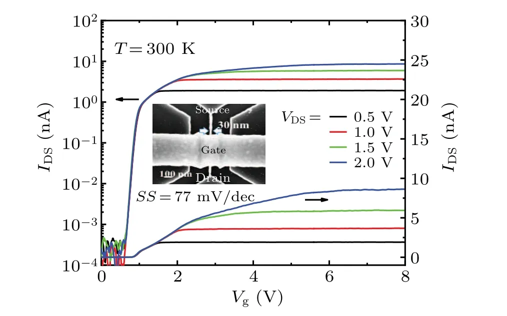
Fig.1. Transfer characteristics of the device at room temperature. The inset is the SEM image of our silicon nanowire after gate formation.
3. Transport spectrum results and discussion
3.1. Low-temperature current characteristics
Figure 2 shows the currentversusgate voltage transfer curves under differentVDSbias voltages(VDS=0.4 V-2.3 V)at a low temperature of 6 K.Below the threshold region,a current peak is observed atVg=1 V for allVDSdrain biases. This current peak is attributed to single-electron tunneling between doping impurities in the channel,which has negligible dependence on the transverse electric field.[18]The current curves of allVDSbias voltages begin to increase dramatically above the threshold voltageVth=2 V,with several similar current steps(seen from the black circle in Fig.2).
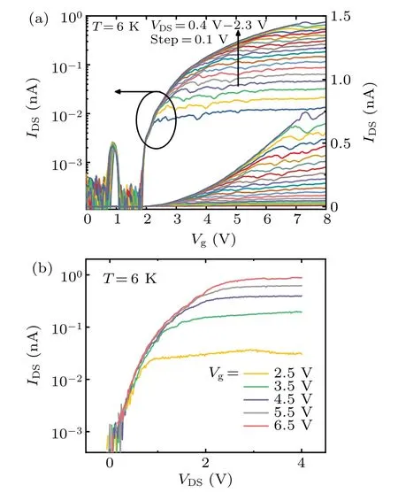
Fig. 2. (a) Transfer characteristic curves under the VDS bias voltages from 0.4 V to 2.3 V at the temperature of 6 K,with curves in log coordinate on the left side and linear coordinate on the right side.(b)The corresponding output curves of the device at the temperature of 6 K.
The transverse electric field is indicated to have less influence on the turn-on position of the device. Interestingly,the conductive currents show obvious fluctuations after the device turning on. The positions of these conductance fluctuations shift to the right withVDSvoltage increasing. Figure 2(b)shows the corresponding output curves with the source/drain voltageVDSchanging from 0 V to 4 V,from which we can see that the transfer curves under the source/drain voltage range(0.4 V-2.3 V)in our main discussion part are absolutely in the safe conductive range of the device. The following part of our paper will focus on the influence of source and drain voltages on these interesting transfer characteristics of our device.
3.2. Threshold characteristics with VDS voltage changing
The threshold position of the device is also related to the position of the edge of the conduction band in the channel.The exact position of the conduction band edge can be obtained from the extended line of the activation energyEawith theVgaxis,where the energy of the electrons in the channel is already enough energy for jumping into the next state that does not need additional activation energy(Ea=0). Figure 3 shows the activation energyEaplots under differentVDSbias voltages from 0.5 V to 2.0 V,with the comparison of the corresponding current curves. The activation energiesEaare extracted from the temperature-dependent conductance of the device at the room-temperature segment(T=250 K-300 K)which are proportionated to exp(-Ea/kBT),wherekBis the Boltzmann constant. Interestingly, the tangent lines of the activation energy(Ea) of all bias voltage settings intersect with the horizontal axis(Vg)at the same position,i.e.,the edge of the conduction band, atVg=2.0 V,[19]indicating that the conduction band edge in the channel is highly dependent on the gate voltage,but has less dependence on the source/drain voltages. Correspondingly, the current curves also start to increase rapidly from this conduction band edge position for all bias voltages,which is exactly the evidence of the position of the threshold voltage(Vth).[20]Generally,the highest Fermi energy position in the channel should reach the Fermi level of the source pool atVg=Vth, where the energy barrier between the source and the channel should diminish,resulting in the device turning on.The transverse electric field introduced from source and drain voltage has quite limited influence on the highest channel energy level close to the source region, as well as the energy barrier between the channel and the source pool, resulting in the independence of theVthposition onVDSvoltage. Besides,we also noticed that the room-temperature activation energy at the highVgconductive region decreases from 176.5 meV to 95.9 meV withVDSbias voltage increasing from 0.5 V to 2.0 V.This is due to that the bias electric field can highly accelerate the thermally activated electrons in the channel,equivalent to thermal temperature on the increase of electron energy.

Fig.3. The current with corresponding activation energy curves for various VDS bias voltages,VDS=0.5 V,1.0 V,1.5 V,2.0 V.
3.3. Transport spectrum beyond the threshold voltage under the influence of VDS
To further explore the mechanism of the current fluctuations in Fig. 2 after the threshold voltage, figure 4 shows the three-dimensional(3D)transconductance(gm)data for variousVgfrom 0 V to 8 V andVDSfrom 0.4 V to 2.3 V at the temperature of 6 K.Clearly,the regular transconductance fluctuations with the stableVgspacing (ΔVg) of 0.81 V, 0.81 V, 0.59 V,0.83 V, 1.07 V, respectively (marked in red arrows in Fig. 4)move linearly to higherVgsection withVDSbias voltage increasing. Let us first focus on these consistent set of fluctuation spacings. The corresponding energy intervals between sub-bands are calculated by[5]

as 91.3 meV,91.3 meV,66.5 meV,93.6 meV,and 120.6 meV,where the oxide layer thicknessdoxinCoxis 10 nm. To study these energy spacings, we calculate the theoretical spacings between discrete sub-bands of silicon nanowire caused by 1D quantum confinement[21]through
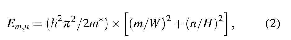
where the effective mass of electronm*is 0.2m0.WandHare the channel width and height, andm,nare quantum numbers in two directions (m,n=1,2,3,...). From this equation,the 1D theoretical energy intervals are calculated as 92.6 meV, 92.6 meV, 61.7 meV, 92.6 meV, 123.5 meV, supposingW=H=8 nm. We can find that the theoretical results are highly consistent with the sub-band energy level spacing observed in the inset of Fig.4. Therefore,we demonstrate that these regular fluctuations are caused by inter-sub-band scattering originated from 1D quantum confinement.
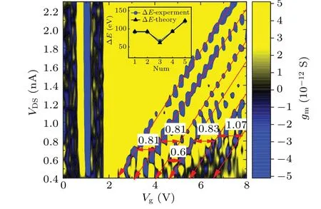
Fig. 4. The transconductance characteristics gm for various Vg from 0 V to 8 V and VDS from 0.4 V to 2.3 V at the temperature of 6 K.The inset shows the sub-bands intervals extracted from the transconductance experiment data and calculated from 1D transport theory.
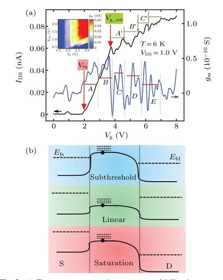
Fig. 5. (a) The current curves at the temperature of 6 K and corresponding transconductance at VDS =1.0 V.The inset shows the transconductance characteristics at the threshold region for various Vg and VDS voltages at the temperature of 6 K.(b)Energy band diagram for the three operation regimes along the nanowire direction.
Figure 5(a)shows the transconductance and corresponding current curves at the temperature of 6 K atVDS=1.0 V.Here we can clearly observe the two sets of fluctuations,with similar spacing as the 1D energy sub-band level intervals. The second set of fluctuations is exactly what we have demonstrated in Fig. 4 as the 1D transform and the positions shift withVDSincreasing. While the first set of transconductance fluctuations from the position aroundVth=2 V do not migrate withVDS, shown from the enlargedgmcharacteristics at the region around threshold voltage in the inset of Fig.5(a).Here, the two sets of conductance fluctuations are related to the sub-band energy levels in the channel (Echannel)intersecting with the Fermi levels of the source (EfS) and drain Fermi energy level(EfD)in turn asVgincreases.[22]The first sub-band in the channel intersects the source Fermi level(EfS=Echannel) at the position ofVth(the conduction band edge),resulting in the current starting to rise rapidly as the first transconductance peak appearing.[23-25]The energy level in the channel and the energy barrier between the source and the channel are strongly controlled by the gate voltage. The transverse electric field induced fromVDScan merely influence the intersection ofEfSandEchannel,therefore,do not influence the threshold voltage. AsVgincrease aboveVth, there come two kinds of situations-the liner region and the saturation region,depending on the relative position ofEchanneland the Femi energy level of the drain poolEfD. Figure 5(b)shows the energy band diagram for the three operation regimes. Here we name“Vg-sat”as the position of gate voltage whereEchannel=EfD.Keeping an unchanged value ofVDS, whenVgis high enough thanVg-sat, the first sub-level in the channel must go below both the drain and source Fermi levels,i.e.,EfS>EfD>Echannel, there comes the linear region. The channel is highly conductive and the current can be expressed as
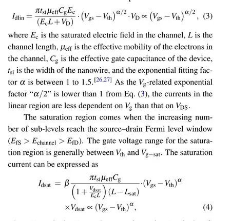
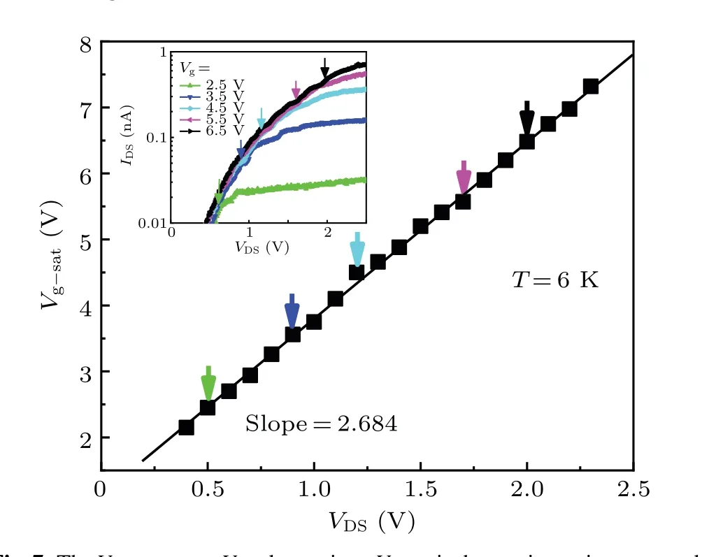
whereVd-satis theVDSat the saturation point,Lsatis the effective channel length. As we mentioned above,theVg-related exponential factorαis larger than 1, which means current at saturation region is highly dependent onVg, which can also be observed in the current curve of Fig. 5(a) in the region ofVth We can use the general formula:y=a(x-b)cfor the currents in both linear and saturation regions according to Eqs.(3)and(4),where the parameterbindicates the threshold voltagesVthwhich should be uniform in both regions,and the exponential fitting factorcin the saturation region isα,and supposed to beα/2 in the linear region. Figure 6(a) shows the fitting results of the two transport regions atVDS=1.0 V. The inset of Fig.6(a)shows the factorsbcorresponding toVthfrom all the transfer characteristics under differentVDSfrom 0.4 V to 2.3 V, which remain quite stable at exactly the position nearVth=2 V. Fig.6. (a)The fitting results of the saturated region and the linear region at the temperature of 6 K under VDS=1.0 V.The inset shows the fitting factors b, which is corresponding to Vth according to the theory. (b)The Vg-related exponential fitting factor c extracted by fitting results from the transfer characteristics of different VDS voltages at the temperature of 6 K.This parameter c in the saturation region is supposed to be twice that in linear region. Figure 6(b) shows theVgrelated exponential coefficientcfor both operation regions, which is twice in the saturation region than that in the linear region as our model. This indicates that in the saturation region, the relatively high transverse electric field makes the current highly limited by gate potential. While in the linear region, the Fermi energy level is under both source and drain Fermi levels, the conductive current in the channel is almost dependent on the energy gap between the drain and the source,which is less influenced by the gate voltage. Another characteristic we should notice from Fig.6(b)is that theVg-related exponential factorcin both regions increases withVDS. The transverse electric field induced fromVDSis supposed to have the role of amplification the gate restriction effect of the channel. Figure 7 shows the positions ofVg-satshift linearly withVDS,with the data extracted from the transfer curves under theVDSfrom 0.4 V to 2.3 V.As discussed above,Vg-satindicates the turning point from the saturation region to the linear region where the energy satisfies the equationEfD=Echannel. The Fermi energy level of the drain regionEfDis mostly dependent on theVDSvoltage and will certainly go down with theVDSvoltage increase. Correspondingly, the turning pointVg-satwillshift to higher gate voltage to upraise the Femi energy level of the channel to rebalance the energy toEfD=Echannelwith theVDSincrease. The inset of Fig. 7 shows the output curves for different gate voltages ofVg=2.5 V, 3.5 V, 4.5 V,5.5 V, 6.5 V at the temperature of 6 K. The turning points of the output currents from the linear region to saturation region are marked as triangles in color, which are exactly consistent with theVg-satpoints fromID-Vgcurves(marked as arrows in color in Fig.7). Fig.7.The Vg-sat versus VDS data points.Vg-sat is the turning point extracted from the transfer characteristics under differentVDS at the temperature of 6 K.The inset shows the output curves of the device at 6 K under different gate voltages of 2.5 V,3.5 V,4.5 V,5.5 V,6.5 V.The triangles point to the turning position from linear region to saturation region. The transconductance curves at room temperature for differentVDSfrom 0.4 V to 2.3 V all exhibit two obvious peaks in Fig.8(a),indicating the position ofVthandVg-satwhich have been discussed above. Besides,the positions of the first peaks(Vth)stay fixed for differentVDS,as the transverse electric field has less influence on the energy barrier between the source and channel to turn on the device. While the second peaks(Vg-sat)shift right withVDSincrease because the higher Femi energy level of the channel required to meet the situation ofEfD=Echannelwhere the transport mode transform from linear mode to saturation mode. We should notice that the regularly transconductance fluctuations almost disappear in contrast to what we have observed before at the temperature of 6 K seen from Fig.8(b). This is because the energy of the electrons at room temperature is high enough to overcome the 1D quantum energy sub-band intervals. Fig.8.(a)The transconductance curves of the device at room temperature under different VDS voltages. (b)The combo chart of the 3D transconductance curves of the device at the temperature of 300 K and 6 K under different VDS voltages. In our work,we studied the influence of source and drain bias voltage on the quantum sub-band transport spectrum in our 10-nm width N-typed junctionless nanowire transistor at the low temperature of 6 K. We observed the single electron tunneling current peaks below the edge of the conducting band which shows the independence ofVDS. We demonstrated that the transverse electric field introduced fromVDShas less influence on the threshold voltage of the device.Above the conduction band edge,the transverse electric field is supposed to have the role of amplifying the gate restriction effect of the channel. The 1D sub-band dominated transport is demonstrated to be modulated byVDSin different ways in the saturation region and the linear region. The turning point from the linear region to the saturation region(Vg-sat)shifts right withVDSincrease because the higher Femi energy level of the channel is required to satisfyEfD=Echannel.We also find that the bias electric field has the effect to accelerate the thermally activated electrons in the channel,equivalent to thermal temperature on the increase of electrons energy. Our work provides a more comprehensive understanding of transport behaviors at nanoscale devices under the influence of changing source/drain bias voltages. Acknowledgement Project supported by the National Key Research and Development Program of China(Grant No.2016YFA0200503).

4. Conclusion
猜你喜歡
瘋狂英語·新讀寫(2022年12期)2022-12-15 13:50:16
考試與評價·七年級版(2021年5期)2021-08-14 21:22:27
——專訪富華國內(nèi)銷售部部長古嘉杰
專用汽車(2020年11期)2020-11-23 09:24:58
——訪富華銷售總監(jiān)張航博士
專用汽車(2020年10期)2020-10-26 01:11:48
Chinese Physics B(2019年10期)2019-11-06 00:46:08
Chinese Physics B(2019年6期)2019-06-18 05:42:38
專用汽車(2016年11期)2017-01-11 02:31:40
專用汽車(2016年5期)2016-03-01 04:14:46
專用汽車(2015年4期)2015-07-08 03:21:04
——走進(jìn)廣東富華重工制造有限公司
專用車與零部件(2015年9期)2015-03-16 01:43:23

- Chinese Physics B的其它文章
- Role of compositional changes on thermal,magnetic,and mechanical properties of Fe–P–C-based amorphous alloys
- Substrate tuned reconstructed polymerization of naphthalocyanine on Ag(110)
- Anti-PT-symmetric Kerr gyroscope
- Information flow between stock markets:A Koopman decomposition approach
- Cascading failures of overload behaviors using a new coupled network model between edges
- High efficiency ETM-free perovskite cell composed of CuSCN and increasing gradient CH3NH3PbI3