
Resistive switching memory for high density storage and computing*
2021-05-24 02:23:04XiaoXinXu許曉欣QingLuo羅慶TianChengGong龔天成HangBingLv呂杭炳QiLiu劉琦andMingLiu劉明
Chinese Physics B 2021年5期
Xiao-Xin Xu(許曉欣), Qing Luo(羅慶), Tian-Cheng Gong(龔天成), Hang-Bing Lv(呂杭炳),Qi Liu(劉琦), and Ming Liu(劉明)
Key Laboratory of Microelectronics Devices and Integrated Technology,Institute of Microelectronics of the Chinese Academy of Sciences,Beijing 100029,China
Keywords: resistive switching memory(RRAM),three-dimensional(3D)integration,reliability,computing
1. Introduction
Memory is one of the basic elements in semiconductor integrated circuit and has an increasing demand on density,power consumption, and performance. The current mainstream in nonvolatile memory market is the flash memory,whose density is predicted to be multiplied in every two or three years by Moore’s law.[1]The conventional approach for increasing the density is to shrink the pitch size by advanced manufacturing process. However, as the cell size proceeds down to 10 nm, the planer two-dimensional (2D) structure is facing serious challenges in terms of physical limitation of device structure, coupling of line-to-line, etc.[2,3]Besides, the benefit brought by the increased density becomes insufficient to compensate the growing cost of advanced fabrication process. In view of this condition, both academic and industrial communities turn their sight to the vertical integration of memory array with so called BICS (bit cost scaling), TCAT(terabit-cell-array transistor), or VSAT (vertical stacked array transistor) structures.[3–5]The vertical three-dimensional(3D) integration is becoming a key approach to realize high density with tera-bit per cm2. Among the various new concept emerging non-volatile memories, the resistive switching random access memory (RRAM) owing to its simple structure, good compatibility with complementary metal–oxide–semiconductor transistor (CMOS) process, ease of stacking with the back end of line(BEOL),has received enormous attention from the research community.[6–13]According to the international technology roadmap of semiconductor (ITRS)2013,[14]the RRAM was thought as a new technology being worthy of additional focus to accelerate the commercialization process.
The RRAM array architecture can be divided into two categories, passive array or active array. In passive array, the memory cells are located at the cross-point of perpendicularly placed parallel wordlines (WLs) and bitlines (BLs). In 2D planer structure, it can achieve the smallest cell size of 4F2(F is the feature size). Because of the independence of the processes of the front-end-of-line (FEOL), the passive crossbar array can be readily stacked along with the process of the BEOL. Given an N layered crossbar array, the cell size per bit will be as small as 4F2/N. This highly compact integration manner owns a promising prospect for high density data storage. In contrast, the active array, with a 1T1R (one transistor one resistor) structure as its general form, can perfectly insulate the accessed cell from neighboring cells by a transistor, which also provides compliance to avoid overprogramming. Because of its logic based integration manner,the 1T1R structure becomes a rational choice for embedded application.[15–20]However, the transistor consumes silicon area and is incapable of multi-layer stack, making the 1T1R structure difficult for 3D integration. There are also some reports combining the passive and active integrations together by adopting such a structure named 1TxR with a purpose of better performance and higher density.[21,22]In 1TxR structure,each transistor drives a vertically stacked ninny crossbar array. This architecture can balance the strict requirement of high nonlinearity in passive array and difficulty of 3D integration in active array. Considering the design of 1TxR structure overlapped with the passive array in terms of nonlinearity and leakage current,this structure will not be discussed extensively in this paper.
The major task of designing a 3D passive array is to achieve a low cost, highly compact memory array and to operate each cell in array correctly without disturbing the neighbors. The fabrication cost mostly depends on the array architecture, e.g., stacked array or vertical array. The later one is also called vertical RRAM (VRRAM), with less lithography steps for patterning and thus lower cost. There are various challenges in 3D passive array designing, such as the sneaking current,disturbance,IR drop,thermal coupling,etc,which greatly retard the progress towards commercialization.Apart from data storage, the passive network also has other potential applications, such as neuromorphic computing,[23]3D CMOS/molecular circuits(CMOL),[24]etc., with promising prospect of low cost and high energy efficiency. In this review article,we will firstly address the associative problems in passive array and 3D architectures(Section 2),and then review the states of the art of various selector devices and selfselective cells (Section 3). Key parameters that influence the device nonlinearity and current density are discussed based on the corresponding working principles. Section 4 addresses the reliability issues in 3D array such as uniformity, endurance,retention,disturbance,etc.,and Section 5 discusses the issues of scaling and thermal crosstalk in 3D memory array.Applications of 3D RRAM beyond storage,such neuromorphic computing and CMOL circuit are discussed in Section 6. Summary,discussions,and outlooks are given in the final.
2. Associative problems in passive array and 3D architectures
Passive storage arrays can achieve the highest storage density at a very low cost. However,the leakage current problem in passive arrays could lead to problems of reading errors and disturbance of resistance state in partly selected cells. In addition,the IR drop and thermal coupling become more and more serous as the array size increases.
2.1. Sneaking current problem
The sneaking current path is a fundamental problem commonly existing in 2D or 3D cross-bar array,[25–30]as shown in Fig.1. In the V scheme, the voltage with magnitude V is applied only to the selected word line, while all the unselected word and bit lines are floating. If the R2, R3, and R4 are at low resistance state, the readout state of the selected R1 will always be low resistance state(LRS)whatever the state of R1 is. The sneak current path consists of two forward biased halfselected cells and a reverse-biased cell. Here,the forward and reverse bias directions are defined as being identical and opposite to the bias at the selected cell. Hence,there are two ideas to solve the leakage problem.Firstly,connecting a diode selector can impede the sneak currents by limiting the current flow through the reverse-biased cell R2. In such a way,the sneaking current from the undesignated cell could be suppressed by adopting a bias scheme of ?V method,i.e.,the selected cell is biased by V and the unselected cells is bias by ?V or 0. However,the diode selector has some inherent limitations,such as area dependence of driving current and inconsistency with the bipolar device.[31–33]Secondly, decreasing the current of the forward-biased cells of R3 and R4 at the low-voltage region by constructing a threshold switch in LRS.Given this,the selector device with symmetrical(or nearly symmetrical)highly nonlinear I–V relationship was put forwards.[34]The nonlinearity(η),defined as the ratio of I@Vread/I@(Vread/2)is helpful to diminish the sneak current from undesignated cells by using V/2 bias scheme. Besides introducing separate selector device, developing self-selective cell (SSC), such as build-in nonlinear device,complimentary switching device,etc,is also a feasible way to solve the sneaking current issue. As will be discussed later, the SSC device has special meaning for the VRRAM designing.
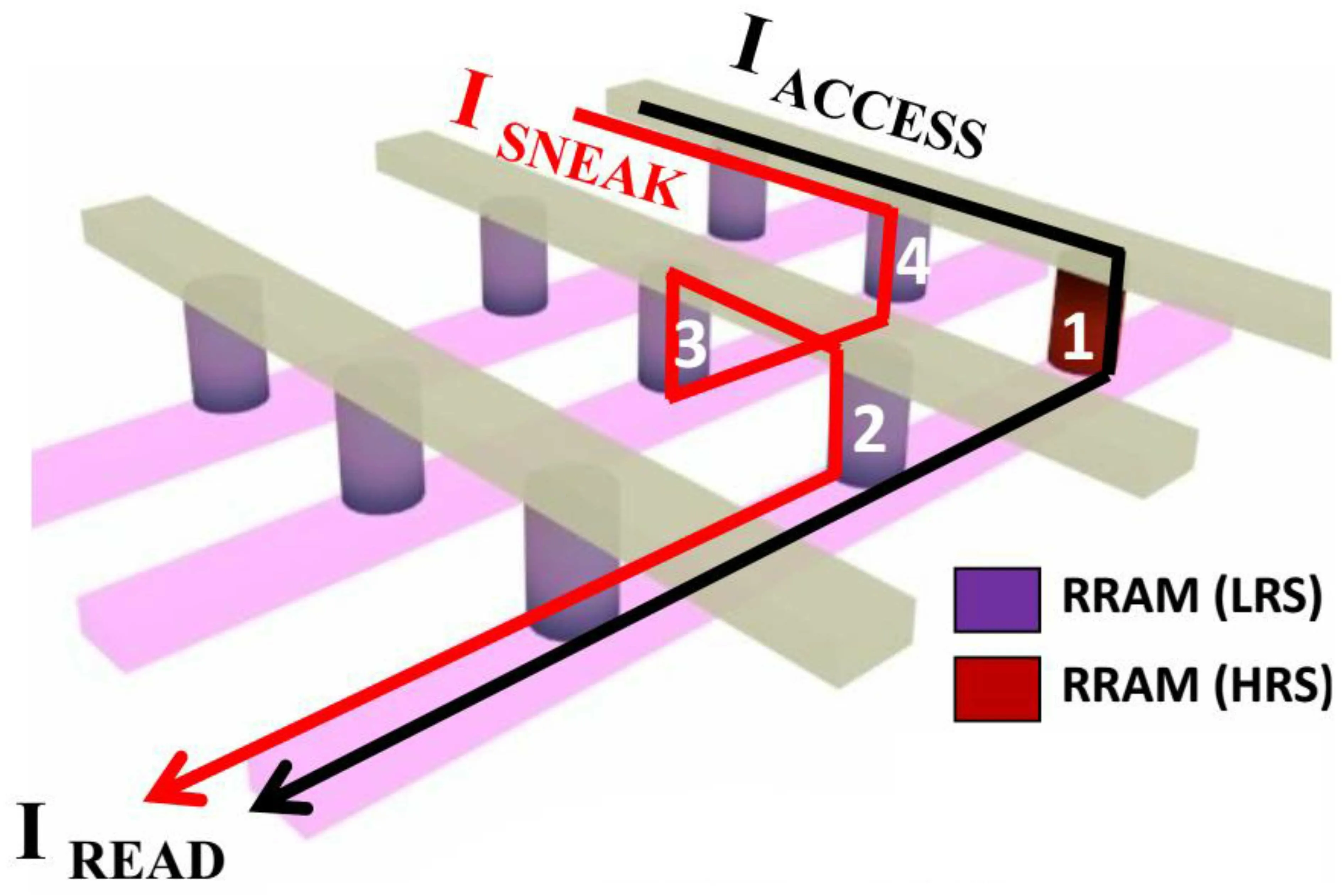
Fig.1. A schematic diagram of the typical cross-bar showing the read disturbance problem by the presence of sneak current.
2.2. Disturbance issue
The disturbance mainly occurs in the devices which locate in partly selected rows or columns, depending on different bias schemes. In a passive array, the V/2 bias scheme is widely adopted in order to reduce the interference of unselected cells. In this scheme, the half-selected cells suffer from consecutive sub-switching voltage and bear the risk of the change of resistance states.This is usually called programming disturb. The disturbance issues are much more complicated in an array. In the cross-point RRAM arrays, because of waveform degradation caused by the parasitic resistance and capacitance of the bit-lines and word-lines,voltage signals larger than the critical switching voltage are usually applied in order to ensure the correct programming for the farthest cell.In this case, half-selected cells nearer to the voltage supply will suffer from larger voltage stresses than V/2 and serious disturb issues during the programming operation. The adoption of nonlinear selector could moderate the disturbance issue greatly,because most of the voltage will be dropped on the selector device at low voltage region.
2.3. IR drop issue
The IR drop issue is related with the voltage drop on the WLs or BLs. According to the reported data, the resistance of a metal line is exponentially dependent on its size in nm scale.[38]This makes the resistance of metal line ineligible as compared with the resistance of memory cell. A large potential difference is applied across selected cells by driving the corresponding wires to high voltages. Some part of the applied voltage could be dropped on the metal lines and the unselected cells (Fig. 2), making the voltage applied on the cell lower than expected. The total voltage drop across any selected nonvolatile memory (NVM) device must be sure to switch the device, despite the additional voltage drop in its own access device and in the wiring. The worst case happens in the device located at the farthest corner.
The IR drop issue will not only deteriorate the read/write disturbance, but also increase the sneak current, in the case of the leakage of the selector highly dependent on voltage bias.[39]Increasing the device nonlinearity could be helpful to improve the capability of voltage delivery. Comparison between the voltage distributions along the WL in the arrays with linear and nonlinear devices shows that higher nonlinearity could result in less degradation of delivering voltage.[40]Together with the nonlinearity and on/off ratio,the metal line resistance becomes the main factors on determining the maximum reachable array size.
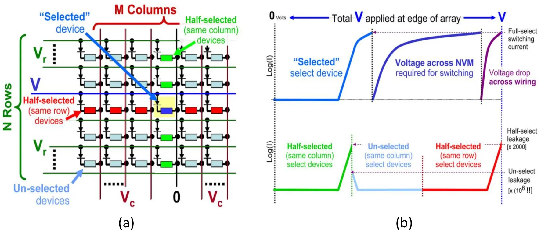
Fig.2. (a)In a cross-point array of NVM devices,three other sets of NVM/access devices would be affected when selecting one NVM/access device pairs, including the half-selected cells and unselected cells, as well as the wires. (b)The total voltage drop across any selected NVM device must be sure to switch the device, despite the additional voltage drop in its own access device and in the wiring. However, that same applied voltage must not lead to excessive leakage in either the half-selected or unselected devices.Reproduced with permission from Ref.[40].
2.4. Thermal coupling
The thermal coupling is related with the resistance state changes in the neighbor cells resulting from the high temperature generated during programming. Despite the resistive switching mechanism is related with several aspects,there is a common sense that Joule heating or thermal effect plays an important role in it,regardless the switching type.[43–47]Temperature as high as hundreds of degrees could be generated inside the device during programming. The large amount of Joule heat will cause the resistance degradation in adjacent memory cells of the RRAM crossbar array. On one hand, the thermal dissipation of a programmed cell depends on the thermal conductivity of its surrounding material, such as insulating layer and metal line. One the other hand, it is also influenced by the structural factors,such as 3D architecture and selector device. Higher thermal conductivities of the insulating material,a larger LRS resistance, and a faster operational speed were found to effectively reduce the thermal disturbances in 3D one selector one resistor (1S1R) RRAM crossbar arrays. Since it is difficult to directly monitor the temperature profile produced inside the array during programming,the development of analytical model is helpful to analyze the thermal issue and figure out a guideline for structure designing.
2.5. The 3D architecture
The 3D RRAM is considered as one of the strongest contenders for NAND due to its aggressive scalability. Two typical 3D architectures, the 3D vertical RRAM (VRRAM) architecture and 3D horizontal RRAM (HRRAM) architecture,have been proposed.The former one is deriving from 3D vertical NAND architecture and process,while the latter is realized by stacking planar cross-point arrays layer by layer.
The HRRAM is believed to have higher lithograph cost since the numbers of lithography masks and process steps are dependent on the number of stack layers. In comparison, the VRRAM is the most economical as the channel hole is onetime implemented. However,the 3D VRRAM is not expected to scale aggressively with the advanced technology since the reliability is relatively dependent on the diameter of the channel hole. Besides,it puts forwards higher requirements on material etching and deposition process,adding the cost of fabrication. The HRRAM is considered free from the scaling limitation due to the simple fabrication process. Single cell lateral scalability below 10 nm and vertical scalability below 5 nm have already been demonstrated,thus very small cell area and ultra-high memory density can be achieved in 3D HRRAM.
3. Selector devices and self-selective cells
3.1. Nonlinear selector devices
An ideal selector should have several requirements for application in stacked cross bar array. In each selected cell, the selector should be capable of supplying high current to meet the needs of programming and erasing the memory element in series,typically on the order of several MA/cm.[2,29,36,39,40]The aggregate leakage through all the unselected cells should be as low as possible, since the number of unselected cells is much larger than that of the selected cells,thus dominating the power consumption of the entire array. The first two points mentioned above(high on-state current and low off-state leakage)means that the selectors should have a highly nonlinearity.To satisfy the needs of the RRAM device which is operated in bipolar mode, the selector should also be capable of bidirectional operation. Furthermore, since the selector is used for stacked cross bar array,it should be fabricated by BEOL compatible process. The property of the selector should not be a limitation of RRAM performance,including switching speed,endurance, variability, and so on. All the requirements listed above are the targets of the selector. Various selector devices will be discussed in following in terms of their strengths and weaknesses.
Selectors with different structures and different theories have been reported in the past few years. Two-terminal NPN diodes have been proposed as selector.[53,58–61]Srinivasan et al. obtained a maximum ON/OFF ratio (>106)and high ON-state current density (>1 MA/cm2),[53]as shown in Fig. 3(a). However, the epitaxial growth process and the crystalline Si template require high temperature (~700°C) process. Such a device is not BEOLcompatible and incapable of stacking above the Si substrate.This condition has motivated research into non-Si-based selector with a low temperature process. Non-Si-based selectors can be divided into several groups according to their mechanisms, such as oxide diodes, threshold switch, oxide tunnel barrier, and mixed-ionic-electronic-conduction. Several groups have studied diodes made from semiconducting oxide hetero-junctions[48,62,63]and two-terminal metal–insulator–metal (MIM) structures.[54,64]In these works, the most considerable one was reported by Huang et al., with Ni/TiO2/Ni structure,having an ON/OFF ratio of ~4700,[54]as show in Fig. 3(b). A small 8×8 crosspoint 1S-1R array was demonstrated by implementing Ni/TiO2/Ni selector with bipolar RRAM. This selector device has advantages of high temperature(125°C)operation and being capable of scaling,however,the endurance and disturbance were not mentioned.
The threshold switching devices with high selectivity and low off-current are essential to suppress the sneak current from the neighboring cells which can lead to failure of write and read operations.It turns on from an initial low conducting state to a highly conducting state as soon as a threshold voltage or current is applied. Various types of threshold switches have been proposed in literatures.[55,56,65]As shown in Fig. 3(c),in a nanoscale VO2device, the current through it increases suddenly at 0.35 V as the conductivity of VO2changes from an insulating state to a metallic one.[55]If the voltage is reduced below 0.2 V,the current decreases suddenly as the VO2returns to its initial insulating state. Furthermore, this device shows very fast response(<20 ns),stable and uniform switching and holding voltages.However,for practical application at high temperatures up to 85°C,it fails because of the low transition temperature (~67°C). Another metal insulator transition (MIT) selector (Pt/NbO2/Pt) with higher transition temperature shows excellent thermal stability up to 160°C, and exhibits well-behaved and repeatable hysteretic I–V characteristics over 1000 switching cycles(Fig.3(d)).[56]However,the leakage of this structure was high and only limited nonlinearity was achieved. Figure 3(e)shows the typical I–V curve of a threshold vacuum switch(TVS).This device exhibits high current density (>100 MA/cm2), high selectivity of >105, and good endurance of over 108cycles using 100 ns programming pulses. However, array level demonstration was not reported and the variation was an issue of big deal considering that the tunneling current is highly dependent on the ultranarrow vacuum gaps. Oxide tunnel barrier is an attractive approach for achieving strongly nonlinear I–V characteristics. Tunnel barriers can be formed by high-k materials(HfO2, ZrO2, and TiO2).[34,57]Luo et al.[34]reported TaOx-based selector with trapezoidal band structure (Ru/TaOx/TaOy/W), as shown in Fig. 3(f). Low off-state current (~10 pA) and large nonlinearity (~5×10⁴) have been achieved. Excellent uniformity was achieved during 103successive DC cycles. No disturbance was observed under read and half-read conditions during 1010pulse endurance test. This selector was fabricated in 1 kb crossbar array and the integrated 1S1R device showed high nonlinearity in low resistance state(LRS).
Copper-containing mixed ionic-electronic conduction (MIEC) materials have been proposed for 3D-ready selector.[66–69]As demonstrated in the work from IBM research group, MIEC-based selectors offer high nonlinearity(107), ultralow leakage (<10 pA), high voltage margin Vm,and excellent turn-on speed (<50) (Fig. 4(a)). MIEC materials contain a lot of mobile copper ions, which can move readily under an electrical field. At low bias, the Schottky barrier at the interfaces between MIEC and electrode,strongly suppressing the hole conduction, leads to the low leakage.As the bias increases, copper ions move toward the negative electrode, modulating the interfaces and leading to an exponentially increase in electronic current. Figure 4(b) shows the endurance of the MIEC-based device. As the compliance current increased,the endurance of this device was degraded.Good endurance as high as 106was achieved in the case of high operating current (~150 μA). Excellent uniformity was observed according to the cumulative distribution functions(CDFs)of the I–V characteristics in an array(Fig.4(c)).MIEC based access device could maintain low-leakage over hours of exposure, both in a deep (±230 mV) and shallow un-select (±350 mV) condition (Fig. 4(d)). To demonstrate access characteristics of MIEC devices,a PCM+MIEC device was formed. Implementation of MIEC selector into phase change memory crossbar array in a form of 1S1R structure was successfully demonstrated. As shown in Fig. 4(e), more than 106switching cycles with RESET currents >200μA and 5 μs-long SET pulses (~90 μA), were achieved, indicating that the MIEC device has a hopeful prospect for selector use.Further improvements would include a higher endurance at high current and increase the voltage margin so as to enable large arrays for NVM requiring more than 1.5 V switching voltage.
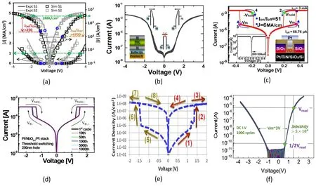
Fig. 3. (a) Current density vs. voltage plots for two NPN structures with different doping profiles. (b) Bidirectional exponential current–voltage curves measured on the devices with the structure of Ni/TiO2/Ni. (c)I–V characteristics of threshold selector of the Pt/VO2/Pt device.(d)I–V characteristics of nanoscale niobium dioxide device structured as Pt/NbO2/Pt. (e)I–V characteristics of TVS selector. Arrows(1)→(8)represent the measurement sequence. TVS volatile switching behavior provides high current density and selectivity. (f)Typical I–V switching characteristics of a tunnel barriers selector(Pt/TaOx/TiO2/TaOx/Pt). Reproduced with permission from Refs.[34,53–57].
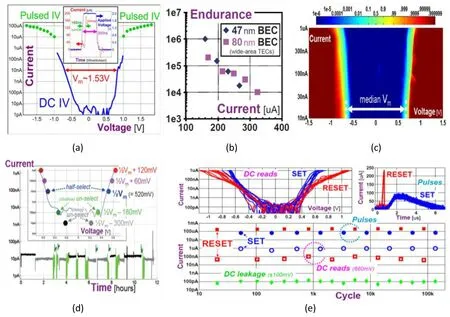
Fig.4. (a)Typical I–V curves of MIEC selector showing >107 nonlinearity and <50 ns turn-on switching(insert). (b)MIEC-based selector endurance depends on current,but is independent of bottom electrode contact CD.(c)The I–V results with tight distributions across a 512×1024 array of integrated MIEC access devices. (d) MIEC selectors exhibit highly immunity in a deep (±230 mV) or shallow un-select(±350 mV)condition. (e)The PCM and MIEC device-pair shows excellent endurance up to 100k cycles. Reproduced with permission from Refs.[66–69].
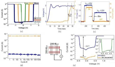
Fig.5. (a)The I–V characteristics of FAST selectors with different thicknesses of the active layer. (b)Off-to-on transition time is about 5 ns(tester limited)for the selector. (c)The selector quickly relaxes to the off state in less than 50 ns. (d)The selectors can be reliably cycled over 100M cycles while maintaining >106 on/off ratio (test limited). (e) The 1-bit (100 nm×100 nm) leakage current can be projected through entire 40 kb devices. Inset: Typical I–V of a selector on the same wafer. Reproduced with permission from Ref.[70].
Field-assisted super linear threshold(FAST)selector was reported by Jo et al.[70]Excellent selector performance was presented such as selectivity of 1010,sub-50 ns operation,and 100M endurance. Figure 5(a) is the typical I–V curves of a FAST selector. The threshold voltage(Vth)of the selector can be turned by controlling the thickness of the active layer. The turn-on speed is less than 50 ns under applied voltage aboveVthand the on-to-off transition time is less than 5 ns (Fig. 5(b)).The selector can recover quickly to the off-state when the voltage is removed, with a recovery time <50 ns(Fig.5(c)).Figure 5(d) shows that the device can reliably switch over 100M cycles. To extract the intrinsic leakage current of the FAST selector, the leakage current through an entire 40 kb selector array was measured(Fig. 5(e)). The extracted selectivity is extrapolated to be as high as 1010(@100 nm device).The FAST selector almost meets all the requirements that an ideal selector should have. However,the intrinsic mechanism and the compatibility with CMOS process have not been revealed yet. The similar threshold switching selector based on Cu:HfO2was proposed by Luo,[71]which shows high nonlinearity and ultra-low off-state. The threshold switching behavior is originated from the spontaneously rupture of the unstable conductive filament. Zhao et al.[72]proposed a high driving current selector by utilizing graphene defect engineering in the structure of Pt/SiO2/graphene/Ag. This selector exhibited excellent bidirectional selectivity as high as 5×10⁸under high complicate current and demonstrated the ability to suppress the crosstalk issue in large memory arrays.
3.2. Self-selective devices
The 3D vertical RRAM provides a cost-effective approach for high density integration. However, unlike 3D stacked crossbar array, individual selector is not allowed in VRRAM. Developing high performance self-selective cell(SSC) is the most critical issue for the integration of vertical RRAM.Some attractive device configurations have been proposed to realize self-selective cell,such as build-in nonlinearity device,self-rectifying device,and complementary resistive switching device.
Park et al. reported a resistive switching memory with build-in nonlinearity by inserting a thin barrier layer between oxide and electrodes.[50,75]The device exhibited a nonlinearity about 17 under low compliance current of 1μA(Fig.6(a))and could be repetitively switched between LRS and HRS for more than 107cycles with 1μs voltage pulses,maintaining an on/off ratio about 100. Figure 6(b) shows the non-linear I–V characteristics of the Ti/HfOx/TiOx/Pt RRAM device with higher compliance current ~50 μA and 20 μA. Lightly increased nonlinearity about 23 was observed. However, it is still not large enough to prevent the leakage of the unselected cell in a large crossbar array. Son et al. reported a hybrid memory device which combined metal–insulator transition and memory device together by controlling oxygen concentration in vanadium oxide film.[73]Vanadium oxide film with various intermediate oxygen content showed hybrid characteristics,with nonstoichiometric V2O5?xfilm showing typical resistive memory switching behavior and stoichiometric VO2film exhibiting typical MIT behavior. As shown in Fig.6(c),this device exhibited both threshold switching and bipolar memory switching behavior and had nonlinearity about 80. Similar to vanadium oxide but offering a higher transition temperature,niobium oxide exhibits both memory and selection properties for intermediate oxygen concentrations.[74]Figure 6(d)shows the typical I–V curve of W/NbOx/Pt memory device.The LRS of the memory device offers a nonlinearity of 102.Without additional selector device,1 kb cross-point array based on the hybrid memory device with successful SET/RESET operation up to 106cycles was demonstrated.However,all the devices mentioned above were not integrated on 3D V-RRAM and further improvements are still needed for application of large-scale array.
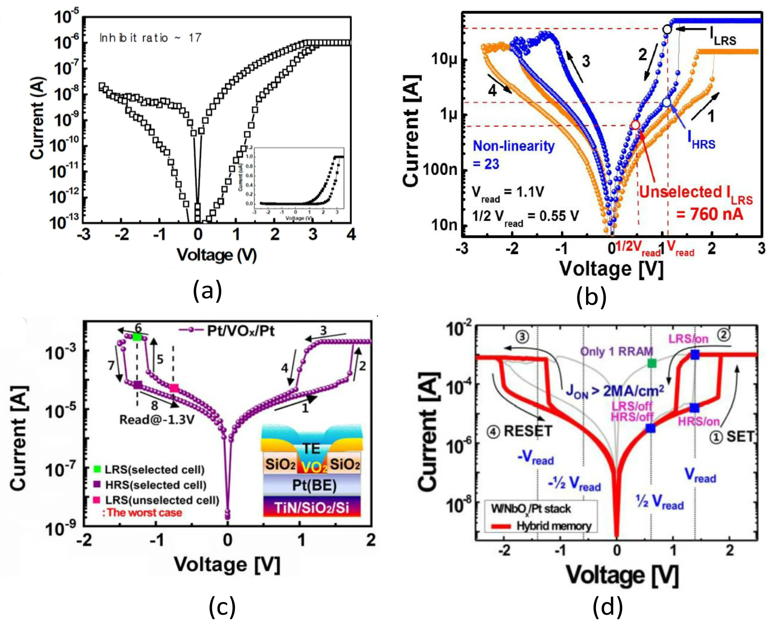
Fig.6. (a)The I–V curve of the structure of TE/TMO/BE.(b)Typical I–V curves of the self-selective RRAM(Ti/HfOx/TiOx/Pt). (c)I–V curve of the hybrid-type Pt/VOx/Pt device. Inset: Structure of the nanoscale device. (d)I–V characteristics of hybrid(W/NbOx/Pt)memory device.Reproduced with permission from Refs.[73–75].
Luo et al.[76]successfully demonstrated a self-selective device with extremely high nonlinearity of 1000 and ultra-low leakage current (0.1 pA). The hybrid devices combine HfO2layer as the switching layer and mixed ionic and electron conductor(MIEC)layer as the selective layer. Based on this SNR device, a four-layer 8×32 VRRAM 3D array was successfully demonstrated. Figure 7(a) is the schematic of 4-layer VRRAM and SEM images of in-line checks. After multiple TiN(60 nm)/SiO2(100 nm) layers deposited respectively,patterning and one-step etching were applied to form stacked wordlines(WL).HfO2/CuGeS bilayer and top electrode were deposited on the sidewall,followed by liftoff process to form bitlines(BL).Figure 7(b)is the TEM image and EDX line scan of the device. Well-distinguishable layers with clearly identified interface could be observed. Figure 7(c)shows the typical I–V characteristics of HfO2/CuGeS bilayer device. The halfselect leakage as low as 0.1 pA and nonlinearity as high as 103were achieved. In addition,the operation current below nA is beneficial to realize low power consumption and high-density storage. As shown in the insert of Fig.7(c),the programming voltage of the SSC can be modulated by the thickness of the CuGeS layer. Figure 7(d)is the typical I–V sweeping curves of the cells in 4-layer VRRAM array. Each layer device exhibits stable and uniform self-selective memory characteristics. Other excellent characteristics such as high endurance(>107)and robust read/write disturbance immunity were also presented.
The self-rectifying characteristics within the individual cell is another approach to suppress the sneak current in high density array in 3D VRRAM. The I–V characteristics of the self-rectifying is similar as the one diode one resistor(1D1R)structure, showing the obvious rectification in low-resistance state. The rectification is originated from the Schottky barrier created neither at the interface of electrode and switching layer or at the conjunction of filament and buffer layer. Initially, semiconducting electrodes such as n-Si or n-Ge were usually used,[73,77]with corresponding I–V curves shown in Fig.8(a). Although the rectifying ratio for these devices was reported as high as 106, the Si or Ge based self-rectifying device has inherent drawbacks, due to the high processing temperature, making them incapable to be stacked layer by layer in BEOL process.[78]In order to achieve a stackable self-rectifying device, semiconducting buffer layer was introduced between the metal electrode and switching layer, e.g,a-Si/WOx/Pt structure proposed by Lv et al.[79]In this device,the semiconducting material (a-Si) acts as the role of c-Si or c-Ge, while having lower processing temperature and stackable capability (Fig. 8(c)). However, the rectifying ratio was not satisfactory because of the large amount of interface traps(Fig. 8(d)). Yoon[80]proposed a two-layered device, where a Pt/Ta2O5/HfO2?x/TiN with high uniform, forming free,and self-rectifying characteristics was proposed (Fig. 8(e)).The working principle of this device is that the HfOxlayer works as resistive switching layer by electron trapping and de-trapping process,while the other dielectric layer Ta2O5remains intact during the switching cycles and creates a high Schottky barrier with the metal electrode(such as Pt)of high work function. The high uniformity takes the advantage of electronic switching mechanism, by avoiding uncontrolled ions migration. The most recent progress achieved on selfrectifying device came from Li’s work,[81]a fully foundrycompatible, all-silicon-based and self-rectifying memristor with a p-Si/SiO2/n-Si structure was demonstrated. The device exhibits 105rectifying ratio,104on/off ratio,and excellent retention at 300°C. The 3D crossbar arrays up to five layers were further build.
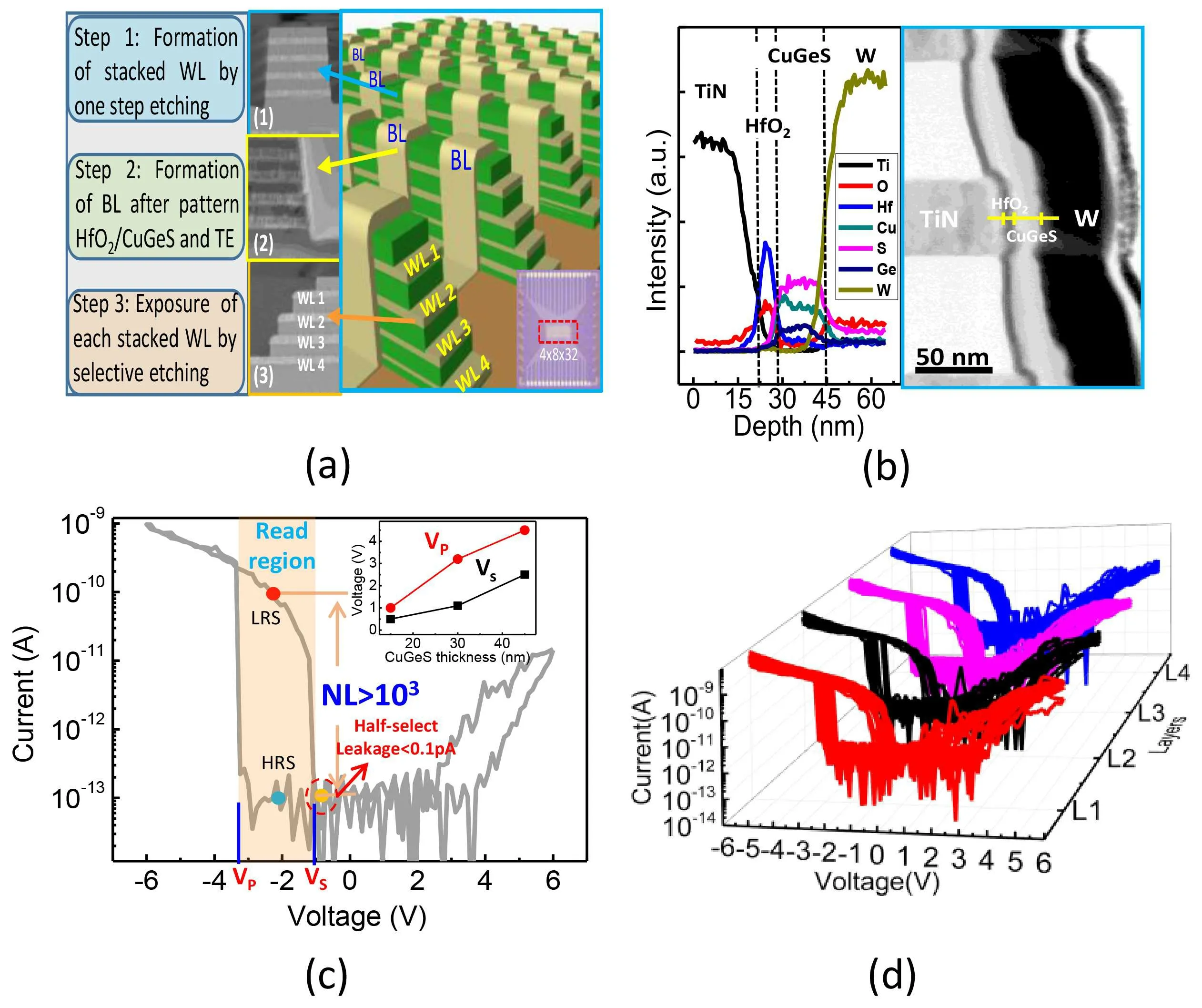
Fig. 7. (a) The process integration of 4-layer 3D V-RRAM. (b) TEM image and EDX line scan over the cross-section of the SSC device(TiN/HfO2/CuGeS/W). (c) Typical I–V curve of the bilayer SSC. Insert: The dependence of the programming voltage (VP) and selective voltage(VS)on the thickness of CuGeS.(d)The devices exhibit stable and uniform I–V curves in the 4-layer 8×32 arrays. Reproduced with permission from Ref.[76].
The complementary resistive switching (CRS) device consists of two back-to-back-connected bipolar resistive switches. The concept of CRS was firstly proposed by Waser and co-workers,[80–82]its schematic and typical I–V curve are depicted in Figs.9(a)and 9(b),respectively,based on conductive bridging memories(CBRAM)as the switching elements.The anti-series connected pair exhibited four possible combinations of HRS and LRS, as shown in Fig. 9(c). Beginning with an original HRS/HRS state,the HRS/LRS can be defined as the state‘0’and LRS/HRS as the state‘1’. The read operation was performed under a read voltage between Vth1and Vth2.The leakage at half read voltage was determined by HRS,thus greatly suppressing the sneak current. As the stored information was‘0’,the read voltage had no influence on both top and bottom cells. However,as the stored information was‘1’,the read operation of the CRS cell was destructive, because the read voltage higher than Vth1could trigger the bottom cell into LRS. In this case, the read-out current was high (On state),given both top and bottom cells being at LRS. After reading,a write-back process was required to return the CRS device back to state‘1’. This partly destructive read out characteristics could be one of the inherent drawbacks of CRS device,which could increase the complexity of peripheral circuitry
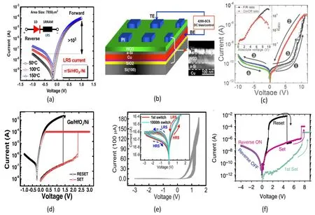
Fig.8.(a)The I–V curves of n-Si/HfOx/Ni device.(b)Schematic of Cu/a-Si/WO3/Pt device.(c)I–V curves of Cu/a-Si/WO3/Pt device.(d)I–V curves of Ge/HfOx/Ni device. (e)I–V curves of TaOx/HfO2 bilayer self-rectifying device. Insert: The rectifying and On/Off ratio at different applied voltages. (f)Electrical behavior of p-Si/SiO2/n-Si self-rectifying device. The ON/OFF ratio was higher than 104 and rectifying ratio~105 when bias voltage was larger than ?1.5 V.Reproduced with permission from Refs.[77,79,81,82].
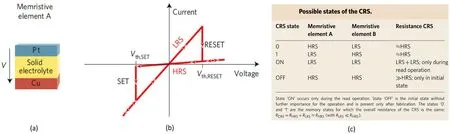
Fig.9. (a)Schematic of a CRS device with back-to-back connected two CBRAM cells. (b)Typical I–V curve of CRS device. (c)Two stored data states amongst the four possible combinations of individual device states. Reprinted with permission from Ref.[80].
4. Reliability issues of RRAM
High-density integration of RRAM cells is the precondition for its future commercialization. Since the yield,density,and operating property of the memory chip are limited by the performance characteristics of the worst cell,the intrinsic uniformity and reliability characteristics of memory devices become critically important. For peripheral circuitry techniques used in the memory hierarchy,a high homogeneity of the devices is critical.The endurance is an important reliability characteristic because higher endurance broadens the application area where frequent read/write operation is required. Retendesigning. In contrast to the CRS devices with connecting metal–dielectrics–metal stack in series, the one proposed by Nardi et al. only contained single layer structure.[81]By selectively forming the filament at the top or bottom interface,bipolar CRS behavior was successfully demonstrated. Similar phenomenon was also reported in other literatures.[82–86]tion(stability)is crucial for the nonvolatile memory operation and restricts the intended application of RRAM, such as in code storage,space,high temperature application,and FPGA.The potential scalability to nanometer regime of RRAM devices plays a key role in competitive advantage compared with the traditional Flash memory.Without critical scaling technology, multi-level operation is a desirable capability for highdensity memory application. Table 1 summarizes the performance of the RRAM device in 3D architecture reported in recent years.In this section,we will discuss these characteristics of RRAM in terms of 3D architecture.
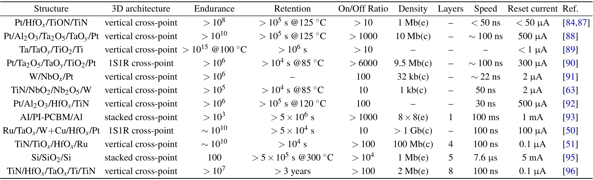
Table 1. The performance of the RRAM device in 3D architecture reported in recent years.
4.1. Uniformity
The significant parameter fluctuation is a major barrier to the practical application of RRAM. The fluctuant parameters of RRAM include the operation voltages and the resistances of HRS and LRS,which common exist not only in cycle to cycle,but also in device to device.[87–90]Since the large device-to-device variation of the resistances or switching voltages may cause the read/write failure, the uniformity of the switching parameters is more crucial for the array operation demonstration. The uniformity issue of RRAM is originated from the stochastic oxygen vacancies/ metal ions motion.[8]Chen[91]demonstrated the 3D cross-point architecture with stacking multi-layer vertical RRAM. They showed the consistent switching characteristics among the cells in different layers. The LRS and HRS are about 100 k? and 1M?, respectively, with the HRS/LRS ratio around 10. The set/reset voltages of the samples in three layers almost coincide with each other,indicating high uniformity of the 3D memory cells.
In filament-type RRAM cells, the oxygen vacancies/metal ions deposition and dissolution are commonly utilized to delimit the resistive switching operation.[8]During the set process, the intrinsic erratic filament (e.g., size/ number and location) causes the fluctuation of RLRSand the reset voltage. Meanwhile, the indeterminate tunneling gap formed in the RESET process is responsible for the variation of RHRSand subsequent SET voltage. It is also found that the LRS/HRS variations are influenced by the oxygen vacancies/metal ions concentration inside the filament region/tunneling gap region.[92]The unstable switching parameters of RRAM cells must be solved before practical application. Many efforts have been implemented for this issue,such as electrode/oxide interface engineering, location of conductive filament paths,and utilizing optimized operation method.[84,87,93,96–99]
It is well known that embedding appropriate buffer layers in electrode/oxide interface is an effective approach to optimize the RRAM performance.The additional layer could play a role of an oxygen reservoir. By embedding the Al layers,the uniformity of switching parameters of the Pt/AlOy/HfOx/TiN based vertical RRAM devices is remarkably improved compared with Pt/HfOx/TiN devices.[100]Figures 10(a)–10(c)show the resistance and switching voltage distribution in temporal and spatial scale. Both the cycle-to-cycle and device-todevice uniformity are improved with AlOyincorporation. The improvement is attributed to that the Al atoms diffused into the HfOxfilms are intended to significantly increase the density of oxygen vacancies, thus stabilize the generation of conductive filaments. Utilizing the excellent uniformity, the AlOy/HfOxbased devices in the 3-D cross-point array(Figs.10(d)–10(f))exhibit stable read and write operations.[101]Each memory cell can be access randomly in the fabricated 3D vertical bilayer array.
Lee et al.[102]proposed that the extrinsic defects-related non-uniform switching in HfOx-based RRAM was significantly minimized by importing the AlOxlayer. Due to the active role of a thin Al2O3buffer layer, highly uniform and reproducible bipolar resistance switching cycles in robust NbAlO-based RRAM could be obtained.[96]Similar optimization was achieved by embedding single-layer graphene,[103]Al layer,[100,104]Ti layer,[99]and CrOxlayer[105]in HfOx-based RRAM.
CFs paths could also be confined by introducing a certain amount of impurities in the switching layer. Because oxygen vacancy (VO) can be easily formed near the doping sites where the active energy(Ea)is lower,introducing appropriate dopants(the trivalent metals)can modulate the concentration and location of VOand achieve fixed CFs along the doping site. Gao et al.[106]have successfully improved the dispersion of the forming/SET voltage, LRS/HRS resistance based on the Al-doped HfO2RRAM devices,proving the validity of the controllability of trivalent elements doping. Other dopants such as Gd,[89,107,108]Ru,[109]Co,[110]Cr,[97]and Ti[99]are widely used. In other aspects,introducing nanoparticles could significantly improve the uniformity of the RRAM by enhancing the electrode field on the nanoparticles due to the lightening rod effect. Introducing the nanoparticles either in storage media or in electrode material would be practicable for the optimization. Liu[111]proposed that the insertion of Cu nanocrystal (NC) layer effectively improved the switching properties in the ZrO2-based resistive switching memory.Similar phenomenon was observed in SiO2-based RRAM by embedding Cu-particles. Kang et al.[112]have significantly improved the switching uniformity and device yield of HfOxbased RRAM devices by decorating the storage layer with Pd nanocrystals. The Ag,Pt,and Ti nanoparticles[5,8,16]are also intentionally selected for optimizing the performance.
Despite the advantages, the material engineering approaches above may increase the fabrication complexity and cost. Optimization methods with respect to operation scheme are also effective in reducing the parameter fluctuations.[87,93,113–115]Liu[114]proposed a novel programming scheme named gate induced resistive switching to improve the uniformity of RRAM in 1T1R structure. The newly proposed scheme ramps the gate voltage while keeps the source and drain voltage constant (Fig. 11(a)). Abrupt RESET was always observed, as can be seen in Fig. 11(b). The possible reason for the abrupt RESET was attributed to the increased trend of power generation by the VGramp program scheme,resulting in a positive feedback of Joule heating generation and the accelerated RESET process(Fig.11(c)). Owing to the effective elimination of the intermediate resistance states by VGramp scheme, the uniformity of HRS is greatly improved,as shown in Fig.11(d).
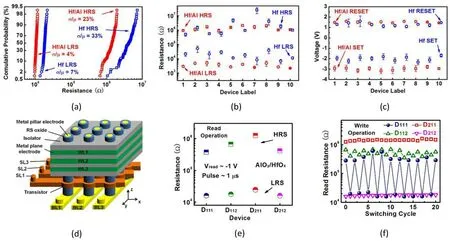
Fig. 10. (a) Comparison of the RHRS/RLRS distribution in 100 consecutive pulse cycles. (b) RHRS/RLRS extracted form 10 different devices. (c)Device-to-device comparison of the SET and RESET voltage distributions. (d)Schematic of the bit-cost 3D cross-point architecture using vertical RRAM array. The vertical MOSFET array as the BL selector addresses the individual cell in the array. (e)The read operation can be executed for the four RRAM devices in the 2×2 vertical array. (f)The set/reset disturb of devices in vertical array. Reprinted with permission from Ref.[101].
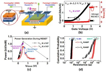
Fig. 11. (a) Schematic of HfO2 based 1T1R cell. (b) The I–V curves of reset operation for VG ramp scheme. (c) The power generation during the RESET process for the two program schemes. (d)Cycle-to-cycle resistance distribution in 1T1R cell for two programming modes.Reproduced with permission from Ref.[114].
4.2. Endurance
Endurance, also called cyclability, refers to the ability of a memory cell to sustain switching cycles under repetitive SET/RESET operation with a predefined resistance window.The endurance requirement is different according to the intended application. As high as 1015cycles in a non-stop condition is required for replacing DRAM-like storage class memory(SCM)applications,while 103cycles would be enough for Flash memory application. In the 3D architecture,insufficient endurance could significantly decrease the write/read margin.
A three-layer 3D vertical AlOx/Ta2O5?x/TaOyRRAM with extreme high endurance was demonstrated in Ref.[116].The schematic view and cross-sectional TEM image of the architecture are shown in Figs. 12(a) and 12(b). The resistive switching layer is located at the sidewall between TE and BE vertically. The vertical devices show high layer-to-layer uniformity and similar electrical characteristics as the planar counterpart. The pulse conditions utilized during set and reset processes are ?1.9 V,100 ns and 2.3 V,100 ns, respectively.As shown in Fig.12(c),the devices in every layer exhibit 1010switching endurance cycles. The degradation trend in vertical 3D devices, i.e., decreased HRS and stable LRS, are uniformity and show similar electrical characteristics as the planar counterpart. The retention results exhibit that both HRS and LRS could be kept more than 104s at 125°C without any degradation in the 3D architecture(Fig.12(d)).
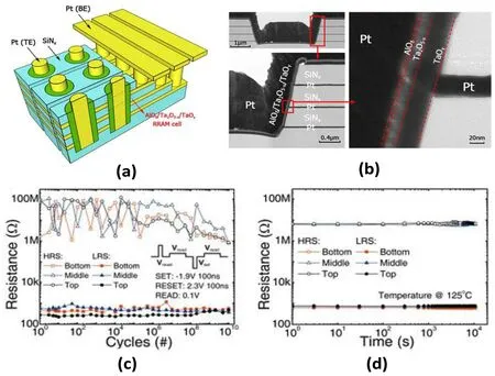
Fig.12. (a)The schematic view of 3D vertical RRAM.(b)The cross-sectional TEM image of 3D vertical RRAM cells with the structure of Pt/Ta2O5?x/TaOy/Pt. (c)All the devices demonstrate 1010 switching cycles. (d)The devices in triple layers show good retention. Reproduced with permission from Ref.[116].
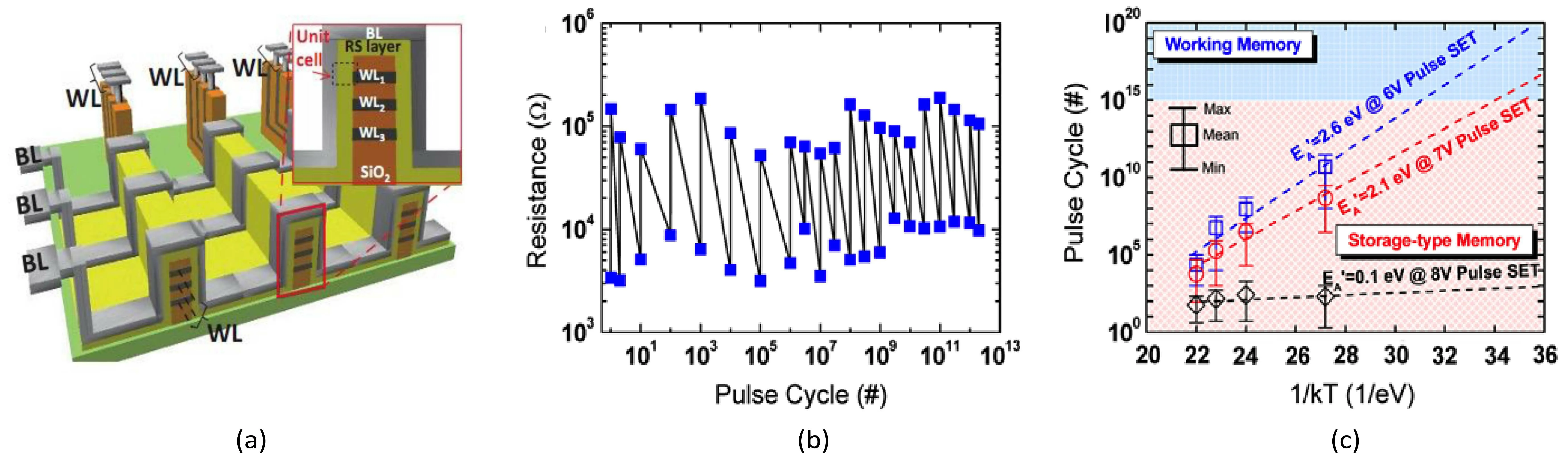
Fig.13. (a)Illustration of 3D V-RRAM arrays. (b)Typical pulse endurance of over 1012 cycles achieved at room temperature. (c)Arrhenius plot of the endurance cycle as a function of the magnitude of SET pulses of 100 ns.A fixed RESET pulse of 100 ns at 6 V was used.Reproduced with permission from Ref.[117].
Hsu et al.[117]demonstrated an extrapolated endurance of over 1015cycles at 100°C for a Ta/TaOx/TiO2/Ti vertical RRAM with a sub-μA operating current, with schematic shown in Fig. 14(a) and room temperature endurance shown in Fig. 13(b). It is the best endurance that has been reported and can satisfy the requirements for replacing DRAM as working memory(>1015cycles). They attributed the excellent endurance characteristics to the suppression of undesired overshoot current owing to the self-compliance and extremely low set current. The endurance would degrade to tens of cycles by increasing the set pulse to 8 V.The Arrhenius plot(Fig.13(c))of the endurance cycle elucidated that the irreversible hard breakdown was induced by the generation of new O2and VOdefects near the TaOx/TiO2interface under electrical stress.This paper provided a good enlightenment to improve the endurance.
According to the current reports, the endurance characteristic is strongly affected by pulse voltage/duration, compliance level, activation energy, dielectric thickness, filament temperature, and filament size/shape. Engineering the device architecture,doping in the switching layer,and adopting novel read/write schemes have been proved as the effective methods to optimize the endurance characteristic.
4.3. Retention
A data retention longer than ten years at thermal stress up to 85°C(operating temperature)and small electrical stress is expected for nonvolatile memory. The tail bits of the failure distribution become a limiting factor[118,119]for array level application. There are two types of retention failure: gradual degradation and abrupt degradation. For the retention failure with a gradual manner,[83,120–122]the resistance evolution can be extrapolated to find the failure point. However, a sudden resistance increase/decrease usually occurs rather than gradual transition during a typical retention process.[118,123,124]Then,an alternative method named temperature-accelerated method is adopted: varying the temperature/stress to record the timeto-failure/voltage-to-failure and draw the Arrhenius plot to extract the activation energy(Ea), and then extrapolate down to the operating temperature.
It is widely accepted that the retention loss is related to the diffusion of the VOor metal particle (M). The gradual resistance degradation is an accumulation process. For LRS, The VO/M concentration in filament is decreased by lateral diffusion from the surrounding region, resulting in degradation of the LRS retention characteristics. In the case of HRS,the vertical ions diffusion from the CF to the tunnel gap is a predominate parameter for the retention degradation. The abruptly retention failure phenomenon is correlated with a random process, which is often demonstrated by hopping-percolation model.[123]The cell resistance drastically increases when the most critical path is cut off during LRS retention measurement. HRS retention failure is due to reconstruction of the ruptured CFs due to the generation of VOby thermal activation process or an electric field effect.
In principle, the retention is dependent on various factors, such as filament size,[121,125]filament number,[126]active energy,[127,128]tunnel gap length,[120]and oxygen vacancy/metal ions concentration.[118,119,123,129]The enhancement of the LRS retention can be achieved by taking advantage of the stronger filament,by applying a larger compliance current,[121,125]or novel programming scheme,[118,119,123,130]or material engineering.[127,128]By a two-step forming method,[118]the filament size can be scaled down while keeping high density of the oxygen vacancy,and the retention can be improved even under low-current operation. Employing the metal oxide electrolyte with higher activation energy for metal ions diffusion as the electrolyte,the diffusion probability of the metal ions would reduce in contrast to the ionic conducting electrolyte. Thus, the retention of RRAM can be improved significantly.[131]Bilayer structure is always adopted to improve the reliability of the RRAM,[127,128]different thermodynamics abilities of metal caps(Ti,Ta,Hf,etc.) to scavenge oxygen from HfO2are expected to result in different oxygen vacancy profiles. The absolute value of oxygen vacancies will be increased by using the metal cap, thus improving the retention properties. Moreover, the retention characteristics can be significantly improved by tuning the filament morphology through adjusting the operating conditions.[131]Bai[116]reported both HRS and LRS of each layer could be kept more than 104s at 125°C without any degradation in three-layer 3D vertical AlOx/Ta2O5?x/TaOy(Fig.13(d)).
4.4. Distinguishable states
The distinguishable states of the memristor are also called the multi-level storage. Multi-level cell (MLC) capability characterizes the ability to store several bits in one cell. For general,the more the number of states,the better.It can greatly increase the storage density and computing power without increasing the cost. Currently, the maximum number of realizable states reported in the redox memristor can reach 64. According to the filamentary theory,the LRS resistance depends on the size of the conductive filament, while the HRS resistance lies on the gap length between filament and the electrode formed after the filament ruptured. There are two typical methods to realize the MLC operation through modulating the resistance states of RRAM.[8,90]During set process, the intermediate resistance states can be achieved by different set compliance. In 1T1R structure,MLC capability is highly depending on the controllability of the transistor. Xu et al.[135]revealed that the MLC margin would shrink due to the dynamic voltage drop on the transistor and memory cell. Controlling the RESET process is more favorable to achieve the uniform multilevel switching,which can be achieved both by changing the amplitudes or width of the RESET pulse.
For practical application,enough sense margins and tight uniformity of each resistance state are required for MLC operation.[116,133,134]The state fluctuation caused by stochastic nature of the conductive filament formation/rupture is a great challenge for the MLC capability.[83,113]The uniformity of the resistance states could be improved by optimizing the program and verify schemes.[133,135–138]Zhao et al.[133]proposed a pulse-training programming scheme to improve the uniformity of MLC without any read-verification operation.They adopted a train of pulses rather than a single pulse in RESET process to achieve better MLC control. By applying the novel scheme to a 3 bit/cell HfOx-based RRAM device,the uniformity of resistance distribution was improved up to 80%.Yu[137]investigated the read disturb and bipolar read scheme on multilevel RRAM-based deep learning inference engine,proposed a bipolar read scheme to enhance the resilience against the read disturb. A self-limited operation scheme for improving the uniformity of multi-level resistance states was proposed in Ref.[115], demonstrated in a Ta2O5/TaOxmemristive structure shown in Fig. 14(a). Compared to conventional operation scheme (left panel of Fig. 14(b)), the selflimited operation scheme could diminish the excessive current during SET and avoid the over-RESET during switching,thus achieving better multilevel storage(right panel of Fig.15(b)).The capability of MLC storage was also demonstrated in 3D vertically integrated RRAM cell.[84,116]
4.5. Scalability
Fig.14. Self-limited switching for uniformly regulating the values of both the low-and high-resistance states. (a)Self-limited operation scheme.(b)Improvement in the uniformity of multilevel switching due to self-limited switching. Left panel shows the multilevel switching uniformity of conventional operation scheme and right panel shows that of self-limited operation scheme. Reproduced with permission from Ref.[114].
Excellent scalability of RRAM cell has been demonstrated in several recent works. Joo et al.[139]theoretically studied the scaling limits of RRAM comprehensively based on atomic rearrangements calculation, by which the minimum number of atoms that need to be moved in order to create/rupture the conductive path with LRS current >1 μA and ON/OFF ratio >10 was estimated. A scaling limit of lateral size of 4 nm was suggested to grantee acceptable device performance and stability. By using Pt-coated silicon AFM tip as an electrode after directly contacting it with NiO surface,Lee et al.[14]successfully demonstrated an RRAM with ultrasmall cell size (10 nm×10 nm), which was approximately defined by the size of AFM tip. Tsai et al.[141]fabricated a sub-5 nm AlOxbased RRAM cell located at the intersection of the single-walled carbon nanotube(CNT)crossbar electrodes,the schematic and SEM are shown in Figs. 15(a) and 15(b).Stable resistive switching characteristics with on/off ratio of 5×10⁵and subμA operation current were achieved.The CNT resistance has a proportional relation with the LRS of RRAM cell, while they become independent as the CNT resistance gets below 10 M?(Fig.15(c)). Both set and reset voltages of the RRAMs were inversely proportional to the CNT resistance(Fig.15(d)). Impressive attempts to reduce cell size by using self-assembled oxide nanowire were made.[141–145]The fundamental scaling limits of RRAM device are greatly extended with the demonstration of the device with ultimate scaled size(1 nm–2 nm). The above-mentioned works present a promising potential of the scalable capability of RRAM device,however, an ultimate scaled device with fully integration into the CMOS process was still absent until the attempt from Govorean et al.[144]The world’s smallest HfO2-based RRAM cell with an area of less than 10 nm×10 nm was presented. This device was fabricated by 65 nm CMOS process.[145]Fast ns range switching time at low voltage and ultralow switching energy <0.1 pJ per bit were successfully demonstrated,as well as excellent endurance of more than 5×10⁷and large on/off ratio(>50).
The prediction of the scaling limit of 3D RRAM array is much more complicated than that of a single device. As shown in Fig. 16(a), as the thickness of WL/insulator stack in 3D VRRAM scales continuously, the sneak leakage path will inevitably occur in the selective layer between adjacent WLs. Xu et al.[51]proposed an elegant building block of 3D VRRAM using self-aligned self-selective RRAM to solve this problem (Fig. 16(b). Figure 16(c) shows the device structure design of TiN/TiOx/HfO2/Ru SSC device. Obvious hysteresis loop could be observed in the typical I–V characteristics of this SSC device(Fig.19(d)). Ultra-low off-state leakage current(pA)and operating current belowμA were achieved. The high nonlinearity in LRS guarantees the enough capability to suppress the sneaking current in high density array. The SSC also exhibits excellent endurance and favorable thermal stability(Figs.16(e)–16(f)). By successfully eliminating the interlayer leakage,the scaling limit of VRRAM could be extended beyond 5 nm which was later confirmed by experiments.[96]
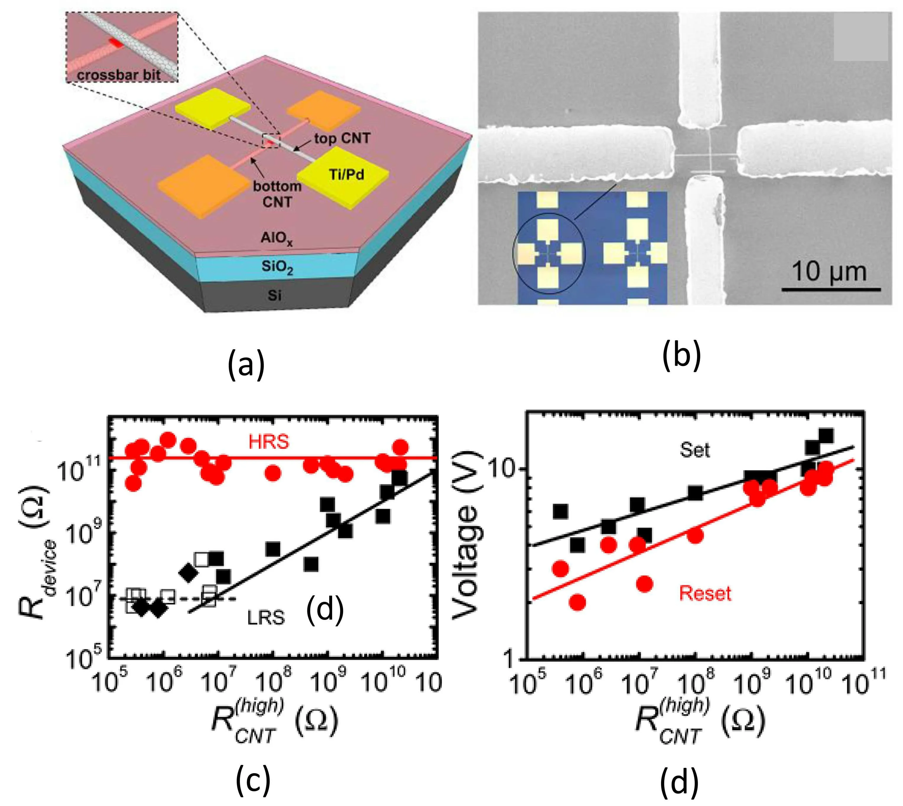
Fig. 15. (a) The AlOx RRAM cell sized sub-5 nm at the intersection of carbon nanotube crossbar electrodes. (b) SEM of the RRAM bit structure,including metal contacts to CNTs. (c) The LRS of crossbar RRAM is independent of CNT electrode resistance near 10 M?. The HRS of crossbar RRAM is independent of the CNT electrode resistance. (d) the operation voltages of the crossbar RRAM is dependent on the more resistive CNT electrode resistance. Reproduced with permission from Ref.[141].
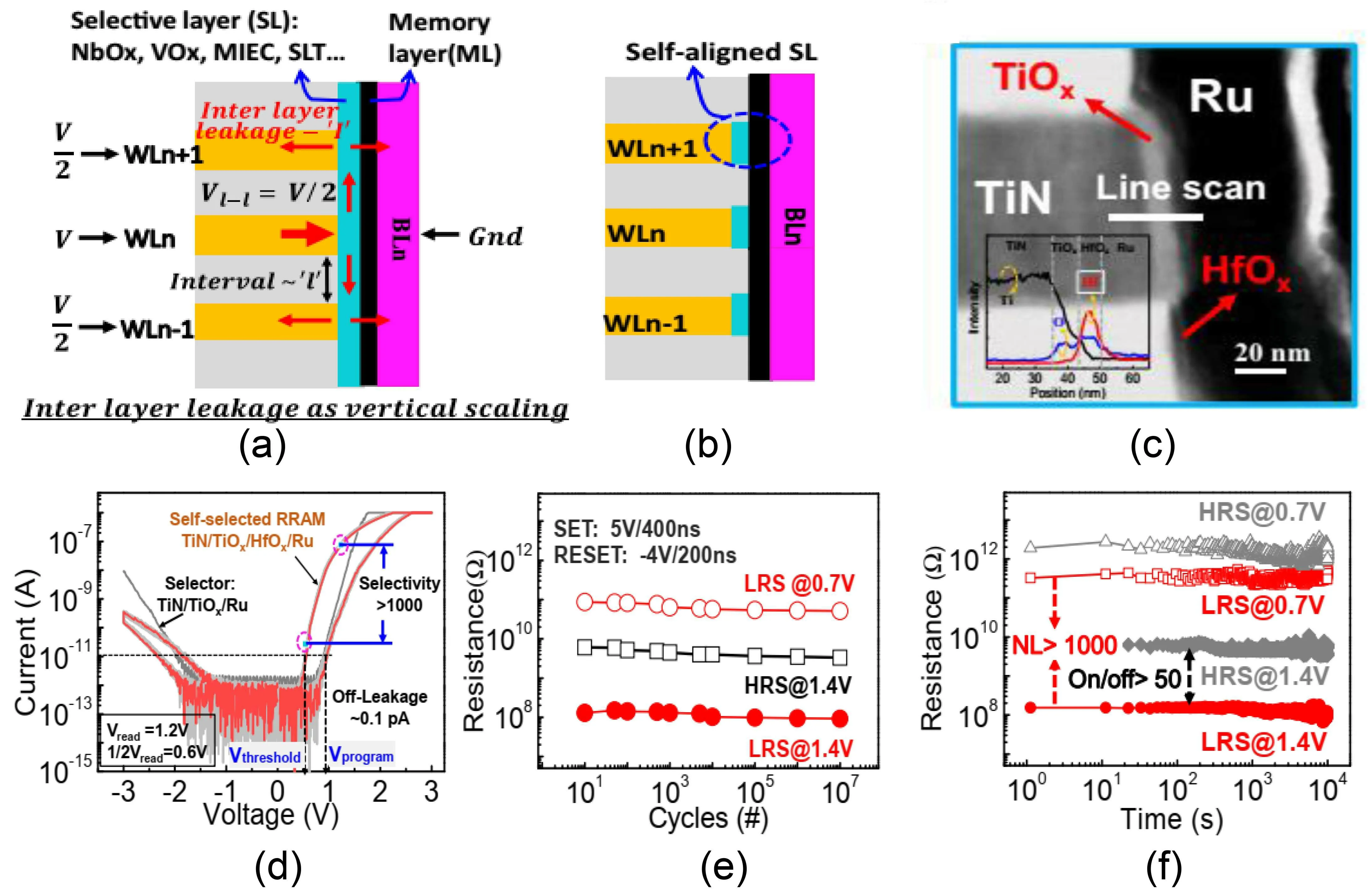
Fig.16.(a)The inter-layer leakage problem in VRRAM occurs with the thickness scaling.(b)Schematic of the proposed self-aligned VRRAM.(c)TEM image of cross section of TiN/TiOx/HfO2/Ru SSC device. (d)Typical I–V curve of the SSC.(e)The proposed SSC for VRRAM can switch >107 pulse cycles. (f)Both HRS and LRS of the SSC show favorable thermal stability. Reproduced with permission from Ref.[51].
5. Applications of 3D RRAM beyond storage
Resistive switching memory has potential application in the field of embedded circuit and high-density storage due to its excellent electrical properties, including high program speed,low consumption,and high density. More interestingly,the RRAM cells which show memristive switching behavior could be employed as synaptic devices for the neuromorphic and stochastic computing, which pave a new way to develop new computing system beyond Von Neumann architecture.The following section will focus on the topic of potential application of RRAM beyond storage.
5.1. Neuromorphic computing
Neuromorphic computation system which can imitate human’s brain, is superior to the conventional computer in recognizing various objects and processing imprecise sensory inputs through the energy-efficient and fault-tolerant computation. The human brain consists of 1011neurons and 1015synapses,[146]the former executes computation by collecting information from the other neurons and generating a spike, while the latter facilitates the computation by adjusting the strength as a respond to neuronal activity,as shown in Fig. 17(a). The mimicry of biological neurons and synapses by electronic devices is the crucial challenge for the hardware implementation of such massively parallel,three-dimensional,compact systems. The first FET-based synapse was proposed by Carver Mead,[147]but this synapse includes a large number of transistors and consumes significant energy and hinders the scaling trend of the neuromorphic chips.
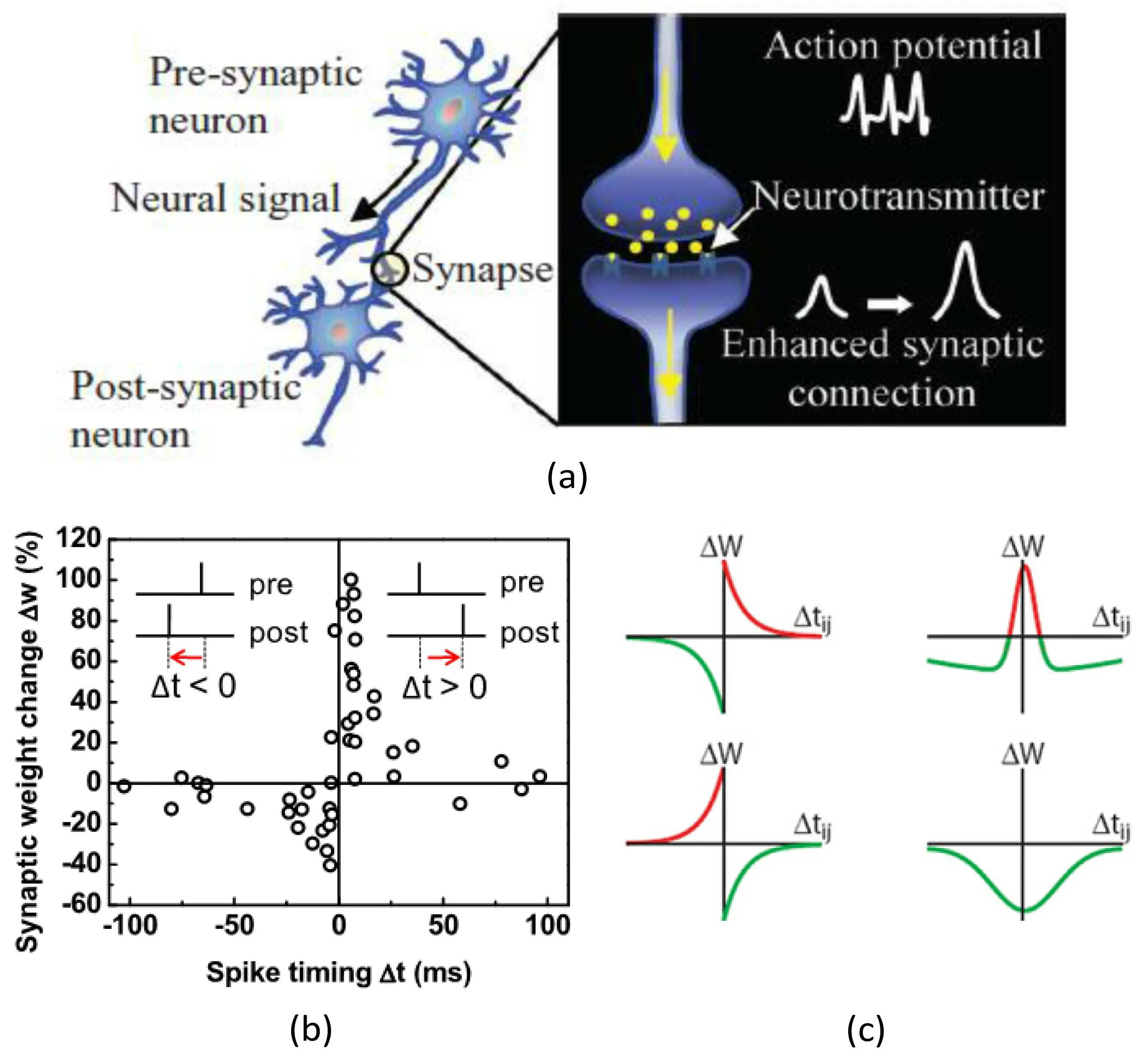
Fig.17. (a)The weight change in synapse is determined by the relative timings of neuronal spikes from the pre-synaptic neuron and the post-synaptic neuron.(b)In STDP measurements in hippocampal glutamatergic synapses,the synaptic weight change is a function of relative timing of pre-and postspikes. (c)Ideal STDP learning rules. Left: Asymmetric Hebbian learning rule and asymmetric anti-Hebbian learning rule. Right: Symmetric Hebbian learning rule and symmetric anti-Hebbian learning rule. Reproduced with permission from Ref.[164].
To achieve true human-level artificial intelligence, an electronic synapse with ultra-low power consumption, sub-10 nm scalability must be developed. To date, a broad spectrum of two-terminal non-volatile memory technologies with programmable conductance has been investigated to emulate synapses,such as phase change memory(PCM),[148–150]oxide based resistive switching memory(RRAM),[150–152]ferroelectric switches,[154,155]and carbon nanotube devices.[156–158]Among these candidates, RRAMs are more favorable due to their excellent scalability, fast switching speed, compatibility with CMOS technology and low energy consumption. The research activities in mimicking biological synapse by RRAM are growing rapidly since 2008.[151–153,159–163]
Activity-dependent synaptic plasticity is fundamental for learning and memory in neuronal systems,showing an analoglike behavior with numerous synaptic weight states modified by the neural activities in pre-synaptic and post-synaptic spikes.[164]The polarity or the degree of the synaptic weight change is influenced by the correlated activity of the presynaptic spike and postsynaptic firing, including the temporal relation, the spike rate, and the voltage amplitude.[151,153,164–167]Long-term potentiation(LTP)and long-term depression(LTD)are two opposite activity-dependent plasticity modifications,which are regarded as the bidirectional learning rule. According to the Hebb’s theory, synaptic weight change is a function of the relative timing of pre- and post-synaptic spikes.This behavior calls spike-timing dependent plasticity(STDP)which is a critical function for learning and memory in our brains.[166]The case a pre-synaptic spike precedes a postsynaptic spike repeatedly contributes to the potentiation of the synapse,whereas,if a post-synaptic spike precedes a presynaptic spike repeatedly,the synapse depresses. Figure 17(b)demonstrates the asymmetric STDP adapting the original data from Bi and Poo’s paper.[168]Figure 17(c)exhibits four typical forms of STDP which vary due to different spikes or different types of synapses, excitatory or inhibitory. Besides spike timing, the synaptic plasticity is greatly affected by the firing rate,spiking orders,and dendritic location. The spike-rate dependent plasticity (SRDP) is another central rule of learning,which reflects the influence of the synaptic activation frequency on the long-lasting modification.The synaptic efficacy is strengthened if the postsynaptic activity stays below a critical rate,and is conversely weakened under the high-frequency post-synaptic excitation. In addition,the LTP and LTD could be induced by repetitive coincident pre-and postsynaptic stimulations with low and high voltage amplitudes.
In the implementation of the synapse behavior,the terminals of the device are regarded as the pre- and post-synaptic sites, and the conductance/resistance of the device represents the synaptic weight or synaptic efficacy that refers to as the connection strength of the neurons. The more resistance states, the better the capacity and robustness of the neuromorphic systems will be. To implement synaptic function, the RRAM device must show the continuous tuning of conductance/resistance by voltage pulse. Yu et al.[23]firstly reported metal oxide-based RRAM with a gradual resistance modulation by hundreds of identical pulses. This synaptic device consumes sub-pJ energy per spike which is ×1000 reduction compared with the present-day PCM synaptic devices. They utilized the RESET process for adoptive learning since the RESET process is gradual and the SET process is abrupt. Li et al.[153]proposed the Ag/AgInSbTe/Ag structure which exhibits the reproducible gradual resistance tuning.Figures 18(a)and 18(b)demonstrate that the device conductance could continuously increase and decrease due to the consecutive positive or negative voltage sweep,which are also implemented under the pulse stimulation mode. The device conductance is equivalent to the synaptic weight.The synaptic weight can be modified in respond to a potentiating or depressing stimulus. Based on the memristive characteristic, the device was utilized to mimic the activity-dependent synaptic plasticity. The STDP learning rule was reproduced in the memoritive device by applying the paired spikes shown in Fig.18(c).The synaptic weight changes are plotted in Fig. 18(d) as a function of the time difference between the presynaptic spikes and the postsynaptic spikes.
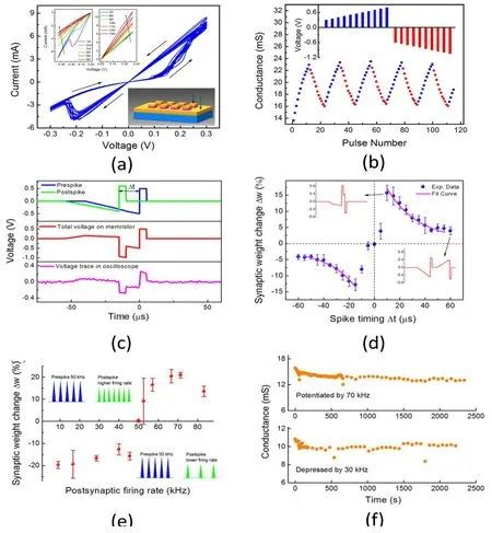
Fig.18. (a)The I–V characteristics of the Ag/AgInSbTe/Ag device. Up inset:the device conductance continuously increases(decreases)with the consecutive positive(negative)voltage sweep. Lower inset: the simple stacked structure of the memristor. (b) Repetitive gradual conductance modulation under pulse stimulation mode. Inset: the pulse scheme applied on the device to achieve stable and repeatable conductance tuning. (c)Pulse scheme used to implement STDP. The upper shows a negative temporal difference that exists between the pre-and post-spikes. The middle shows the effective voltage on the memristor. The lower shows the voltage trace captured by an oscilloscope. (d)The asymmetric Hebbian learning STDP rule of the memristor. (e) Implementation of SRDP in the memristor. (f) The changes in synaptic conductance following potentiation(upper)and depression(lower)stimulations.The synaptic efficacy is a long-term modification.Reproduced with permission from Ref.[159].
Based the asymmetric Hebbian learning STDP rule, the other three biological STDP forms according to Fig. 18(c)are also demonstrated in this device. STDP has been implemented in many other RRAM systems, including HfOx,[169]TiOx,[17,171]Ag2S,[159]AlOx,[161]TaOx,[172,173]IGZO,[174]Cu2S,[175]and PEDOT:PSS.[176,177]In addition to the STDP,SRDP is also implemented in the Ag/AgInSbTe/Ag memristor. Figure 18(e) shows the dependence of synaptic modification on the postsynaptic firing rate induced by 50 repetitive stimulations.[153]The synapse is depressed if the postsynaptic firing rate is below a critical rate(50 kHz),and potentiated when the rate is beyond the threshold. Meanwhile,LTD could be induced by post-synaptic frequencies,whereas LTP results from the high frequencies. Both the LTP and LTD depend on the stimulation frequency and the synaptic voltage. As shown in Fig.18(f),the synapse electric is potentiated and depressed by 70 kHz and 40 kHz,respectively. The nonvolatile property of the conductance further confirmed the long-term modification.
Extensive work has demonstrated that the brainlike associative learning, sequence learning, and pattern completion can be implemented with the synaptic devices.[151,160,162,164,176–180]Furthermore, computing applications with synaptic devices have focused on brain-inspired architectures and algorithms. Suri[162]proposed system-level simulations with binary CBRAM synapses by intrinsic probability programming methodologies. A 2-layer spiking neural network (SNN) is simulated for processing temporally video data. A video of cars passing on a freeway recorded with 128×128 pixel silicon retina is presented to the two-layered SNN consisting of about 2-million CBRAM synapses. The SNN shown here can be used as a prototype to realize more complex functions such as image classification, position detection, and target tracking. The same task of address-eventrepresentation (AER)video data of driving in a car is widely demonstrated by RRAM based neural network.
The RRAM array shows excellent potential for the neuromorphic application with comparable areal density and power efficiency with the human cerebral cortex. However,the practical implementation of such array is very challenging because of the inevitable device variability. The current reports about memristor neuromorphic network were all based on disconnecting each device from the crossbar for individual forming or using an individual switch transistor at each cross-point.[181–183]These approaches conflict with the goal of achieving a neuromorphic network with extreme high density. Merrikh[183]reported an experimental demonstration of a fully operational neural network based on an integrated,transistor-free crossbar with metal-oxide memristor. The uniformity and other important characteristics of the devices with Al2O3/TiO2?xbilayer were optimized firstly, providing a foundation for the implementation. The SEM image of the memristor crossbar is shown in Fig.19(a). A single-layer perceptron can successful be implemented by a 10×6 fragment of the memristive crossbar(Fig.19(b)). Figures 19(c)and 19(d)show the pattern classification experiment results. If the output signal is equal to the correct class of the applied pattern,the classification is successful. After 23 epochs, the perfect classification was achieved with the standard deviation of ten epochs. This work is regarded as the primary step towards much larger and more complex memristive neuromorphic networks.
Recently, Yao et al.[184]demonstrated a complete fivelayer convolutional neural network (CNN), one of the most important models for image recognition,implemented using a fully memristor-based hardware system. Based on the first integration system of multiple memristor crossbar arrays in the world, he successfully deployed a CNN on a highly consistent analog resistance array for the first time, and verified the prototype system of neural network processor based on memory integration. Figure 20(a)is the proposed memristor-based computing architecture for neural networks. The hardware system consists of 8 integrated PE arrays and other functional modules, which are implemented by the field-programmable gate array evaluation board (ZC706, Xilinx) and customized printed circuit board (PCB). Figure 20(b) presents the core PCB subsystem which consists of a memory integral unit based on the resistive memory array and the necessary functional modules implemented by peripheral discrete chips.Yao innovatively proposed parallel hardware strategies for hybrid training and replicating the same convolution kernel into different arrays. This hardware strategy can improve the convolution operation efficiency through parallel acceleration while accommodating the non-ideal fluctuation and noise of the device, and effectively solve the key problem of realizing the CNN. The experimental results show that the recognition rate can be equivalent to that of the software when calculating the complete convolutional neural network, as shown in Fig.20(c).
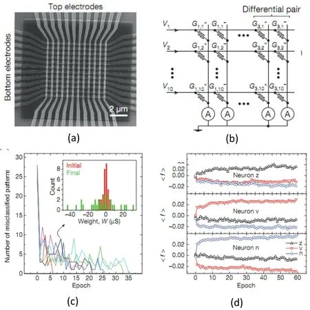
Fig. 19. (a) Integrated 12×12 crossbar with an Al2O3/TiO2?x memristor at each cross-point. (b) Pattern classification experiment in physicallevel description. The single-layer perceptron consists of 10×6 fragment of the memristive crossbar. (c)Pattern classification experiment results. After six training runs, different initial states were converged to the perfect value(zero). Insert: the distribution of weights in the initial state and after epoch 21. (d)The evolution of output signals,averaged over all patterns of a specific class. Reproduced with permission from Ref.[183].
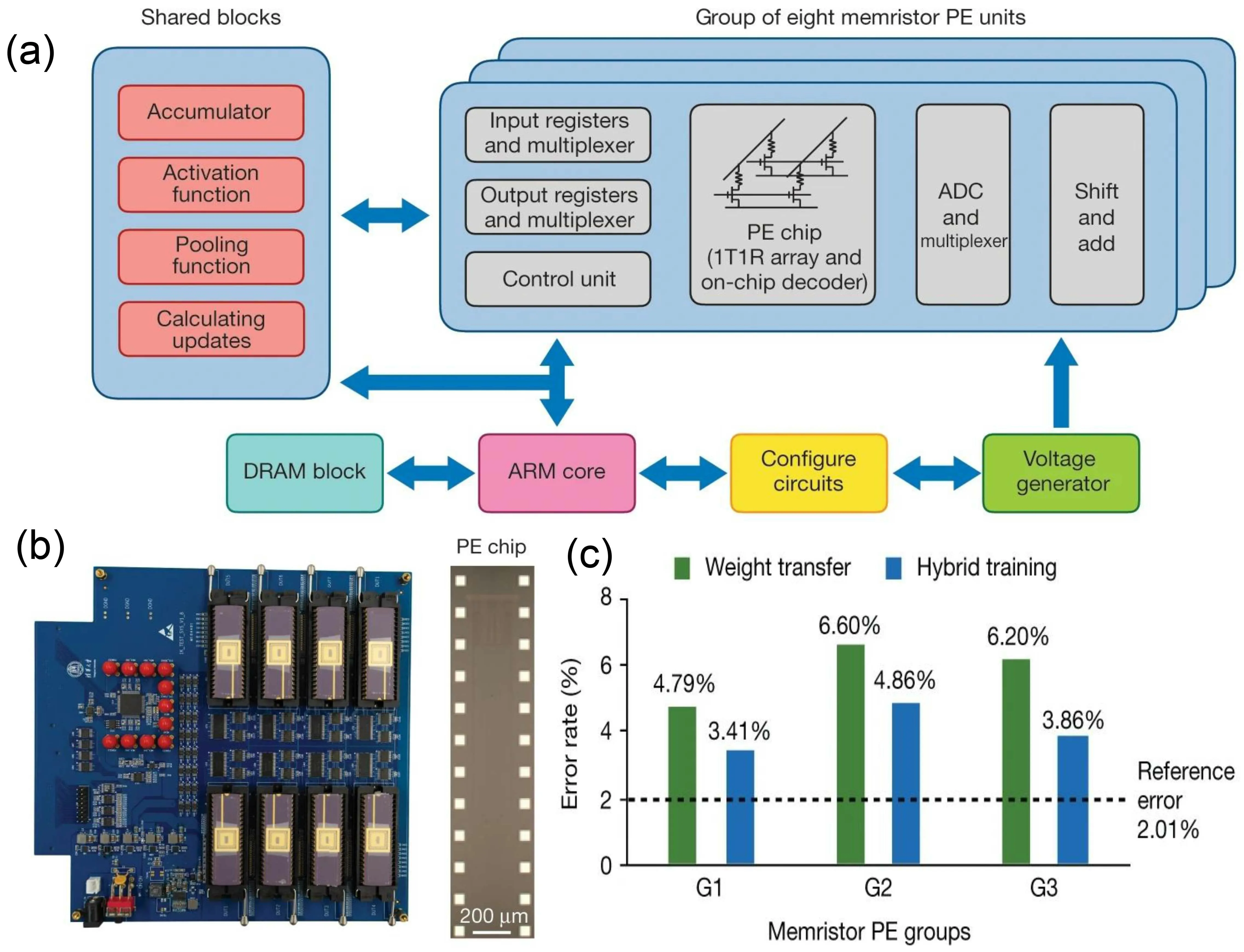
Fig.20. Fully hardware-implemented memristor convolutional neural network. (a)Memristor-based hardware system:schematic of the system architecture with eight integrated memristor PE units and other functional blocks. (b)The photograph of the integrated PCB subsystem and the image of a partial PE chip consisting of a 2048-memristor array and on-chip decoder circuits. (c)The error rate obtained on the test set after hybrid training. Reproduced with permission from Ref.[184].
With the unremitting efforts of the researchers, neural networks could be fully implemented in RRAM based systems and executed on site. The ingenious neural networks could transform the computing paradigms from high-demand,sequential digital operations into an activation-driven, parallel analogue-computing network. However, the current memristor-based systems are all constructed on regular 3D crossbar arrays. In human brains, the synaptic network consisting of billions of neurons is an intricate 3D architecture.As such, it is very attractive to extend the 2D cross-point array to 3D array to improve the integration density.[185–191]For the first time,Wang et al.[185]developed a 3D synaptic architecture based on Ta/TaOx/TiO2/Ti RRAM with cost-efficiency,as shown in Fig. 21. The 3D synaptic device shows selfrectifying characteristics to overcome the sneak current problem through inactive synapses in the network(Fig.21(b)).The STDP was successful implemented in the 3D synaptic device(Fig.21(c)). The result shows a similar trend as that of a biological synapse. The ultra-low power consumption as low as 7 fJ/spike in 3D architecture is comparable to that in biological synapses (Fig. 21(d)), suggesting promising potential of the breakthrough hardware for future neuromorphic computation. The linearity of synaptic weight updates is defined as the linear response of cell conductance to consecutive potentiation or depression inputs. The linearity of synaptic devices is a critical parameter for learning accuracy of RRAM based hardware neural network. The author[186]further proposed a new state-independent bipolar-pulse-training scheme to improve the linearity of weight updates, as shown in Fig. 21(e). The calculated accuracy under different operating modes is illustrated in Fig. 21(f). The ideal linear update scheme achieved nearly 100% training accuracy in 60 cycles. Compared with the unipolar-pulse-scheme,the bipolar-pulse-training-scheme with a lower NL improved the training accuracy significantly.
Further, the neuromorphic hardware design based on the 3D VRRAM is discussed by researchers. The 3D VRRAM with the plane WL structure has been investigated for deploying machine learning algorithms due to bit-cost scalability and simple structure.[188–191]For the neuromorphic applications of 3D V-RRAM, the pillar electrodes are utilized as the input vector and the plane electrodes as the weighted-sum outputs. Such operation scheme limits the number of output neurons that equals to the number of vertical layers. Li et al.[188]proposed a novel operation scheme to combine the selected lines and the word-plane electrodes as input vector,and all the BLs are designed as weighted-sum outputs. Figures 22(a)–22(c) demonstrate the operation scheme of 3D V-RRAM toward feedforward/backward inference(read)mode and weight update (write) mode. Compared to the 2D implementation,the proposed 3D V-RRAM implementation shows larger write margin for weighted sum/weight update, smaller latency, and energy consumption for weight update. This work demonstrates the attractiveness for building a monolithic 3D neuromorphic hardware platform. Li[189]improved the energy–delay product of neuromorphic computing by building the 3D vertical RRAM integrated with FinFET.Figure 22(d)exhibits the structure diagram. The 3D vertical RRAM is used for the system-level simulations as shown in Fig. 22(e). In the unsupervised winner-take-all visual system, the 3D architecture‘folds’neurons/synapses into balanced plane with dense connections. The interconnect RC effects and long sneak leakage paths are thus reduced. As shown in Fig. 22(f), the 3D architecture improves the energy–delay product by 55% and reduces VDDby 74%, which is a big improvement over the conventional 2D architecture.
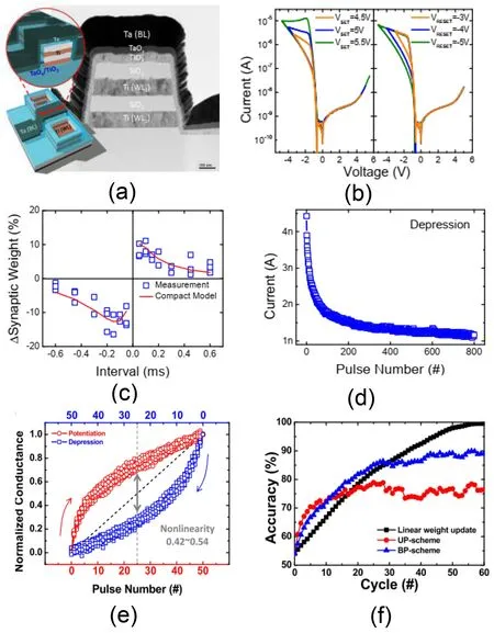
Fig. 21. (a) Cross-sectional TEM image of 3D Ta/TaOx/TiO2/Ti doublelayer V-RRAM as 3D synaptic network. (b) Multiple resistance states can be achieved by varying VSET or VRESET. (c)STDP measurement result in the 3D Ta/TaOx/TiO2/Ti device.(d)Depressing characteristics in the 3D device.The energy consumption per spike is as low as 7 fJ.(e)Normalized synaptic characteristics is optimized by the proposed the bipolar-pulse-training scheme. (f)Training accuracy with the training cycle under different training scheme. Reproduced with permission from Refs.[185,186].
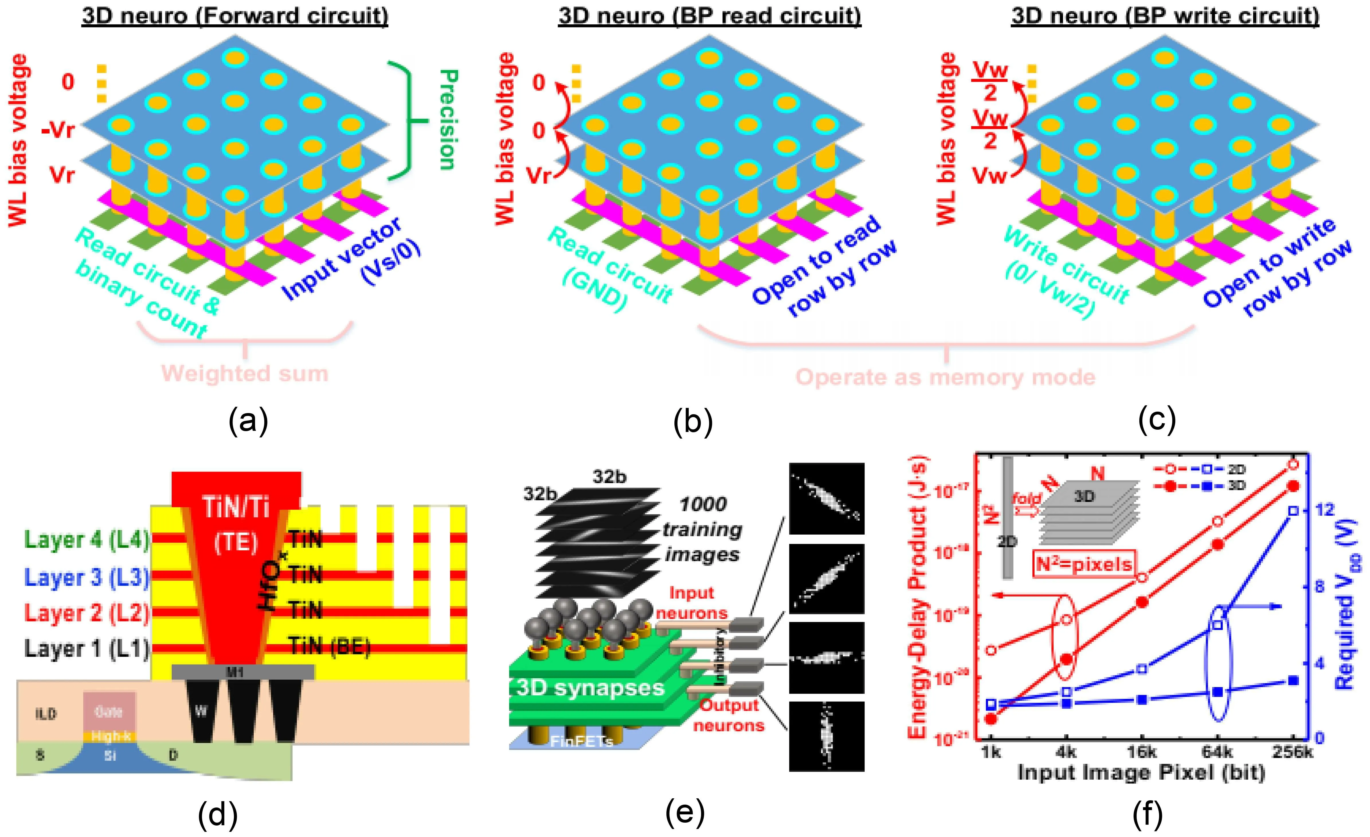
Fig. 22. Operation mode of 3D V-RRAM array for neuromorphic computing. (a) Feedforward/backward scheme for propagation mode to accelerate the weighted sum. (b)Read scheme and(c)write scheme for weight-update mode. (d)Schematic of 4-layer 3D RRAM integrated in FinFET platform. (e)A 3D neuromorphic visual system based on a 32×32×4 3D array. A winner-take-all network with stochastic learning rule is simulated for orientation detection.(f)SPICE-simulated energy–delay product and required VDD to program worst case-located synapses in 2D and 3D WTA networks. Reproduced with permission from Refs.[188,189].
Since the 3D VRRAM with even/odd WL structure can contain doubled cell bits compared to the WL plane structure,it exhibits outstanding area efficiency and high potential in neural network implementation. However, the increased interconnect lines due to the split WLs require a sophisticated control mechanism to access the cells and exacerbate the sneak path issue. To minimize the side effects induced by the increase of interconnects, Kim et al.[191]proposed the hardware design through a more balanced structure along the three orthogonal directions. In this design, the input data was fed through the vertical pillar electrodes and the output was detected at the WLs. By this approach, a more balanced array configuration on layers, i.e., similar row and column lengths, was achieved and the elongated sneak path was reduced efficiently. Furthermore, they defined a weight adjustment method to harmonize with the use of even/odd lines and devised a sequential operation to ensure to program only intended cells. The SSC with high nonlinearity was also utilized to alleviate the sneak path issue. This work verifies the effectiveness of the even/odd WL structure for neuromorphic system implementation.
As neural networks have been rapidly evolving, 3D vertical RRAM is considered as the most promising candidate to increase the density of neuromorphic circuits. Although both of 3D VRRAMs organized in the plane WL structure and the even/odd WL structure show potential applications. The complicated interconnection of 3D VRRAM makes the design more challenging, mainly due to several issues, such as the vulnerable unselected cells that share the same lines with the selected cells are more easily to be affected and the sneak leakage path per area increases. So, 3D VRRAM requires more carefully designed operations before building a monolithic 3D neuromorphic hardware platform.
5.2. 3D CMOL circuit
Hybrid CMOS/molecular circuits(CMOL)are a promising hybrid structure that extends the Moore’s law 10 to 15 years beyond the so-called “redbrick wall”.[192–194,194]Figure 23 demonstrates the basic idea of CMOL circuits, which corporate the CMOS subsystem with nanowire crossbars and simple two-terminal molecular devices (Figs. 23(a) and 23(b)).[195]The CMOS subsystem exhibits the advantages of flexibility and high fabrication yield. The typical I–V curve of the two-terminal molecular device is shown in Fig.23(c). For the hybrid circuits,the efficient implementation of the integration of CMOS and nano crossbars is the main issue. This challenge can be overcome by area-distributed interface between the two elements,using conic-shaped vertical plugs“pins”in 3D CMOL.Because of the self-assembly of the molecular devices on the nanowire crossbar,the fabrication of the CMOL is much cost effective without precise alignment. Furthermore,the density of active devices in CMOL circuits is estimated up to ~1012active devices per cm2since the minimum feature of the CMOL is defined by the size of a certain molecule rather than the traditional lithography.[194]Borghetti et al.[196]achieved a 100-gate-scale hybrid CMOS/memristor circuit,in which memristive TiO2?xfilm is integrated onto a foundrybuilt CMOS platform. An area- distributed CMOL-like interface with tilted crossbar was fabricated with nanoimprint technology.
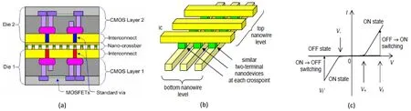
Fig. 23. (a) Hybrid circuit cartoon, (b) crossbar topology, and (c) micrograph of array of the memristive devices, and typical switching I–V curves. Reproduced with permission from Refs.[195,198].
The most fundamental application of the 3D CMOL circuit is the memory category, considering as the extension of the RRAM.[194,196,198,199]For such memory, each memristive device plays the role of a single-bit memory cell, while the CMOS subsystem works for the peripheral including input/output,coding/decoding,line driving,and sense amplification. The hybrid CMOS/memristor circuits could potentially combine all the advantages of the CMOS chip and the RRAM–high yields,cost efficient,high speed,low energy,and high endurance of the memory. Zhong and Chen[200,201]have taken the first experimental steps to implement the hybrid memories.
The high function density is one of the attractions of the CMOL memory,which can be approached by larger crossbar array. As the array size increases,the readout delays and voltage drop across crossbar wires become longer, as well as the leakage current via the memristor.When combined in circuits,the memory cells are organized in roughly square arrays with multiple cells sharing row(word)and column(bit)lines. The integration of a traditional transistor with the memory cell can enable unique access(read/write)to the row of cells at a time via bit lines by asserting the corresponding select word line(Fig.24(a)).However,the peripheral area overhead(i.e.,sense amplifiers,decoders,etc.) is proportional to N×logN for the N×N crossbar array, which causes large area waste.[193,194]The passive crossbar is a much denser alternation, in which the select functionality is implemented via the diode-like I–V of the cross-point device (Figs. 24(b) and 24(c)). Therefore,the strong nonlinearity in the I–V is the expectation for the RRAM in the context of passive crossbar memories.
Novel defect and fault tolerance schemes must be considered for the CMOL memory. Two major techniques, the memory matrix reconfiguration and error correction code techniques (ECC), are always applied for increasing the defecttolerance.[202,203]Memory matrix reconfiguration means replacing memory array lines containing bad cells by spare lines. Dmitri et al.[198]demonstrated that by using the best(but hardly practicable) reconfiguration and block size optimization, hybrid memories may achieve defect tolerance up to ~15%. It is said that CMOL memories may be the first technology to reach the terabit frontier.
The most important application of CMOL technology may be in reconfigurable Boolean logic circuits[24,199,204,205]whose structure resembles the cell-based field programmable gate arrays (FPGAs). Figure 25(a) shows the schematic of original CMOL FPGA. The basic cell consists of an inverter and two pass transistors that serve two pins as the cell input and output. The cells connect to the nanowire/molecular subsystem via two pins (Fig. 25(b)). Each pin of the cell can be connected through a nanowire–nanodevice–nanowire link within a square-shaped“connectivity domain”around the pin when turning programmable diode. The RRAM here provides resistance states as the Boolean logic stage,and allows circuit mapping on CMOL fabric and its reconfiguration around defective nanodevices. Any logic function can be implemented by the logic gates(e.g.,NOR,NAND)by CMOL-FPGA.
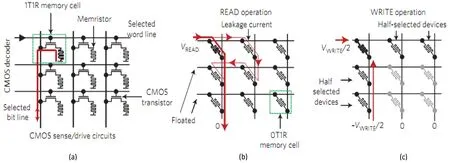
Fig.24. The integrated architecture. (a)The active array. A 1T1R cell architecture enables unique access(read/write)to the cells in a selected row at a time via bit lines by asserting the corresponding select word line. (b) The passive crossbar memory. The select functionality is implemented via the diode-like I–V of the cross-point device. (c) Strong nonlinearity in switching dynamics helps avoid another problem specific to 0T1R architecture. Reproduced with permission from Ref.[197].
The CMOL FPGA circuits could improve the density by two orders of magnitude over purely CMOS FPGA circuits since the configuration information can be stored by the memristor in CMOL FPGA circuits while the implication of the configuration information in traditional FPGAs typically consumes 50%–90% of the chip area.[199]This advantage is confirmed in Ref.[24],where the CMOL FPGA circuits showed significant advantage of area-efficiency with manageable power consumption and high defect tolerance(above 20%of bad nanodevices). Xia et al.[204]implemented the first CMOL FPGA circuit by integrating the TiOxmemristor crossbar on top of a CMOS substrate using nanoimprint lithography,as shown in Fig.25(c). The size of each cell in this 8×8 array is 50μm×50μm.The logic part provides three types of computing elements: logic gates,flip-flops,and repeaters. By configuring the memristors properly, logic functions including OR, AND, NAND, NOR, and a positive-edge triggered D flip-flop can be implemented in the hybrid circuits. The equivalent computing circuits and the correspondingly measured truth tables for the logic gates of the hybrid circuits are shown in Fig.25(d).
Fig.25. (a)The original CMOL,(b)a single CMOS cell. (c)A successful experimental demonstration of the CMOL FPGA:CMOS layer fabric on a die and possible wiring for digital circuits using memristors. (d)The equivalent computing circuits, visualized digital results, and the measured truth tables for the logic gates in the hybrid circuits. Reproduced with permission from Ref.[206].
The properly designed CMOL circuits show high defecttolerant, allowing ~10% of bad bits in memories,[203]~20% for FPGA-like logic,[199]and more than 40% for some neuromorphic circuits.[207]The most exciting application of CMOL circuits is emulating the neuromorphic networks(“CrossNets”).[9,204,208]In these circuits,the neural cell bodies(“somas”)are implemented in the CMOS subsystem,and axons and dendrites are emulated by crossbar nanowires. This application concept has been comprehensively addressed in the previous section.
6. Conclusion and perspectives
As an advanced extension of two-dimensional passive crossbar array, the three-dimensional architecture should not only overcome the common problems that the passive arrays face,such as sneaking current path,voltage drop on line resistance,scaling,etc,but also need to deal with more challenging technological issues, such as complexity of fabrication process, thermal crosstalk, variation, etc. In order to suppress the sneaking current paths, each cell at the cross-point node should have nonlinear characteristics,which could be realized by explicitly introducing separate selector device or implicitly making the memory device self-selective. A variety of selector devices have been developed in the past few years, such as MIT or threshold switching device, bidirectional Schottky diode, and nonlinear tunneling device. Although great progresses have been made on the selector device with respect to large nonlinearity and high current density, additional attention should be paid on the aspects of CMOS compatible materials developing,off-state leakage reduction,and voltage window increment.
Promising cross-bar array designs featured 1S1R and 1D1R were already demonstrated as prototypical 3D stacked horizontal ReRAM(H-RRAM)arrays. Therefore,the stacked planar crossbar array at the current stage becomes the major choice for test chip designing and more readily for fabrication with mature CMOS platform. The recent demonstrated high volume 3D RRAM test chips(Panasonic’s 8 Mb chip and Sandisk’s 32 Gb chip) are all based on stacked planar crossbar.However,the cost advantage of VRRAM architecture over stacked array is competitive,which urges the research community making continuous effect to develop satisfactory SSC cell.The strategy of designing an SSC device should eliminate the secondary effect of the memory switching on its selectivity as much as possible.It is more difficult for self-selected device to tune its nonlinearity and memory performance separately considering the motions of oxygen or metal ions during memory operation may inevitably influence the barrier properties contributing to the nonlinearity. In this sense,the hybrid structure with dedicated threshold switching layer and memory switching layer should be a good choice. More efforts need to be made in the direction of avoiding interface diffusion with no material contamination, reducing the switching current with less thermal effect,and enhancing the reliability after continuous reading and writing.
For practical application,the main target of 3D RRAM is for massive data storage,high endurance as 1015for DRAM is not necessary. This type of memory should not replace the flash because of the mature fabrication technology and improved performance for the traditional flash memory. It may be used as a complementary component in the memory hierarchy, similar to the X-point. The 3D RRAM would improve overall system performance by serving as a non-volatile cache/buffer memory between a storage and the processor.
Beyond mere data storage, the RRAM technology also offers other applications, such as neuromorphic computing.The high similarity between the RRAM device and biological synapse makes the RRAM devices possibly serve as electric synapses to build a brain inspired frontier neuro computing system. Since 2008, the research activities in this area have been growing dramatically. A variety of synaptic functions such as SDTP,SRTP,LTP,LDP,etc have been demonstrated.Although the 3D RRAM array shows excellent potential for the neuromorphic application with comparable areal density and power efficiency with the human brain, the practical implementation is very challenging because of the complicated interconnection of 3D VRRAM. The device variability and the sneak current should be well addressed. Most of the system level demonstrations were only performed by simulation.Much research efforts are still needed to explore the resistive switching device with better uniformity and lower power consumption. The 3D VRRAM requires more carefully design before building a 3D neuromorphic hardware platform.
猜你喜歡
金秋(2023年6期)2023-07-22 09:19:52
作文周刊·小學(xué)二年級(jí)版(2022年24期)2022-06-18 14:30:28
江蘇科技報(bào)·E教中國(guó)(2022年5期)2022-05-11 22:54:28
快樂語(yǔ)文(2021年18期)2021-12-22 09:00:38
水動(dòng)力學(xué)研究與進(jìn)展 B輯(2018年6期)2019-01-05 08:09:02
智富時(shí)代(2018年6期)2018-08-06 19:35:08
Acta Mathematica Scientia(English Series)(2018年3期)2018-07-23 08:41:10
寶藏(2018年1期)2018-04-18 07:39:34
中國(guó)三峽(2017年3期)2017-06-09 08:14:59
校園英語(yǔ)·上旬(2015年4期)2015-05-30 14:30:09

- Chinese Physics B的其它文章
- Process modeling gas atomization of close-coupled ring-hole nozzle for 316L stainless steel powder production*
- A 532 nm molecular iodine optical frequency standard based on modulation transfer spectroscopy*
- High-throughput identification of one-dimensional atomic wires and first principles calculations of their electronic states*
- Effect of tellurium(Te4+)irradiation on microstructure and associated irradiation-induced hardening*
- Effect of helium concentration on irradiation damage of Fe-ion irradiated SIMP steel at 300 °C and 450 °C*
- Optical spectroscopy study of damage evolution in 6H-SiC by H+2 implantation*