
Influences of supply voltage on single event upsets and multiple-cell upsets in nanometer SRAM across a wide linear energy transfer range?
2021-05-06 08:56:00YinYongLuo羅尹虹WeiChen陳偉FengQiZhang張鳳祁andTanWang王坦
Chinese Physics B 2021年4期
關(guān)鍵詞:陳偉
Yin-Yong Luo(羅尹虹), Wei Chen(陳偉), Feng-Qi Zhang(張鳳祁), and Tan Wang(王坦)
State Key Laboratory of Intense Pulsed Radiation Simulation and Effect,Northwest Institute of Nuclear Technology,Xi’an 710024,China
Keywords: supply voltage,single event upsets,multiple-cell upsets,65-nm SRAM,double DICE SRAM
1. Introduction
With the feature size of the device scaling down, the supply voltage and single event effect (SEE) critical charge spontaneously decrease, thus leading the SEE sensitivity to increase.[1,2]Static random access memories (SRAMs) are widely used in the ultra-large scale integrated circuits and electronic systems of spacecrafts. But the SRAMs are very sensitive to SEE, so the studies of SEE in SRAMs always receive much attention. Low power consumption is often expected for devices operated in space environment. Lowering the supply voltage is usually an effective approach to reducing the power consumption.[3,4]However, it is generally considered that the reduction of supply voltage will cause the single event upset (SEU) critical charge quantity in SRAM to decrease,which will exacerbate the occurrence of SEUs and multiplecell upsets (MCUs).[5,6]Even if the bit-interleaving technology is used in the layout design, the probability of cumulating multiple-bit upsets (MBUs) in a logical word will still increase obviously, resulting in the failure of error detection and correction(EDAC)technology. Therefore,a higher scrubbing frequency needs adopting in order to prevent the MBU from occurring, which in turn causes the power consumption to increase.[7]Eventually,lowering the supply voltage may not have to bring the reduction of total power consumption. So it is necessary to study whether the reduction of supply voltage will certainly lead the SEU and MCU to significantly increase under the actual application environment,which will help determine the optimal voltage value to make a comprehensive balance between the effective control of space SEU rate and the reduction of power consumption.
Some researches have been carried out about the dependence of SEU and MCU on the supply voltage in nanometer devices.[8–15]When the voltage ranges from 0.75 V to 1.2 V, the scaling voltage will cause the SEU cross section to increase in 90-nm, 65-nm, 45-nm SRAM, and 20-nm DFF for low energy protons, low energy muons, alpha particles, and heavy ions with low linear energy transfer(LET).[8–11]For 14-nm/16-nm FinFET D flip-flop(DFF),SEU cross section increases with the decrease of voltage at 0.5 V–0.8 V when heavy ion LET ranges from 0.89 MeV·cm2/mg to 58.78 MeV·cm2/mg.[12]When the device operates at ultra-low voltage,the device can only retain data,but read operation or write operation cannot be performed normally. In this case,even low energy electrons can also induce the SEU through direct ionization in 45-nm and 28-nm SRAM at 0.45 V and 0.55 V, the SEU cross section increases with the decrease of voltage.[13]Spallation neutron source and alpha particles will cause the SEU cross section to increase in 65-nm SRAM across a wide range of supply voltage from 1.0 V to 0.3 V.But the ratio of MCU increases with the voltage increasing above 0.5 V for spallation neutron source or with the voltage decreasing less than 0.5 V for alpha particles.[14,15]
Previous researches about the effect of scaling voltage on SEU in nanometer SRAM mostly focused on neutrons, alpha particles, and electrons. Only a few papers about heavy ion experimental study based on DFF were published. In an actual space environment, the LET values of heavy ions range from 0.002 MeV·cm2/mg to 120 MeV·cm2/mg. The influence of the supply voltage on the SEU and the MCU across a wide LET range are rarely reported in nanometer SRAMs with different layout designs. In this work, the effect of lowering the voltage on the SEU and the MCU are investigated in non-hardened and radiation-hardened 65-nm SRAMs with LET ranging from 0.35 MeV·cm2/mg to 84.6 MeV·cm2/mg.Because the SRAM operating in ultra-low voltage region cannot be read nor written during irradiation,the logical addresses and the stored data of memory cells with the occurrence of SEU are recorded only after the SRAM is irradiated to a specified fluence and the supply voltage is returned to the nominal voltage. It is effective to study the effect of voltage on SEU,but the probability of false MCUs which are caused by different ions striking on adjacent cells obviously increases due to the accumulation of a large quantity of SEUs.[16,17]Therefore, it is difficult to distinguish the quantities and topological patterns of MCUs with different orders accurately. In this study, the supply voltage in 65-nm SRAM is changed in a range of±10%of the nominal voltage. During the irradiation,the stored data of cells are read back continuously once per second and compared with those from the previous read cycle. The operating frequency of the testing system is 8 MHz,which takes 4 ms to finish one test of the whole addresses in the SRAM.Therefore,the number and topological patterns of MCUs with different orders can be effectively acquired. The influence of voltage variation on SEU, MCU and single cell upset(SCU)are further studied.
The rest of this work is organized as follows. In Section 2 described are the device characteristics of two types of SRAMs, irradiation test facility and the method of data processing. Experimental results are presented in Section 3. In Section 4,the key topic is discussed in detail. The conclusions are drawn from the present study in Section 5.
2. Experimental details
2.1. Device under test
Both SRAMs are fabricated by a bulk CMOS 65-nm technology.The“6T”denotes a 32-k×8-bit SRAM with standard 6-transistor(6T)cells. The area of the cell is 0.62μm2. The“DICE” represents a 16-k × 8-bit SRAM with interleaving double dual interlocked cells. The area of single DICE cell including 12 transistors is about 5.2 μm2. Through sharing the area between two cells, the area of double DICE cells is only about 6μm2, thus increasing effectively the spacing between sensitive nodes within a DICE cell. For both SRAMs,the nominal supply voltage is 1.2 V for memory array and 3.3 V for peripheral I/O circuit. The thickness of back end of line(BEOL)is about 5.7μm with six copper-interconnection layers.
The SRAMs are tested with logical checkerboard pattern“55H”in a dynamic mode.The memory content of the SRAM is read back continuously during the irradiation. The logical address and data of memory cells with SEU are recorded at the end of each read cycle. The SEU testing is performed at three different supply voltages ranging from nominal ?10%to+10%,i.e.,at 1.08 V,1.2 V,1.32 V.
2.2. Heavy ion irradiation facility
Heavy ion SEE testing is carried out on the HI-13 Tandem Accelerator in China Institute of Atomic Energy and Heavy Ion Research Facility in Lanzhou (HIRFL). Table 1 summarizes the ions used in the testing. The LET values at the surfaces of devices are given. Due to the limitation of beam time and beam schedule, the influence of supply voltage on SEU and MCU are investigated in the 6T SRAM with only using C,Cl,Ti,Br ions,and in the DICE SRAM with only Br,Ta ions.Irradiations are carried out with the normal incidence of ions.

Table 1. Ions used in heavy ion SEE testing.
2.3. Low energy proton testing
In order to supplement the SEU data with LET less than 0.5 MeV·cm2/mg, the low energy proton SEU testing is performed at the EN Tandem accelerator in the Institute of Heavy Ion Physics at Peking University. The proton energy of the accelerator can be tuned from 1 MeV to 10 MeV. The protons with the initial energy 1.2 MeV are reduced by using Al foils with different thickness values,thus producing the lower energy protons (down to 0.20 MeV). After the proton energy corresponding to SEU peak cross section is acquired, the dependence of SEU cross section on supply voltage is further investigated at the corresponding energy.
2.4. Data processing
After the logical address and data of memory cells with SEU are recorded, the number and topological pattern of MCUs with different orders are analyzed and studied statistically based on the relation between the logical bitmap and the physical bitmap. Further, MCU ratio, MCU mean, and SEU,SCU,MCU event cross section are counted.
Two kinds of SEE cross sections are presented here.[18,19]One is SEU event cross section σE?SEU, which is the sum of SCU and MCU event cross sections. The SEU event Eventi?cellis counted only once and is not weighted.

where i is the number of affected cells in one SEU event,Eventi?cellis the number of SEU events with i–cell upsets.
The other is the conventional SEU cross section σU?SEUwhich is written as

The MCU mean represents the average number of SEUs caused by an SEU event.
MCU ratio can be expressed as

3. Experimental results
3.1. Influence of voltage on SEU and MCU in 6T SRAM
Figure 1 shows SEU, SEU event, and MCU event cross sections as a function of LET in 6T SRAM at nominal voltage of 1.2 V. During the low energy proton SEU testing, the average proton energy corresponding to proton SEU peak cross section is 0.77 MeV.Based on SRIM-2013,the proton energy distribution within the sensitive region is simulated after 0.77-MeV protons have passed through the BEOL layer of the device under test(DUT) described in Subsection 2.1. The simulation result shows that the average proton energy within the sensitive region is about 270 eV,thus the average LET value is 0.35 MeV·cm2/mg.Because low-energy protons cause SEU through direct ionization,the peak SEU cross section and the corresponding LET are also drawn in Fig.1.
As shown in Fig.1, the SEU cross section and SEU event cross section are both the same, specifically,1.73 MeV·cm2/mg and less,which indicates that all the SEUs come from SCU.When the LET is 4.2 MeV·cm2/mg,there is a slight difference between these two kinds of cross sections.A small number of MCUs appear, and MCU event cross section is low. With the LET increasing further, the SEU cross section and SEU event cross section show a significant difference. The MCUs become more serious,the MCU event cross section even approaches to the SEU event cross section at a high LET.
Figure 1 also shows that the fitting results of these three kinds of cross sections with the Weibull function. The LET threshold of SEU and MCU are about 0.28 MeV·cm2/mg and 2.8 MeV·cm2/mg,respectively. The SEU saturation cross section is 1.85×10?8cm2, and the SEU event saturation cross section is 6×10?9cm2. The former is over three times as great as the latter, which indicates that an incident ion with high LET can cause an average of three cells to upset simultaneously.

Fig.1. SEU cross section, SEU event cross section, and MCU event cross section versus LET in 6T SRAM.
Figure 2 shows the influences of supply voltage on SEU cross section with different LETs in 6T SRAM.When the LET is 0.35 MeV·cm2/mg,the SEU cross section increases 13 times from 2.67×10?12cm2at 1.32 V to 3.5×10?11cm2at 1.08 V with the reduction of supply voltage. With LET increasing to 1.73 MeV·cm2/mg, SEU cross section only increases 1.3 times from 8.01×10?10cm2at 1.32 V to 1.04×10?9cm2at 1.08 V. The SEU cross section exhibits a weak increase. As LET increases to 13.1 MeV·cm2/mg and more,the SEU cross sections almost keep unchanged with the decrease of voltage.These results indicate that the SEU sensitivity to the voltage variation decreases with the increase of LET in non-hardened 6T SRAM.

Fig.2. SEU cross section versus supply voltage with different LETs.
For LETs with 13.1,21.8,and 42 MeV·cm2/mg,the SEU cross section is larger than the SEU event cross section, and the SEU event consists of SCU event and MCU event.Aiming at these three LETs,the influence of scaling down the voltage on MCU mean, MCU ratio, and SEU, SCU, different-order MCU event cross sections, are listed particularly in Table 2.In this table, MCU ratio, MCU mean, and MCU event cross section obviously rise with the increase of LET.However,the influence of lowering the voltage on MCU mean and MCU ratio do not follow the consistent trend for different LET values:MCU ratio and MCU mean increase with the reduction of voltage only for the LET with 13.1 MeV·cm2/mg.The MCU event cross sections increase for LETs with 13.1,21.8 MeV·cm2/mg with the voltage lowering. Interestingly, the sum of MCU2–MCU4 event cross sections increases,but the sum of MCU5–MCU8 event cross sections decreases. For 42 MeV·cm2/mg at which MCU event cross section is located within the saturation region, the MCU event cross section, the sum of MCU2–MCU4 event cross sections and the sum of MCU5–MCU8 event cross sections have no obvious changes at different voltages. On the other hand, the highest-order MCU event cross section decreases to a certain degree with the voltage lowering for three LET values. For example,the highestorder MCU6 event cross section with 13.1 MeV·cm2/mg decreases by 3.3 times from 2×10?11cm2/bit at 1.32 V to 6×10?12cm2/bit at 1.08 V. The highest-order MCU8 event cross section with 42.0 MeV·cm2/mg decreases by 3.2 times from 4.8×10?10cm2/bit at 1.32 V to 1.5×10?10cm2/bit at 1.08 V.

Table 2. MCU ratio,MCU mean,SEU event,SCU event,and MCU event cross sections(CS)(10?9 cm2/bit).
3.2. Influence of voltage on SEU and MCU in radiationhardened DICE SRAM
The SEU,SEU event,MCU event cross sections in DICE SRAM as a function of LET are given in Fig.3. The difference between SEU cross section and SEU event cross section is very small even if the LET values are fairly high,so only the Weibull fitting curve of SEU cross section is shown in Fig.3.Comparing with the non-hardened 6T SRAM,LET threshold of SEU in DICE SRAM increases to 21 MeV·cm2/mg. For I ion with 64.7 MeV·cm2/mg,SEU cross sections in 6T SRAM and DICE SRAM are 1.55×10?8cm2and 2.33×10?9cm2,respectively. The tolerance ability against SEU is obviously improved by adopting interleaving double DICE layout.When LET is 42 MeV·cm2/mg and less,All the SEUs are from SCU.As the LET value increases to 64.7 MeV·cm2/mg higher than LET threshold of MCU which is 64 MeV·cm2/mg, a small amount of horizontal MCU2 appears. The SEU event cross section is 2.20×10?9cm2,and the MCU event cross section is 1.23×10?10cm2, which means that the MCU events only account for about 6% of SEU events. Even if the LET increases up to 99.8 MeV·cm2/mg, the MCU ratio increases to 36%,but the topological pattern of MCU still manifests horizontal MCU2. It indicates that the DICE SRAM also has an obvious advantage in suppressing the occurrence of MCU over 6T-SRAM.
Figure 4 shows the influences of supply voltage on SEU cross section with different LETs in DICE SRAM.The SEU cross section with an LET of 42 MeV·cm2/mg increases by 1.23 times from 5.58×10?10cm2at 1.32 V to 6.87×10?10cm2at 1.08 V. When the LET increases to 84.6 MeV·cm2/mg, the SEU cross section almost keeps unchanged with the voltage decreasing. These characteristics in DICE SRAM are similar to those in 6T SRAM.When all the SEUs come from SCU, the SEU cross section increases with the voltage decreasing. The MCU event occurs with the increase of LET, the voltage variation almost has no effect on the SEU cross section.The influences of voltage on SEU,SEU event,SCU event,and MCU event cross sections with an LET of 84.6 MeV·cm2/mg are further shown in Fig.5.

Fig.3. SEU cross section, SEU event cross section, and MCU event cross section versus LET in DICE SRAM.

Fig.4. SEU cross section versus supply voltage with different LETs.
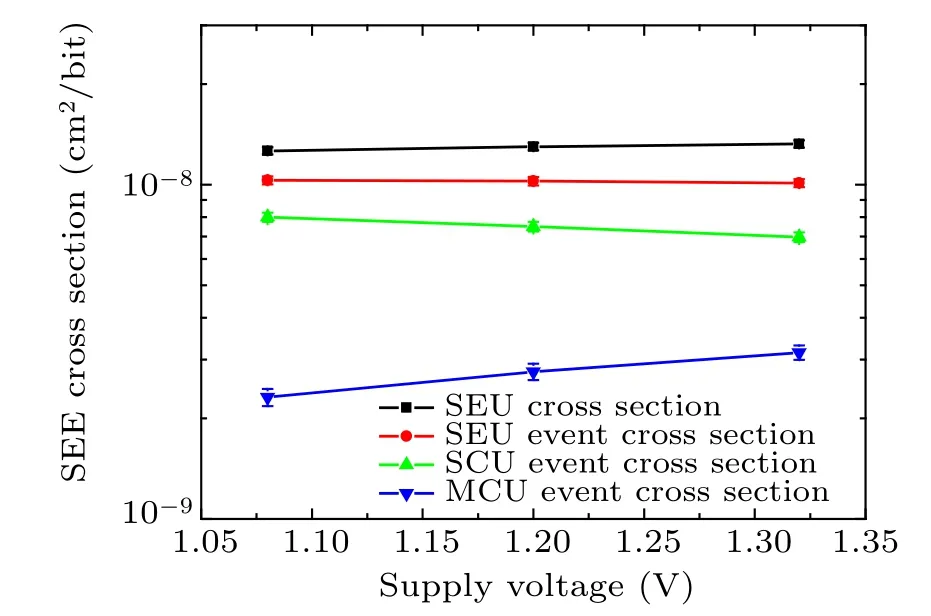
Fig.5. SEU,SEU event,SCU event,and MCU event cross sections versus supply voltage for 84.6 MeV·cm2/mg.
It can be seen that the SEU event cross section remains flat like the SEU cross section with the voltage scaling down. However, the SCU event cross section slightly increases, and the MCU event cross section slightly decreases.The MCU event cross section decreases by 1.36 times from 3.14×10?9cm2at 1.32 V to 2.31×10?9cm2at 1.08 V.The detailed analyses are given in the next section.
4. Analysis and discussion
4.1. Mecanism of MCU occurence
In order to reveal the mechanism of voltage influencing SEU and MCU,it is necessary to locate the positions of sensitive nodes in memory arrays through analyzing the layout information. Further,the topological pattern of MCU and the influence range of the incident ions can be acquired. Figure 6 shows the layout schematic diagram of adjacent six cells in the 6T SRAM.The contacts of n-well and p-well are placed within each memory cell in order to weaken the parasitic bipolar effect. A bit-interleaving layout technique is adopted to reduce the occurrence of MBU events. When the memory arrays are filled with all“0”or all“1”pattern,sensitive nodes of all the off-NMOS are adjacent vertically as well as horizontally,and sensitive nodes of all the off-PMOS are only adjacent vertically.
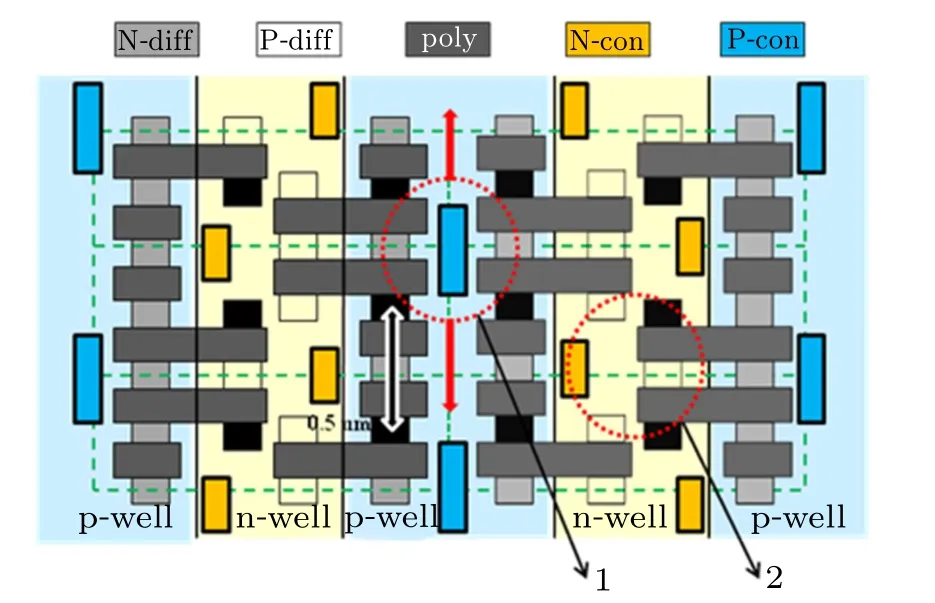
Fig.6. Layout schematic of standard 6T memory array including six cells.Black boxes are sensitive drains of off-NMOS and off-PMOS. Red dotted circles represent incident position of ions.
Figure 7 presents a subset of MCUs with different orders with various topological patterns during SEE testing. Each order MCU includes 1–3 kinds of patterns, the first of which is the major pattern and has the highest proportion. As shown in Fig.7, when the ions are incident normally, at most 2-bit MCU can be caused in the horizontal direction, while 4-bit MCU can be caused in the vertical direction. This means that the vertical MCUs along the well are more pronounced than those horizontal MCUs across the well. When the ion strikes the p-well (position No. 1 in Fig.6), the sensitive nodes of off-biased NMOS of adjacent memory cells share the same p-well. The radial track of the ion can simultaneously cover two cells in the horizontal direction, causing two cells to upset. In the vertical direction,charge diffusion along the p-well can be collected by multiple adjacent sensitive nodes,thus inducing the highest-order MCU8 with 4 rows×2 columns for 42 MeV·cm2/mg. If the ion hits the n-well (position No. 2),only one sensitive node of the off-biased PMOS is contained in the same n-well in the horizontal direction, so it is rare to cause horizontal double MCU. As a result, the MCUs with n rows×2 columns should mainly come from charge diffusion between adjacent NMOS transistors in the same p-well, and a small quantity of MCU with 4 rows × 1 column should be caused by charge sharing between PMOS transistors with the ions incident on n-well.[20]

Fig.7.A subset of MCUs with different orders with various topological patterns.
4.2. Influence mechanism of supply voltage on SEU and MCU
When the MCU is focused due to charge diffusion, the differences in SEU sensitivity among the different positions within a memory cell need to be considered. So the sensitive volume (SV) of memory cell is usually constructed as a nested structure composed of multiple sub-SVs with different charge collection efficiencies as shown in Fig.8. The central sub-SV with the highest charge collection efficiency is the center of the drain region of off-biased NMOS or PMOS,and the charges are collected mainly by drift process. The larger the area of the sub-SV,the longer the distance from the drain center is and the lower the corresponding charge collection efficiency. Charges produced by the incident ions are collected mainly through charge diffusion in these outer regions.The total collected charge quantity of SV is the weighted sum of the charges generated in each sub-SV.[21]The SEU can be caused when the collected charge quantity is greater than the critical charge quantity.
With the reduction of voltage,the critical charge quantity to trigger SEU also decreases. Reducing the voltage can also lower the electric field of the depletion region between the reverse biased drain-substrates. When the particles are incident on the center of drain region, the peak current will decrease and the delay time will increase during the charge collection.Eventually the total collected charges are almost the same at different voltages. So the charge collection efficiency of the central sub-SV almost keeps unchanged with the voltage variation under this circumstance.[23]But when the particles are incident on the outside of the drain region, the peak current due to drift is small,the lower voltage will increase the time of charge collection,resulting in more charge recombination during the diffusion process. So the charge collection efficiency of the outer sub-SVs will decrease with the reduction of voltage.

Fig.8. Nested SV structure composed of multiple sub-SVs with different charge collection efficiencies.[21,22]
When the 6T SRAM operates at 1.2 V,the LET threshold of SEU is around 0.28 MeV·cm2/mg in Fig.1. The thickness of the central sub-SV for low LET value is roughly equal to 350 nm which is the thickness of shallow trench isolation(STI). So the critical charge quantity is about 1 fC. For the low-energy protons,their LET value is 0.35 MeV·cm2/mg just exceeding the LET threshold of SEU.The SEU can be caused only when the particles are incident on the drain region. The influence of lowering the voltage on the critical charge is only focused on,not considering the impact on charge collection efficiency. Because the critical charge is generally proportional to the voltage,[24]the critical charge is around 1.1 fC when the SRAM operates at 1.32 V. In this case, only when the particles are incident on the center of the drain, can the generated charges be collected quickly to cause the SEU. As the critical charge decreases to about 0.9 fC with the voltage lowering to 1.08 V,even if the particles are incident on the edge of the drain center,a certain quantity of charges can also be collected to trigger the SEU.So the SEU cross section obviously increases even up to an order of magnitude. When the LET increases to 1.73 MeV·cm2/mg, the SEU cross section is approximately equal to the area of drain region,all the SEUs are still SCUs. Because the LET value is much higher than LET threshold of SEU, the generated charges are obviously more than the SEU critical charge at different voltages. Therefore,the influence of voltage variation on the SEU cross section becomes weakened.
The LET threshold of MCU is 2.8 MeV·cm2/mg in the 6T SRAM as indicated in Fig.1. Lowering the voltage will also reduce the LET threshold of MCU.[14]As the LET increases from 2.8 MeV·cm2/mg to the knee point of SEU cross section curve which is around 13.1 MeV·cm2/mg in Fig.1,the MCU mean,MCU ratio,and MCU event cross sections all increase with the voltage decreasing. But the SCU event cross section decreases, resulting in the decrease of the total SEU event cross section.Eventually,the SEU cross section remains unchanged with the voltage lowering when the LET value is above LET threshold of MCU.With the LET increasing above 13.1 MeV·cm2/mg,the MCU ratio in Table 2 reaches to about 60%. Because the LET value is far more than LET threshold of MCU,the influence of the difference in LET threshold of MCU due to voltage variation on MCU parameters can be weakened.
It should be noted that because the ion energy per nucleon is about 6 MeV/u in Table 1 and the maximum ion track radius is about 2 μm, the charge concentration is the highest in the center of ion track and decreases sharply with the increase of track radius.[25]When the heavy ion is incident on the position No. 1 in Fig.6, the spacings between sensitive nodes in the horizontal and vertical direction are both 0.5μm,four adjacent sensitive nodes can be covered by the ion track.Due to the small distance between the sensitive nodes and the center of ion track, four sensitive nodes can quickly collect enough charges by drift,[20]and MCU occurs. The effect of voltage variation on the LET threshold is dominant. When the LET values are 13.1 MeV·cm2/mg and 21.8 MeV·cm2/mg,LET threshold of MCU decreases with the reduction of voltage,leading the sum of MCU2–MCU4 event cross sections to increase. Because the LET value of 42 MeV·cm2/mg is much higher than the LET threshold of MCU at different voltages,voltage variation has little effect on the sum of MCU2–MCU4 event cross sections. For the MCU5–MCU8, the peripheral sensitive nodes are far from the center of ion track and mainly collect charges by diffusion. The sum of MCU5–MCU8 event cross sections decreases with lowering the voltage due to the reduction of charge collection efficiency of the outer sub-SVs for 13.1 MeV·cm2/mg and 21.8 MeV·cm2/mg,and has no obvious change for 42 MeV·cm2/mg because of the high LET value. But for the highest-order MCU event,the contribution of charge diffusion collection is maximum.With the reduction of voltage, the decrease in the charge collection efficiency of the outer sub-SV has an advantage over the decrease of LET threshold of MCU, resulting in the highest-order MCU event cross section decreasing.

Fig.9. Layout schematic diagram of double DICE radiation-hardened cells. Dotted circles represent incident position of ions.
Figure 9 shows the layout schematic of double DICE radiation-hardened cells. In order to minimize the parasitic bipolar amplification effect,N+guard rings are used as n-well contacts and intermittent P+ stripes are used as p-well contacts in the DICE SRAM.[26]Because all“1”are the worst test pattern for SEU than All “0” and logical checkerboard based on the layout analysis and SEU testing results,only the nodal spacing for different sensitive pairs with “1” stored in the memory cells is shown in Table 3. According to the Weibull fitting result of SEU cross section in Fig.3,the LET thresholds of SEU and MCU in DICE SRAM are about 21 MeV·cm2/mg and 64 MeV·cm2/mg, respectively. When the LET value is 42 MeV·cm2/mg, all the SEUs from the SCU and the SEU cross sections increase with the voltage lowering. Because the LET value is much higher than 21 MeV·cm2/mg, the influence of the voltage reduction on SEU cross section is relatively weak.

Table 3. Nodal spacings for different sensitive pairs with“1”stored in the memory cells.
It should be noted that the highest-order MCU8 with 42 MeV·cm2/mg appears as 4 rows ×2 columns in the 6T SRAM, which indicates that the maximum range influenced by the radial track of Br ions and diffusion length of charges is about 2μm along the p-well. For the double DICE device,the charge diffusion between NMOS sensitive pairs along the p-well is the main cause of SEU due to high mobility of electrons when the ions are incident normally.For the DICE A,the distance between AN1 and AN3 is 1.75μm and less than the influenced range of 2μm. So the SCU can occur in the DICE A when the Br ion with 42 MeV·cm2/mg is incident on position No. 1 in Fig.9. As the distance between BN3 of DICE B and AN1 of DICE A is 2.5 μm greater than the maximum range of 2 μm, Br ions cannot cause 2-bit MCU in DICE A and DICE B with the ions incident at position No. 2. When LET increases to 64.7 MeV·cm2/mg slightly higher than LET threshold of MCU which is about 64 MeV·cm2/mg, a very small amount of horizontal 2-bit MCU occurs. When the Ta ions with 84.6 MeV·cm2/mg are incident on position No.2,the ratio of MCU2 event is over 20%. It needs to be added that the highest MCU10 events with the topological pattern of 5 rows×2 columns occur in the 6T SRAM for 84.6 MeV·cm2/mg,no MCU5 events with 5 rows ×1 columns are found. This means that the influence range of Ta ion track and diffusion length in the p-well can reach 2.5 μm, thus causing MCU2 event in DICE SRAM. Because the LET of Ta ions is much higher than LET threshold of SEU, the influence of the voltage variation on SEU cross section in DICE SRAM can be neglected. However,the highest-order MCU2 event cross section which is also the total MCU event cross section slightly increases with the voltage increasing, which is similar to the characteristic of 6T SRAM.The increase of charge collection efficiency due to the increase of voltage has a slight advantage over the increase of LET threshold of MCU within a certain voltage, which makes it relatively easier for a small quantity of charges which diffuse farther to be collected by AN1/BN3,causing more 2-bit MCUs. Combining the increase of MCU event cross section with the decrease of SCU event cross section,the total SEU cross section and SEU event cross section are basically unchanged.
5. Conclusions
In this paper, the influences of lowering the supply voltage on SEU and MCU are investigated with different LET values ranging from 0.35 MeV·cm2/mg to 84.6 MeV·cm2/mg in two kinds of 65-nm SRAMs. No matter whether the SRAM is radiation-hardened SRAM or non-hardened SRAM,when all the SEUs are from the SCU, the SEU cross section increases with supply voltage decreasing. The lower the LET value,the more prominent the influence of reducing the voltage on SEU is. When the MCU begins to occur,the SEU cross section almost keeps unchanged with the voltage varying. The highestorder MCU event cross section decreases with the reduction of voltage due to the decrease of charge collection efficiency of the outer sub-SV.
With the feature size of devices scaling down for nanometer SRAM,the LET threshold of SEU and MCU will be both lower. It can be predicted that the LET range of heavy ions within which the reduction of supply voltage can affect cross sections of SEU and MCU event will decrease further. For the commercial off-the-shelf (COTS) non-hardened SRAMs which are often used in modern small satellites, the dependence of SEU on voltage vatiation should be considered for heavy ions with very low LET or the other particles with very low energy. This means that lowering the voltage may still be an available approach to reducing the power consumption through the optimization method of power supply in the actual space application of nanometer COTS SRAM.
猜你喜歡
Chinese Physics B(2023年11期)2023-12-02 09:23:06
Chinese Physics B(2022年11期)2022-11-21 09:39:22
Plasma Science and Technology(2022年2期)2022-03-10 03:49:46
Chinese Physics B(2021年10期)2021-10-28 07:01:10
瘋狂英語·讀寫版(2021年5期)2021-06-15 03:27:55
武漢科技大學(xué)學(xué)報(bào)(社會(huì)科學(xué)版)(2020年2期)2020-04-28 01:54:38
杰出人物(2020年2期)2020-04-01 15:20:22
河北醫(yī)科大學(xué)學(xué)報(bào)(2017年2期)2017-03-10 02:50:07
Transactions of Nanjing University of Aeronautics and Astronautics(2015年1期)2015-11-21 07:08:56
Transactions of Nanjing University of Aeronautics and Astronautics(2015年5期)2015-02-09 06:08:47
- Chinese Physics B的其它文章
- Quantum annealing for semi-supervised learning
- Taking tomographic measurements for photonic qubits 88 ns before they are created*
- First principles study of behavior of helium at Fe(110)–graphene interface?
- Instability of single-walled carbon nanotubes conveying Jeffrey fluid?
- Relationship between manifold smoothness and adversarial vulnerability in deep learning with local errors?
- Weak-focused acoustic vortex generated by a focused ring array of planar transducers and its application in large-scale rotational object manipulation?