
Novel lateral insulated gate bipolar transistor on SOI substrate for optimizing hot-carrier degradation
2014-09-06 10:49:41HuangTingtingLiuSiyangSunWeifengZhangChunwei
Huang Tingting Liu Siyang Sun Weifeng Zhang Chunwei
(National ASIC System Engineering Research Center, Southeast University, Nanjing 210096, China)
?
Novel lateral insulated gate bipolar transistor on SOI substrate for optimizing hot-carrier degradation
Huang Tingting Liu Siyang Sun Weifeng Zhang Chunwei
(National ASIC System Engineering Research Center, Southeast University, Nanjing 210096, China)
A novel lateral insulated gate bipolar transistor on a silicon-on-insulator substrate (SOI-LIGBT) with a special low-doped P-well structure is proposed. The P-well structure is added to attach the P-body under the channel, so as to reduce the linear anode current degradation without additional process. The influence of the length and depth of the P-well on the hot-carrier (HC) reliability of the SOI-LIGBT is studied. With the increase in the length of the P-well, the perpendicular electric field peak and the impact ionization peak diminish, resulting in the reduction of the hot-carrier degradation. In addition, the impact ionization will be weakened with the increase in the depth of the P-well, which also makes the hot-carrier degradation decrease. Considering the effect of the low-doped P-well and the process windows, the length and depth of the P-well are both chosen as 2 μm.
lateral insulated gate bipolar transistor(LIGBT); silicon-on-insulator (SOI); hot-carrier effect (HCE); optimization
The lateral insulated gate bipolar transistor (LIGBT) is the suitable device for the power integrated circuits (ICs) due to its capability of handling high voltage and heavy current and its compatibility with the standard CMOS process. The silicon on insulator (SOI) substrate can offer true dielectric isolation for power devices, which eases the integration of power devices and low voltage logic devices in power ICs. As a result, the SOI-LIGBT begins to be a promising device for power applications.
One typical application of the SOI-LIGBT (M1) is used as the high-voltage output stage in the plasma display panels (PDP) scan driver ICs[1-5]. During the working conditions, M1 will suffer from high voltage at “off-state” and heavy current at “on-state”. Therefore, the hot-carrier effect (HCE) becomes serious. So, the hot-carrier degradation of the SOI-LIGBT devices is one of the most important reliability issues in ICs.
The HC reliability of the SOI-LIGBT devices is becoming more and more important, but the in-depth study on the hot-carrier degradation mechanism of the SOI-LIGBT devices is less documented due to the complexity of its two kinds of carriers. Recently, to our knowledge, no studies have been focused on the structure optimization of these devices to decrease the hot-carrier degradation[6-8].
In this paper, to reduce the electric field and the degradation of the electrical parameters, a novel SOI-LIGBT is proposed with a low-doped p-type well (P-well) attached to the P-body under the channel region. It can be compatible with low-voltage CMOS processes completely without any additional mask. The length and depth of the P-well are varied and their effects on the degradation are investigated by using the T-CAD simulator and the charge pumping (CP) technique, which well support the experimental findings.
1 Device Structure and Experiment
The schematic cross section of the investigated SOI-LIGBT device in this paper is shown in Fig.1(a), and the fabrication of the device is implemented in the 0.5 μm complementary MOS technology and the SOI technology. The structural parameters are given as follows: the length of the polygate is 5 μm; the accumulation region length is 2 μm; the buried oxide thickness is 1.5 μm; the thickness of the silicon film above the buried oxide is 6.5 μm. The threshold voltage and the off-state BV are 1.1 V and 230 V, respectively. The special P-well structure is added to attach the P-body under the channel so as to reduce the hot-carrier-induced degradation. Moreover, it is noted that the concentration of the proposed P-well is much lower than that of the P-body. The concentration of the proposed P-well is 3×1012cm-2. The SEM image of the cathode region in the improved SOI-LIGBT can also be seen in Fig.1(b). The lengthLand depthDof the low-doped P-well are varied to obtain their effects on the hot-carrier degradation.
2 Discussions and Optimization
2.1 Experiment
The current in the SOI-LIGBT is composed of the electron current along the surface of the device and the hole current in the body of the silicon film above the buried oxide. The hole current is collected by the P+of the cathode, so the hole carriers generated from the impact ionization will be submerged into the large operation current of the SOI-LIGBT. Hence, the hole carriers cannot be detected. Therefore, the maximum substrate current cannot reflect the degradation level of the SOI-LIGBT device[9]. In this paper, the hot-carrier stress condition ofVgc=2.5 V andVac=165 V is selected at the maximum substrate current of the SOI-LDMOS device, which fully owns the same structures except for the doping type in the anode area compared with the novel SOI-LIGBT. During the experiments,Ialin(measured atVgc=5 V andVac=1 V) is monitored continuously to analyze the physical degradation. All the measurements in our experiments are performed at room temperature.
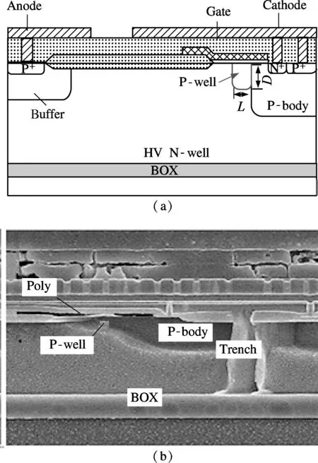
Fig.1 Schematic diagram of the proposed SOI-LIGBT device. (a) Schematic cross section; (b) SEM image of the cathode region in the proposed device
Before the hot-carrier degradation of the novel SOI-LIGBT is discussed, the influence of the added P-well on the electrical parameters of the SOI-LIGBT, such as the on-resistance, must be considered carefully. Actually, when the high gate operation voltage (7.8 V) is applied, the resistance of the P-well region will be much smaller than that of the added P-body region due to much more induced electron. Furthermore, it is the resistance of the HVN-well that will dominate the whole resistance of the device due to the long distance and the low doping. Therefore, the resistance of the added P-well region can be ignored compared with that of the P-body region and the HVN-well region. That is to say, the added P-well will not obviously impact the whole resistance of the device. The measuredI-Vcharacteristics of the novel SOI-LIGBT and the conventional one underVgc=7.8 V are shown in Fig.2. There is a little difference between them. And the key parameters of the two devices are shown in Tab.1.
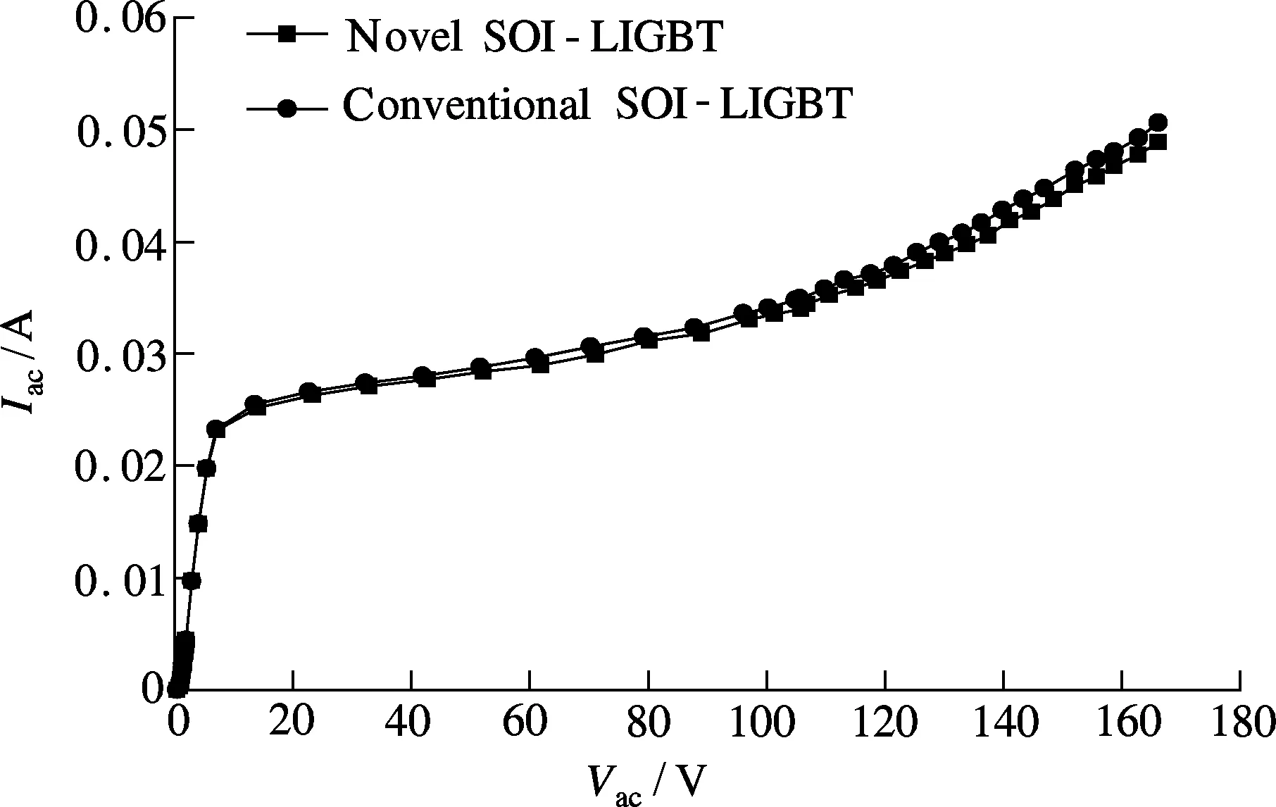
Fig.2 I-Vcharacteristics of novel SOI-LIGBT and conventional one
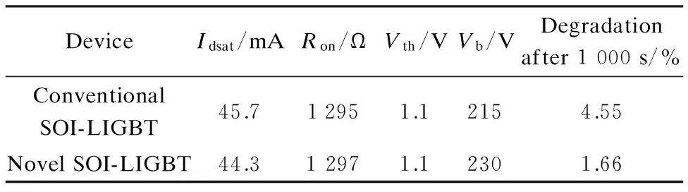
DeviceIdsat/mARon/ΩVth/VVb/VDegradationafter1000s/%ConventionalSOI-LIGBT45.712951.12154.55NovelSOI-LIGBT44.312971.12301.66
Fig.3 shows the parameter variations of the SOI-LIGBT devices under the stress ofVgc=2.5 V andVac=165 V. It is noted that there is almost noVthshift, implying that no hot carriers inject into the channel region. TheIalinincreases with the increase in the stress time, which reveals that there are many hot holes injecting into the bird’s beak[10]and the degradation is serious. It can also be found that the low-doped P-well can relax the increasing tendency of theIalinand the hot carrier degradation. The longer and deeper the low doped P-well, the smaller theIalindegradation will be.
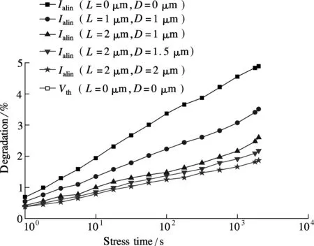
Fig.3 IalinandVthdegradation of the SOI-LIGBT devices with differentLandD
2.2 Influence ofL
In order to understand the above experimental results, The T-CAD simulations about the perpendicular electric field and the impact ionization are performed. Fig.4 and Fig.5 show the perpendicular electric field and the impact ionization along the Si/SiO2interface for the SOI-LIGBT with differentLandD=1 μm atVgc=2.5 V andVac=165 V. The first perpendicular electric field peak in the bird’s beak is negative (pointing to the oxide), which is helpful for the hot-hole injection, and the second perpendicular electric field peak in the channel region is positive, which is beneficial for the hot-electron injection. However, the impact ionization is mainly located in the bird’s beak and no obvious impact ionization can be observed in the channel region. As a result, a great amount of hot holes will be injected and trapped into the bird’s beak, resulting in the increase ofIalindue to the mirror induced negative charges. LessVthshift can be discovered due to no hot-electron injection in the channel region. In addition, according to Figs.4 and 5, it is observed that the increase of the length of the low-doped P-well will decrease the perpendicular electric field and the impact ionization in the bird’s beak. As a result, the hot-hole injection into the bird’s beak is diminished, and theIalindegradation turns much smaller.

Fig.4 Surface perpendicular fields with differentLandD=1 μm atVgc=2.5 V andVac=165 V
According to the influence ofLon the electric field and the impact ionization, one can know that the hot-hole injection and trapping into the bird’s beak can be reduced effectively by adjusting the dimension ofL. Although it is useful to increaseLfor hot carrier reliability, the dimension ofLcannot be greater than 2 μm in this case. Otherwise, it will exceed the accumulation region and lead to the abnormal threshold voltage, making the operation of the SOI-LIGBT abnormal. Considering the effect of the low-doped P-well and the process windows, we chooseLas 2 μm here. In this way, the hot carrier degradation of the SOI-LIGBT can be relaxed and its reliability can be optimized.
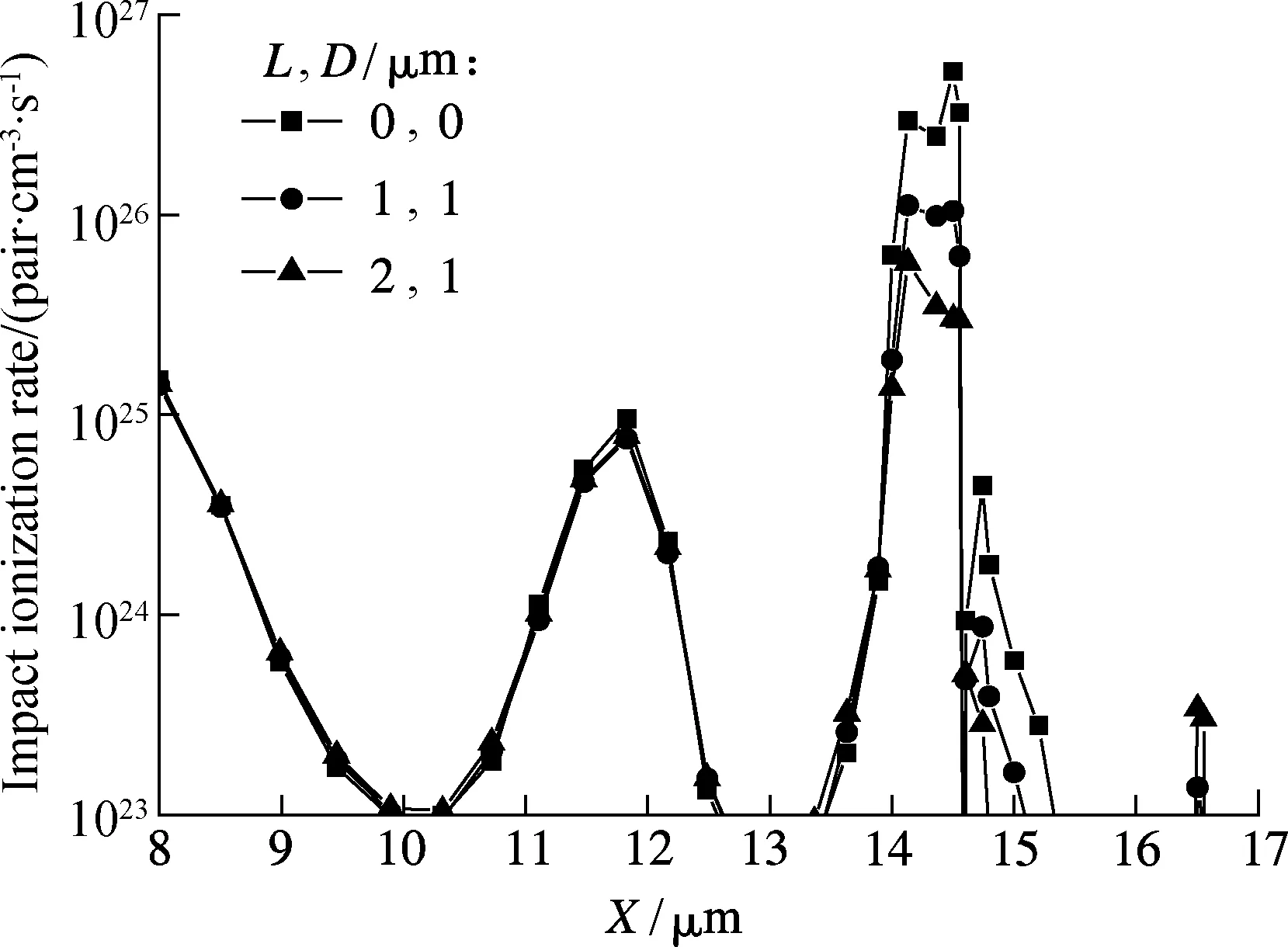
Fig.5 Surface impact ionization with differentLandD=1 μm atVgc=2.5 V andVac=165 V
2.3 Influence ofD
The influence of the depth of the low doped P-well on the impact ionization, which reveals the hot carrier degradation, is also simulated and compared in this paper. Fig.6 shows the 2D impact ionization of the proposed SOI-LIGBT with differentDand anLof 2 μm atVgc=2.5 V andVac=165 V. It is clear that the increase of the depth of the low doped P-well will decrease the impact ionization of the device, leading to the reduction of the hot carrier degradation. However, for the sameL, the value ofDcannot be too large. The reason is that during the production processes, the longtime annealing is used to obtain deepD, but at the same time it affects the value ofL. The longer the annealing time, the largerLandDwill be. The value ofLcannot be too large since the depth of the low doped P-well is limited. In this paper, the value ofDis chosen as 2 μm.
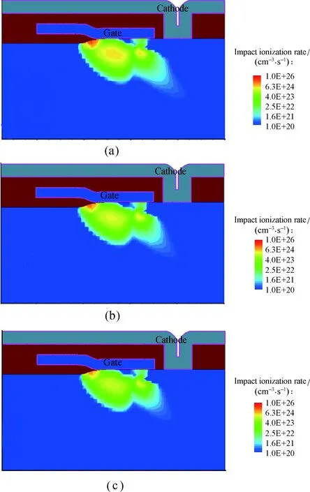
Fig.6 2D impact ionization of the proposed SOI-LIGBT with differentDatVgc=2.5 V andVac=165 V.(a)D=1μm andL=2μm;(b)D=1.5μm andL=2μm;(c)D=2μm andL=2μm
2.4 Charge pumping
In order to have a further understanding of the hot-carrier degradation of the SOI-LIGBT, the charge pumping (CP) technique is performed. The CP measurements are performed with the constant gate voltage pulse, whose amplitude and frequency are 10 V and 1 MHz, respectively. The base voltageVbaseof the pulse is varied from -15 to 5V. The rising and falling time of the pulse are both 100 ns. The anode and cathode are grounded. The CP currentIcpis measured from the substrate to reveal the hot-carrier trapping and the interface state generation. At the same time, theVgeandVgh(defined as the gate voltage to induce 1×1014cm-3electrons and holes, respectively) profiles of the SOI-LIGBT are shown in Fig.7 by using the T-CAD simulations. According to Fig.7,Icpcan be divided into three regions: the channel region (correspondingVbasefrom -5.5 (Vge-Vamplitude) to 0 V (Vgh) for the unstressed device), the accumulation region (correspondingVbasefrom -7.5 to -5 V for the unstressed device) and the field oxide region (correspondingVbasefrom -10 to -7.5 V for the unstressed device)[11-12]. TheIcpcurves of the conventional and proposed SOI-LIGBT (L=2 μm andD=2 μm) are measured and shown in Fig.8. The stress condition isVgc=2.5 V andVac=165 V for 2000 s. Comparing theIcpbefore and after the stress of the conventional device, it is clear that theIcpcurves shift left (change A), reflecting the hot hole injection into the bird’s beak. And the change of the value ofIcp(change B) indicates the interface state generation in the channel region, the accumulation region and the field oxide region. Moreover, it is also noted that the change A and change B of the proposed device are smaller than those of the conventional device after stress. That is to say, the hot-hole injection is restrained and the interface state generation is decreased in the proposed device. So the hot-carrier degradation for the SOI-LIGBT with the low-doped P-well is reduced.
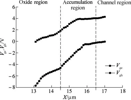
Fig.7 VgeandVghprofiles of the SOI-LIGBT
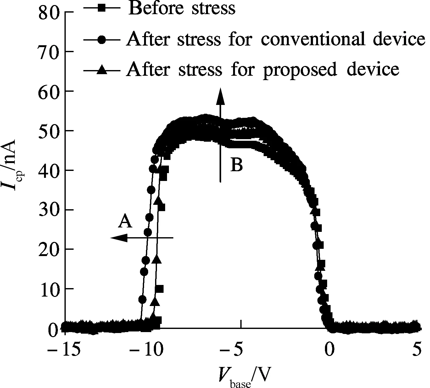
Fig.8 CP curves of the conventional and proposed devices before and after stress
3 Conclusion
A special P-well structure is added to attach the P-body under the channel in the SOI-LIGBT devices to reduce theIalindegradation without any additional mask. The special P-well is shown completely compatible with the low-voltage CMOS processes and does not impact the key parameters of the device. The influence of the length and depth of low doped P-well is studied in detail for the high-voltage SOI-LIGBT. With the increase ofL, the perpendicular electric field peak and the impact ionization peak diminish, resulting in the reduction of the hot carrier degradation. In addition, the impact ionization will be weakened with the increase in the depth of the low-doped P-well, which also makes the hot-carrier degradation decrease. Therefore, considering the effect of the low-doped P-well and the process windows, 2 μm is chosen for the length and depth of the P-well.
[1]Chen W S, Xie G, Zhang B, et al. New lateral IGBT with controlled anode on SOI substrate for PDP scan driver IC [C]//InternationalConferenceonCommunications,CircuitsandSystems. Milpitas, CA, USA, 2009: 628-630.
[2]Sumida H, Hirabayashi A, Kobayashi H. A high-voltage lateral IGBT with significantly improved ON-state characteristics on SOI for an advanced PDP scan driver IC [C]//IEEEInternationalSOIConferenceProceedings. Williamsburg, VA, USA, 2002: 64-65.
[3]Qiao M, Zhang B, Xiao Z Q, et al. High-voltage technology based on thin layer SOI for driving plasma display panels [C]//InternationalSymposiumonPowerSemiconductorDevicesandICs. Orlando, FL, USA, 2008: 52-55.
[4]Sun W F, Shi L X, Sun Z L, et al. High-voltage power IC technology with nVDMOS, RESURF pLDMOS, and novel level-shift circuit for PDP scan-driver IC [J].IEEETransactionsonElectronDevices, 2006, 53(4): 891-896.
[5]Tokumitsu S, Nitta T, Shiromoto T, et al. Enhancement of current drivability in field PMOS by optimized field plate [C]//InternationalSymposiumonPowerSemiconductorDevicesandICs. Hiroshima, Japan, 2010: 253-256.
[6]Wu H, Sun W F, Yi Y B, et al. Study and optimization of hot-carrier degradation in high voltage pledmos transistor with thick gate oxide [C]//InternationalSymposiumonthePhysicalandFailureAnalysisofIntegratedCircuits. Suzhou, China, 2009: 83-86.
[7]Bakeroot B, Doutreloigne J, Moens P. A new substrate current free nLIGBT for junction isolated technologies [C]//EuropeanSolid-StateDeviceResearchConference. Leuven, Belgium, 2004: 461-464.
[8]Lu D H, Mizushima T, Kitamura A, et al. Retrograded channel SOI LIGBTs with enhanced safe operating area[C]//InternationalSymposiumonPowerSemiconductorDevicesandICs. Orlando, FL, USA, 2008:32-35.
[9]Liu Siyang, Sun Weifeng, Qian Qinsong, et al. Comparisons of hot-carrier degradation behavior in SOI-LIGBT and SOI-LDMOS with different stress conditions [J].Solid-StateElectronics, 2010, 54(12): 1598-1601.
[10]Qian Q S, Sun W F, Liu S Y, et al. Novel hot-carrier degradation mechanisms in the lateral insulated-gate bipolar transistor on SOI substrate [J].IEEETransactionsonElectronDevices, 2011, 58(4):1158-1163.
[11]Moens P, Van Den Bosch G, Wojciechowski D, et al. Charge trapping effects and interface state generation in a 40 V lateral resurf pDMOS transistor [C]//EuropeanSolid-StateDeviceResearchConference. Grenoble, France, 2005:407-410.
[12]Heremans P, Witters J, Groeseneken G, et al. Analysis of the charge pumping technique and its applications for the evaluation of MOSFET degradation [J].IEEETransactionsonElectronDevices, 1989, 36(7): 1318-1335.
一種新型優(yōu)化熱載流子退化效應(yīng)的SOI-LIGBT
黃婷婷 劉斯揚(yáng) 孫偉鋒 張春偉
(東南大學(xué)國(guó)家ASIC系統(tǒng)工程技術(shù)研究中心, 南京 210096)
提出了一種新型絕緣體上硅橫向絕緣柵雙極型晶體管(SOI-LIGBT),該晶體管在溝道下方的P型體區(qū)旁增加了一個(gè)特殊的低摻雜P型阱區(qū),在不增加額外工藝的基礎(chǔ)上減小了器件線性區(qū)電流的退化.分析了低摻雜P阱的寬度和深度對(duì)SOI-LIGBT器件熱載流子可靠性的影響.通過(guò)增加低摻雜P型阱區(qū)的寬度,可以減小器件的縱向電場(chǎng)峰值和碰撞電離峰值,從而優(yōu)化器件的熱載流子效應(yīng).另外,增加低摻雜P型阱區(qū)的深度,也會(huì)減小器件內(nèi)部的碰撞電離率,從而減弱器件的熱載流子退化.結(jié)合低摻雜P型阱區(qū)的作用和工藝窗口大小的影響,確定低摻雜P型阱區(qū)的寬度和深度都為2 μm.
絕緣柵雙極型晶體管;絕緣體上硅;熱載流子效應(yīng);優(yōu)化
TN432
s:The National Natural Science Foundation of China (No.61204083), the Natural Science Foundation of Jiangsu Province (No.BK2011059), the Program for New Century Excellent Talents in University (No.NCET-10-0331).
:Huang Tingting, Liu Siyang, Sun Weifeng, et al.Novel lateral insulated gate bipolar transistor on SOI substrate for optimizing hot-carrier degradation[J].Journal of Southeast University (English Edition),2014,30(1):17-21.
10.3969/j.issn.1003-7985.2014.01.004
10.3969/j.issn.1003-7985.2014.01.004
Received 2013-08-06.
Biographies:Huang Tingting (1988—), female, graduate; Sun Weifeng (corresponding author), male, doctor, professor, swffrog@seu.edu.cn.
猜你喜歡
無(wú)線電工程(2024年9期)2024-10-24 00:00:00
云南師范大學(xué)學(xué)報(bào)(自然科學(xué)版)(2022年4期)2022-07-28 07:48:24
玩具世界(2022年1期)2022-06-05 07:42:20
大自然探索(2021年7期)2021-09-26 01:28:42
科技與創(chuàng)新(2016年16期)2016-09-23 11:30:40
實(shí)用臨床醫(yī)學(xué)(2016年8期)2016-06-08 06:10:16
電子器件(2015年5期)2015-12-29 08:42:07
發(fā)明與創(chuàng)新·大科技(2015年2期)2015-05-30 10:48:04
中國(guó)醫(yī)療器械信息(2015年10期)2015-04-13 04:08:06
電子設(shè)計(jì)工程(2014年18期)2014-02-27 12:00:26
 Journal of Southeast University(English Edition)2014年1期
- Journal of Southeast University(English Edition)的其它文章
- Wavelet transform and gradient direction based feature extraction method for off-line handwritten Tibetan letter recognition
- Analyses of unified congestion measures for interrupted traffic flow on urban roads
- Conditional autoregressive negative binomial model for analysis of crash count using Bayesian methods
- Design and analysis of traffic incident detection based on random forest
- Biodegradation of microcystin-RR and-LR by an indigenous bacterial strain MC-LTH11 isolated from Lake Taihu
- Inverse kinematic deriving and actuator control of Delta robot using symbolic computation technology