
Simulation of optical and electrical synaptic functions in MoS2/α-In2Se3 heterojunction memtransistors
2023-12-02 09:22:48TaoXiang相韜FengxiangChen陳鳳翔XiaoliLi李曉莉XiaodongWang王小東YulingYan閆譽玲andLishengWang汪禮勝
Chinese Physics B 2023年11期
關鍵詞:鳳翔
Tao Xiang(相韜), Fengxiang Chen(陳鳳翔), Xiaoli Li(李曉莉),Xiaodong Wang(王小東), Yuling Yan(閆譽玲), and Lisheng Wang(汪禮勝)
Department of Physics Science and Technology,School of Science,Wuhan University of Technology,Wuhan 430070,China
Keywords: α-In2Se3,MoS2,dual-gate control by electric and light,neural synaptic function simulation
1.Introduction
Due to the separation of the memory and processor and the serial instruction mode, computer systems based on von Neumann architecture have lower efficiency in large-scale and complex problems, especially in real-time visual and lingual processing.[1]Brain-inspired computing circuits with completely different structures and functions can enable highly efficient parallel computing making it easy to perform complicated tasks,which has attracted widespread interest and has become a research hotspot.In brain-inspired computing circuits, information is stored in multiple neurons that can simultaneously store and compute, thereby achieving efficient,distributed and parallel computing.[2]As the basic unit that completes the information transmission and coordination of brain neurons, synapse is also an important infrastructure for neural networks to learn, remember, and perceive other vital life activities.Thus, simulating neural synapses using electronic devices is the key to realizing artificial neural networks.As a result of continuously variable conductance,the memristor that can be successively switched between high-resistance state (HRS) and low-resistance state (LRS) are very suitable for neural synaptic applications.Furthermore,compared with memristors that only have two-terminal control, memtransistors combine the non-volatility of memristors and the gatetunability of transistors,which can achieve higher integration and more complex neural morphological learning.[3]
The two-dimensional (2D) material-based memtransistors have been demonstrated to be great potential synaptic components in brain-inspired computing circuits, with great prospects in efficiently executing intelligent tasks by complementing the von Neumann architecture.[4,5]Among them,MoS2has been widely studied due to its ultra-high stability,simple synthesis method, ultra-thin thickness, suitable band gap, high transparency, and tunability.Adithiet al.[6]built a memristor with MoS2prepared by chemical vapor deposition as the switching medium,which exhibited ultralow variability in synaptic weight update characteristics and could be integrated with neurons to realize logic gates.Jianget al.[7]constructed a novel electric-double-layer MoS2phototransistor with sodium alginate biopolymer electrolyte and performed electrical and optical synaptic simulations realizing photoelectronic and spatiotemporal four-dimensional hybrid integration.Another 2D materialα-In2Se3with both ferroelectricity and semiconductor properties could be polarized itself,which avoids the problems of depolarization field and leakage current of traditional ferroelectric materials.Moreover, due to direct band gap of multilayerα-In2Se3, its optical absorption ability in multilayer morphology precedes other transition metal dichalcogenides.Robinet al.[8]found far exceeded spectral responsivity and external quantum efficiency in anα-In2Se3photodetector compared with other layered semiconductors such as MoS2, GaS, and GaSe.Wanget al.[9]built anα-In2Se3ferroelectric semiconductor field-effect transistor device,which exhibited significant gate voltage controllability,well simulated the function of neural synapses, and achieved an accuracy of 91.9%in simulating artificial neural networks for digital image recognition.
In this article, an MoS2/α-In2Se3heterojunction memtransistor fabricated by mechanical exfoliation method is reported.Our fabricated device accomplishes type-II energy band arrangement in multilayer MoS2/α-In2Se3heterojunction,and thus achieves high response in optical measurements.In tests using electrical and optical pulses as input signals,the fabricated device can well simulate synaptic functions such as EPSC/IPSC,LTP/LTD,and PPF/PPD,and exhibits biologicallevel time constants,providing a possible solution for synaptic components in artificial neural networks.
2.Experiments
2.1.Sample fabrication
Multilayerα-In2Se3flake was mechanically exfoliated from anα-In2Se3bulk crystal and then dry-transferred to 100-nm thick SiO2/Si substrate.After that multilayer MoS2flake was selectively transferred onto the pre-selectedα-In2Se3to form a heterojunction,and the electrode pattern is customized by ultra-violet (UV) lithography, followed by deposition of a Cr/Au(5 nm/25 nm)film on the silicon substrate using thermal evaporation.Finally,the excess photoresist and metal were removed by lift-off process, resulting in the required electrode pattern and the construction of the MoS2/α-In2Se3heterojunction transistor structure.The prepared device structure is shown in Fig.1(a).
2.2.Electrical and optical characterizations
The morphology and composition of the device were measured by a JSM-IT800 field emission scanning electron microscope (SEM), a DI Nanoscope IV atomic force microscope (AFM), and an LabRAM HR Evolution Raman spectrometer,respectively.The transistor characteristics and electrical synaptic tests were performed on the device using a system composed of a Keithley 2636 and a probe station,while the optical synaptic tests were performed using a system composed of a Keithley 4200-SCS, a probe station, and a monochromatic light source.All tests were carried out at room temperature and under ambient conditions.
3.Results and discussion
3.1.Transistor characterization
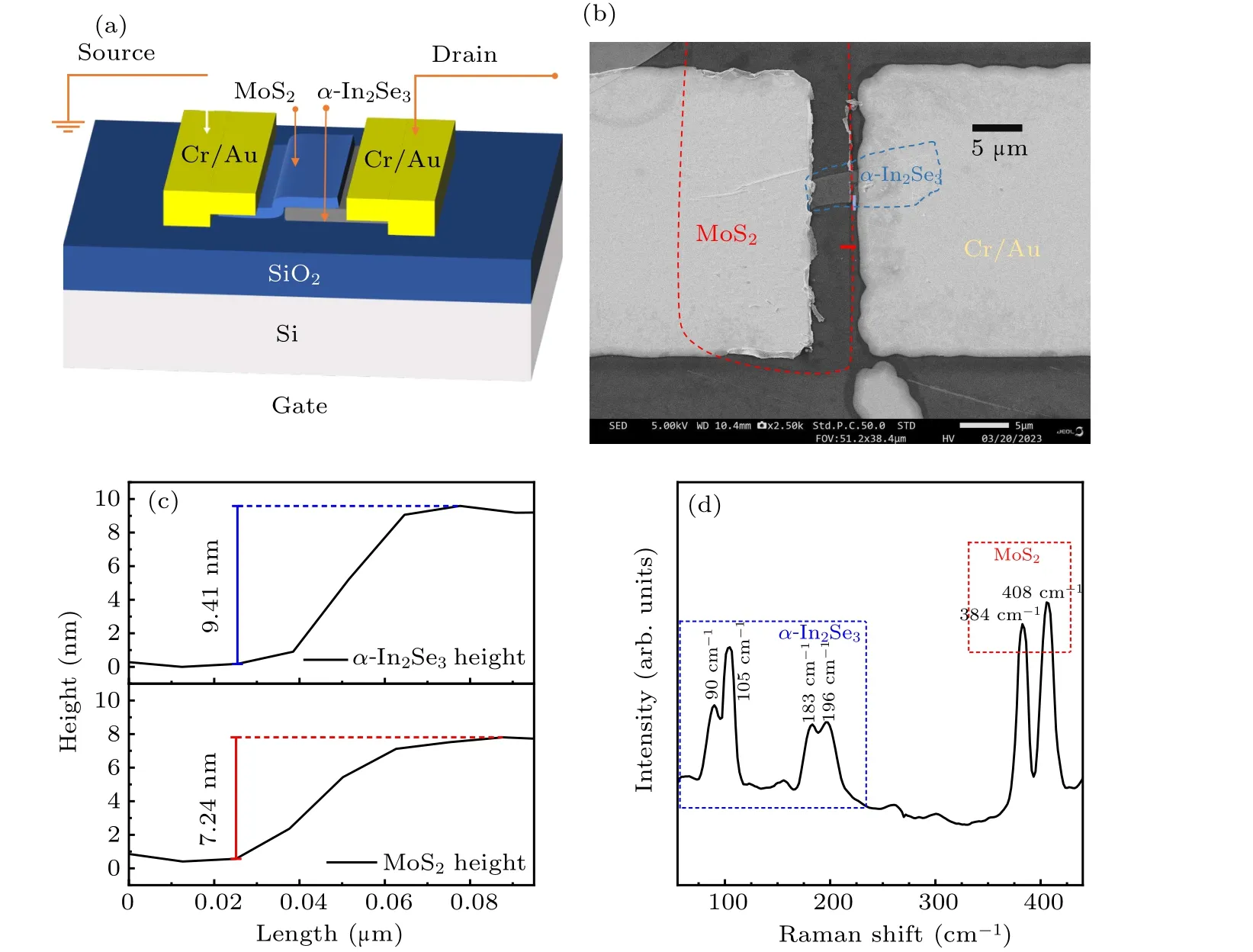
The morphology and composition measurement of MoS2/α-In2Se3heterojunction is shown in Figs.1(b)–1(d).As shown in Fig.1(b), SEM image showsα-In2Se3on the right side and MoS2on the left side marked by dashed line and Cr/Au electrodes on both sides.As shown in Fig.1(c),thickness profiles measured by AFM confirmed the thickness of 9.41 nm and 7.24 nm, which are approximately 9 layersα-In2Se3(1 nm per layer[10]) and 11 layers MoS2(0.65 nm per layer[7])corresponding to typical multilayer morphology.And,the measurement orientation ofα-In2Se3and MoS2are illustrated on the SEM by vertical short line and horizontal short line respectively.As shown in Fig.1(d), Raman spectra of MoS2/α-In2Se3heterojunction shows clear peaks on 90 cm-1, 105 cm-1, 183 cm-1, and 196 cm-1, which are slightly redshifted compared to the Raman results ofα-In2Se3with a thickness about 50 layers reported by Wanet al.[11]This fact keeps consistent well with research of Zhouet al.that the Raman peaks ofα-In2Se3are highly dependent on layer number.[12]In addition, Raman peaks also show two clear peaks at 384 cm-1and 408 cm-1corresponding to the inplane mode and out-of-plane mode of MoS2,respectively.[7]
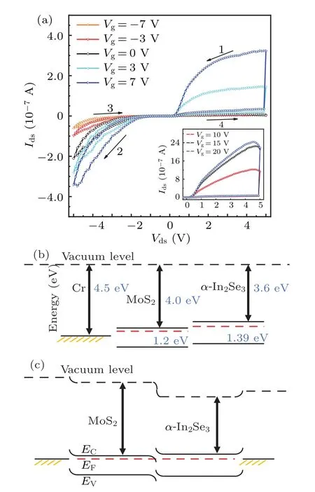
Due to suitable properties of MoS2andα-In2Se3, output characteristics of heterojunction memtransistor were first tested, as shown in Fig.2(a).If not specified, all tests were conducted in a dark,room temperature environment.The device was initialized with the drain–source voltageVdsscanned from 0 V to 5 V,and then scanned bidirectionally from 5 V to-5 V,while the gate voltageVgwas gradually increased from-20 V to 20 V.For ease of observation,only the output characteristic curves atVg=-7 V,-3 V,0 V,3 V,7 V are shown in the figure,and the output characteristic curves forVdsin the range of 0 V to 5 V atVg=10 V,15 V,20 V are shown in the inset, where the arrow in the figure indicates the direction ofIdswith the scanning voltage.After initialization, the device was in an LRS.During the process of scanningVdsfrom 5 V to-5 V,the device remains in the LRS and switches to an HRS at-5 V.It then remains in the HRS when theVdsis scanned back to +5 V.The device exhibits typical bipolar resistive switching behaviors.From the curve,as the gate voltageVgincreases from negative to 0 V,and then gradually becomes positive,the currentIdsin the device gradually increases with theVg, and the switching ratio also gradually increases.
To understand the hysteresis loop, a simplified energy band diagram before and after band bending is illustrated in Figs.2(b) and 2(c).According to the energy band diagrams, the Schottky barriers will be formed between MoS2and the electrode, as well as betweenα-In2Se3and the electrode.Generally, there are various defects in atomically thin MoS2, such as S vacancies, Mo–Mo dislocations,[13]and device preparation processes,such as photolithography and thermal evaporation, can also introduce some defects.These defects can form a large number of electronic trap states in the bandgap, which can capture or release charges during theVdsscanning process and adjust the height of the Schottky barriers.And thus, these trap states become the main factors affecting the hysteresis characteristics of the device under gate voltage modulation.Before initialization,the Schottky barrier formed between MoS2and the electrode is high and the device is in the HRS.WhenVdsgradually increases from 0 V to 5 V,electrons are injected from the source and captured by the trap states in MoS2until the saturation is reached, while the Schottky barrier is continuously lowered,leading the device to switch to an LRS.During process 1,in which theVdsscans from 5 V to 0 V,the device maintains LRS.In process 2, during theVdsscans from 0 V to-5 V,due to the applied negative bias,the trapped carriers are gradually extracted and the device switches from the LRS to the HRS.In process 3,the device maintains in the HRS asVdsscans from-5 V to 0 V.The process 4 is the same with the initialization process, and asVdsscans from 0 V to 5 V, the carrier injection causes the device to switch back to the LRS.
Next, the transfer characteristics were also tested to investigate the role ofα-In2Se3’s out-of-plane ferroelectricity on the device as shown in Fig.3(a).WithVdsfixed at 0.1 V,0.5 V,and 1 V sequentially,a bidirectional gate voltageVgscan from-10 V to 10 V was applied, and the change in currentIdsis indicated by the arrows, showing a clockwise hysteresis curve, which is consistent with the report of Siet al.[14]For transistor devices usingα-In2Se3as the channel material,if the gate oxide layer is too thick, the electric field across the semiconductor is not strong enough to penetrateα-In2Se3.Accordingly,only partial polarization switching happens near theα-In2Se3/SiO2interface,and the distribution of the polarization bound charges near the interface becomes an important factor affecting the channel resistance.
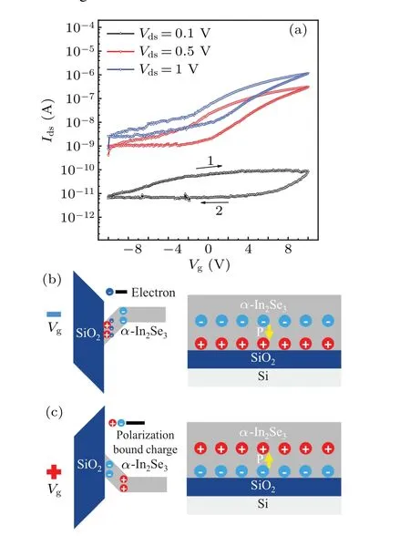
Figures 3(b)and 3(c)show the energy band diagram and the polarization bound charge distributions of the polarization down and up states ofα-In2Se3controlled by the gate voltage.For simplicity,the side ofα-In2Se3near SiO2is referred to here as the bottom surface(BS).A negativeVgleads to the polarization down state,mobile charges can accumulate at the BS because of the band bending, resulting in low channel resistance.Conversely,in the polarization up state introduced by a positiveVg,the mobile charge concentration at the BS is low,resulting in high channel resistance.WhenVgsweeps from-10 V to 0 V, the initial state has low channel conductance due to high negativeVg, whileα-In2Se3undergoes polarization down, leading to the generation of positive polarization bound charges on BS.As the gate voltage approaches to 0 V,the influence of gate voltage diminishes and the positive polarization bound charges will increase the electron concentration in the channel, and the device gradually switches to an LRS.WhenVgis scanned from 0 V to 10 V,α-In2Se3undergoes polarization up,while at this time the positiveVgdominates and the device maintains the LRS.During the process of sweeping back from 10 V to 0 V inVg,there is initially a high positiveVgand a high channel conductance,butα-In2Se3undergoes polarization up at the positiveVg, and the negative polarization bound charges are generated on BS,which will expel the electrons in the channel.So as the gate voltage sweeps towards 0 V,the influence of the gate voltage decreases,and the negative polarization bound charges ofα-In2Se3dominate,and the device switches to the HRS.During the scan ofVgfrom 0 V to-10 V,the device maintains the HRS,while the negativeVgwill cause a reversal polarization inα-In2Se3.
Besides the polarization ofα-In2Se3,considering the device preparation processes and the 100-nm SiO2gate oxide layer used, trap states, such as inherent defects in MoS2, defects introduced by fabricating processes, and the interface states between MoS2and SiO2, also have great influences on the transfer curves.[15–17]During the forward scanning(Vgscanning from-10 V to 10 V),the fixed trap states in MoS2released free electrons into the conduction band, which increased the carrier concentration, while during the backward scanning(Vgscanning from 10 V to-10 V),the free electrons would be captured leading to the carrier depletion.The carrier concentration eventually contributes to the clockwise hysteresis duringVgsweeping.The trapping-detrapping dynamics in MoS2and polarization inα-In2Se3jointly leads to a unique clockwise hysteresis curve in the MoS2/α-In2Se3memtransistor.
3.2.Synaptic function simulation
A distinct advantage of memtransistors for neurosynaptic applications over two-terminal memristors is the introduction of a new modulation mode,where the gate can simultaneously receive stimulation and read synapse weights.Since synaptic plasticity is very susceptible to environmental and historical activities,the synaptic plasticity of MoS2/α-In2Se3device has been explored systematically by applying electrical and optical pulses with various parameters.EPSC was simulated withVds=1 V,pulse width of 500 ms,andVg=-1 V,-3 V,-5 V,-7 V,-10 V sequentially.Each pulse is applied after the current from the previous pulse stabilizes.As shown in Fig.4(a), when a negative pulseVgis applied, the currentIdsimmediately produces a downward spike followed by an upward spike.This is due to the n-type semiconductor feature.The applied negativeVgreduces the carrier concentration in the channel, causing a downward spike in the current, while the negativeVgalso polarizesα-In2Se3downward, generating positive polarization bound charges on BS, which would substantially increase the carrier concentration in the channel,causing a subsequent upward current spike.
When the amplitude of the applied voltage pulse is too small,the polarization inα-In2Se3occurs only on the surface ofα-In2Se3near SiO2, and the polarization is not sufficient for significant potentiation in current,while when a large voltage pulse is applied, the polarization ofα-In2Se3deepens so that it has greater influence on the carrier concentration in the channel, leading to a larger post-synaptic current (PSC).After applying a-1 V pulse, the current gradually returns to its previous level over time.However, if the applied pulse voltage magnitude is greater than 3 V,it can be observed that the steady-state current in the device after the pulse ends is higher than the original current value.This indicates a transition from short-term memory (STM) to long-term memory(LTM),which is crucial for neuromorphic devices.The transition from STM to LTM is highly dependent on the gate oxide layer thickness,[9,14]and for the device fabricated in this article, a voltage amplitude greater than 3 V is necessary to observe an obvious transition from STM to LTM in EPSC.
In the subsequent IPSC testing, the polarity of the gate voltage is reversed thatVg=1 V,3 V,5 V,7 V,10 V with other parameters unchanged.Similar to the results of EPSC,Idshere produces an upward spike followed by a downward spike due to the generation of negative polarization bound charges at the BS.And the transition from STM to LTM can also be observed with increasing voltage amplitude.
As shown in Fig.4(b), LTP/LTD is measured with a series of potentiation pulse sequences followed by a series of suppression pulses.In the beginning, the LTP simulation was performed by applying a group of gate pulse sequences with a voltage amplitude of-10 V, duration of 500 ms, and 20 pulses.To obtain more stable current results,a waiting period of 20 s is allowed after each pulse before applying the next one.From Fig.4(b),it can be observed that the device’s current increases with each additional pulse, so that successive gate pulses modulation can achieve 20 consecutive conductance states in the channel.Next is the LTD simulation,
where the voltage amplitude is set to 6 V while keeping other parameters unchanged.The results show that continuous pulse sequences under positive voltage can also modulate the channel conductance continuously.Furthermore,a repetitive measurement with 8 consecutive LTP/LTD tests is performed as shown in Fig.4(c).Noticeably the device demonstrated good repeatability over 320 pulses and 6.4×10³s.
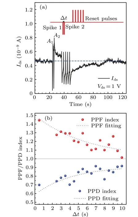
The PPF/PPD is an important factor of short-term synaptic plasticity, which manifests in the enhancement or inhibition of biological synaptic responses caused by two consecutive stimuli.[18]The schematic diagram of PPF measurement is shown in Fig.5(a), and PPF/PPD index with a fixedVdsof 1 V, the gate pulse voltage amplitude of 5 V, the pulse width of 500 ms, and increased time interval from 0.5 s to 10 s is plotted in Fig.5(b).To ensure the accuracy of the test, reset pulses with the same amplitude as the test pulse voltage but with opposite polarity is applied to the device after each test,and all PPF indices in this paper are calculated using
whereA1andA2are the amplitudes of the first and second pulse, respectively.The synaptic devices successfully simulate the PPF behavior of biological synapses and demonstrate the trend of the PPF index as a function of pulse interval between two consecutive light stimuli.According to the results,The PPF index of the device rapidly increases from 101% to 144% with decreasing the time interval from 10 s to 0.5 s.Note that the PPD index of the device decreases from 92%to 63%,indicating that the synaptic response is rapidly enhanced as the time interval decreases.In addition, the paired-pulse response in biological synapses can be simulated well by a parameterized single-exponential function.[19]In our device,the PPF/PPD indices were fitted using the following equation and the fitting curve was plotted in Fig.5(b):
where ?trepresents the time interval andτrepresents the time constant.The two characteristicτfor PPF and PPD are 6.03 s and 4.30 s,respectively,which are comparable to those measured in biological neural synapses.Combining the results of the above measurements on EPSC/IPSC, LTP/LTD,and PPF/PPD, it can be found that our device is capable of effectively emulating the various functions of synapses and has great potential for implementing neuromorphic computation, developing multifunctional and high-efficiency computing systems,as well as decoding temporal information and audiovisual signals.[19,20]
According to the energy band diagrams, the heterostructure of multilayer MoS2andα-In2Se3exhibits a type-II energy band arrangement.And the direct band gap ofα-In2Se3in multilayer morphology can significantly improve light absorption capacity and ensure fast response time.[21,22]Therefore, the conductance states in the channel are modulated by applying a 400-nm pulse to mimic the synaptic behaviors.The EPSC results withVdsof 1 V,pulse width of 500 ms and power densities of 33.0 μW/cm2, 80.2 μW/cm2, and 94.3 μW/cm2are shown in Fig.6(a).To ensure the result stability, a minimum waiting period of 30 s was introduced between each light pulse.The overall results ofI–tare shown in the upper part of Fig.6(a), where pulses with gradually increasing optical power were introduced at 28.8 s, 76.5 s, and 172.7 s, respectively.It can be seen that the PSC increases with the increasing optical power density.The lower part of Fig.6(a)shows a localized magnifiedI–timage to facilitate the observation of the PSC.It can be found that the device gradually transitions from STM to LTM with increasing light power,which is related to the trap capture of photo-generated carriers in the device.
During illumination, a large number of photo-generated electron-hole pairs will rapidly generate in the channel and the original Fermi level will split into quasi-Fermi levels for electrons and holes.After the light exposure ends,the quasi-Fermi levels will gradually recover to the equilibrium Fermi levels.Since a part of trapped electrons can be released by the traps in the channel,the photo-generated carriers will have a longer relaxation time and cannot drop to the initial states before illumination in a short time.[7,23]As indicated by the dashed lines in Fig.6(a), the current value extracted after a 30-s interval shows that there is no significant change in the current before and after the application of a 33.0-μW/cm2light pulse.Nevertheless,when pulses with higher power densities,for example,80.2 μW/cm2and 94.3 μW/cm2, are applied, the PSC in the device increases from 3.91×10⁻¹⁰A to 4.97×10⁻¹⁰A and 5.56×10⁻¹⁰A,respectively.Note that the PSC does not decay back to the resting current value,which indicates memory behaviors.
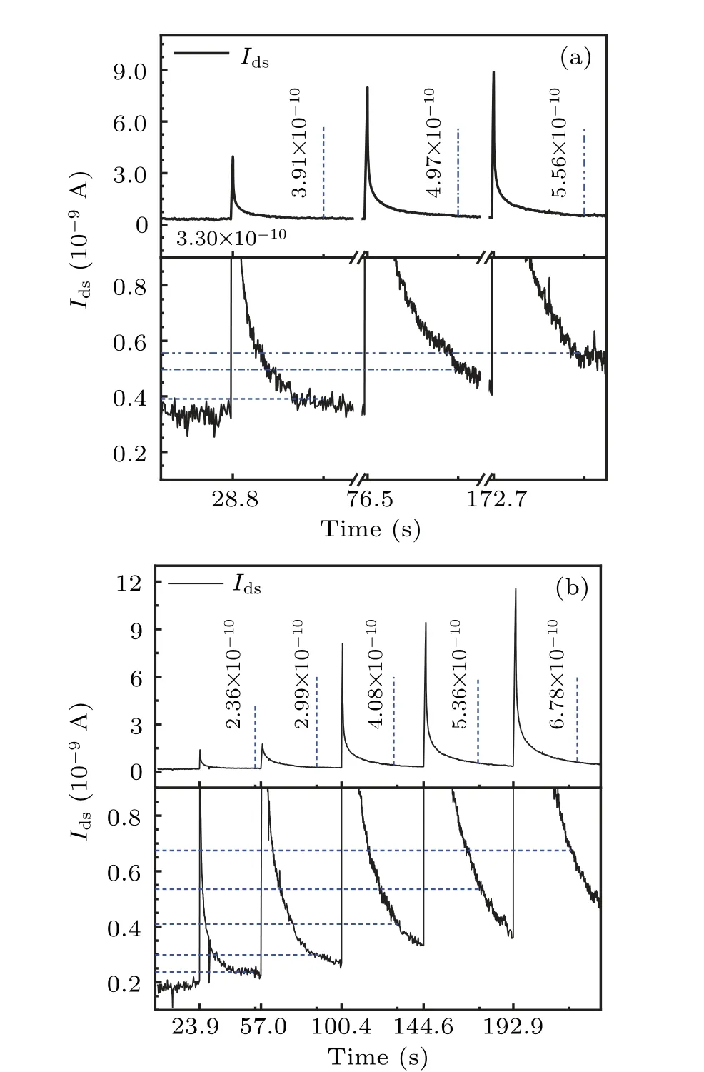

Figure 6(b)plots the EPSC results measured by applying a fixedVds(1 V) and various pulse widths of a single optical pulse (power density: 94.3 μW/cm2).The applied pulse widths are 100 ms,300 ms,500 ms,700 ms,and 1000 ms,sequentially.The upper part of Fig.6(b)presents the overallI–tcurve, demonstrating that the peak current increases with the pulse width.And the lower part of Fig.6(b)provides localized magnified results of the current within 30 s after each pulse.It can be seen that under the same power density, the wider the pulses,the higher the PSCs even after the equal waiting time.
Next, LTP measurements were performed as shown in Fig.7.To ensure the testing accuracy, the devices were kept in the dark for at least 2 minutes before each measurement.Figure 7(a) shows the LTP withVdsof 1 V, power densities of 33.0 μW/cm2and 94.3 μW/cm2, pulse width of 500 ms,and 10 pulses, which demonstrates that higher power density can modulate the device to higher conductance state.LTP with power density fixed to 94.3 μW/cm2, and pulse number changed to 5, 10, 15 or pulse width changed to 300 ms,500 ms, 700 ms are subsequently tested for comparison as shown in Figs.7(b) and 7(c).It can be seen that a greater number of pulses and wider pulse widths can also result in stronger responses of the optical synapse.As the pulse power density, pulse number, or pulse width increases, the PSC increases.The behavior is similar to that of brain functions of learning, remembering, and forgetting.As the number of learning increases, the memory is enhanced and hard to forget.The STM and LTM behaviors of synaptic devices are consistent with those of human visual synapses caused by light stimulation.
In Fig.8,two consecutive light pulses with a fixed pulse width(500 ms)and power density(94.3μW/cm2)are used to mimic the PPF behavior of the device by varying pulse intervals ranging from 0.1 s to 7 s.To ensure the testing accuracy,the devices were also kept in the dark for at least 2 minutes before each measurement.Figure 8(a) shows PPFI–tcurves for pulse intervals of 2 s and 0.5 s.When the first optical pulse is applied,a large number of photo-generated carriers are generated in the channel,causing a sharp increase in the current to reach a peak.Due to the relaxation time required for carrier recombination,the carrier concentration in the channel remains higher than the initial state.When the second pulse is applied,a current far exceeding the first peak is generated.It can be observed that for a time interval of 0.5 s, the increase in current exceeds even twice the magnitude compared to the case with 2-s interval.Figure 8(b)shows the PPF index calculated by Eq.(1) and the fitting results using Eq.(2).As the time interval decreases from 7 s to 0.1 s, the PPF index increases from 102%to 161%.By analyzing the fitting curve,the time constant of the device is determined to beτ=1.41 s,which is consistent with measurements of biological synapses,demonstrating that the device also has a significant potential for optical applications.The time constantτin optical PPF is relevantly small compared with electrical PPF’s,which is because of their different memory mechanisms.The time constantτcan reflect the time that the effect of the stimulus can exist,which is highly dependent on the memory mechanisms,[24]In electrical PPF/PPD, longerτof 6.03 s and 4.30 s were extracted due to the long retention time of the polarization,while in optical PPF, the higher rate of photogenerated carrier recombination leads to a shorter retention time, which causes a relatively short time constantτof 1.41 s.
4.Conclusions
In this paper, an MoS2/α-In2Se3heterojunction memtransistor was constructed on a heavily P-doped silicon wafer with a 100-nm SiO2layer using the micromechanical exfoliation method.It is demonstrated that the MoS2/α-In2Se3synaptic device can simulate the synaptic plasticity of biological synapses under different electrical and optical pulses.In measurements, electrical or optical pulses can enable transition from STM to LTM and modulate the device into different conductance states,corresponding to the learning,remembering, and forgetting behaviors of the human brain.So, our MoS2/α-In2Se3memtransistors have the potential for synapse simulation and provide a new option for synaptic components in artificial neural networks.
Acknowledgement
Project supported by the National Natural Science Foundation of China(Grant No.51702245).
猜你喜歡
Chinese Physics B(2022年12期)2022-12-28 09:55:28
當代陜西(2021年18期)2021-11-27 09:01:20
遼寧省博物館館刊(2020年0期)2020-08-13 09:15:54
中小學校長(2020年6期)2020-08-07 10:49:20
甘肅教育(2020年12期)2020-04-13 06:24:16
當代陜西(2019年23期)2020-01-06 12:17:42
藝術(shù)品鑒證.中國藝術(shù)金融(2018年8期)2019-01-14 01:14:56
當代陜西(2018年7期)2018-04-26 02:45:20
中國衛(wèi)生(2016年10期)2016-11-13 01:08:12
工業(yè)設計(2016年8期)2016-04-16 02:43:31

- Chinese Physics B的其它文章
- The application of quantum coherence as a resource
- Special breathing structures induced by bright solitons collision in a binary dipolar Bose–Einstein condensates
- Effect of short-term plasticity on working memory
- Directional-to-random transition of cell cluster migration
- Effect of mono-/divalent metal ions on the conductivity characteristics of DNA solutions transferring through a microfluidic channel
- Off-diagonal approach to the exact solution of quantum integrable systems