
Temperature dependence of single-event transients in SiGe heterojunction bipolar transistors for cryogenic applications
2023-10-11 07:56:32XiaoyuPan潘霄宇HongxiaGuo郭紅霞YahuiFeng馮亞輝YinongLiu劉以農(nóng)JinxinZhang張晉新JunFu付軍andGuofangYu喻國芳
Chinese Physics B 2023年9期
關(guān)鍵詞:紅霞
Xiaoyu Pan(潘霄宇), Hongxia Guo(郭紅霞), Yahui Feng(馮亞輝), Yinong Liu(劉以農(nóng)),Jinxin Zhang(張晉新), Jun Fu(付軍), and Guofang Yu(喻國芳)
1The Key Laboratory of Particle and Radiation Imaging,Ministry of Education,Department of Engineering Physics,Tsinghua University,Beijing 100084,China
2State Key Laboratory of Intense Pulsed Radiation Simulation and Effect,Northwest Institute of Nuclear Technology,Xi’an 710024,China
3School of Material Science and Engineering,Xiangtan University,Xiangtan 411105,China
4School of Aerospace Science and Technology,Xidian University,Xi’an 710126,China
5School of Integrated Circuits,Tsinghua University,Beijing 100084,China
Keywords: SiGe heterojunction bipolar transistors,pulsed laser,TCAD simulation,single-event transient
1.Introduction
Along with the continuous drive to explore deep space,how to save fuel consumption and enhance payload has been an important concern for scientists.Fortunately, silicongermanium heterojunction bipolar transistors (SiGe HBTs)with a wide operating temperature range and radiation resistance (even above the multi-Mrad total ionizing dose tolerance) make it possible to free electronic systems from the‘warm box’and reduce weight and energy consumption.Early SiGe prototypes are already flying in the International Space Station(ISS).[1]
However, SiGe devices are sensitive to single-event effects (SEEs), and effectively assessing their susceptibility to SEEs under extreme temperature conditions is still a critical issue that needs to be addressed.[2]According to existing research, there have been some valuable studies on the impacts of temperature on SEEs for different devices and ion types;for example, proton-induced SEU in SiGe digital logic,[3]the heavy ion- and pulsed laser-induced SET in a PIN Si epilayer,[4,5]and CMOS bulk technology over temperature.[6]This research has found that the dominant contributor to the temperature response is the variation of carrier mobility,with other factors neglected.The carrier mobility increases with decreasing temperature, which leads to higher transient amplitudes at cryogenic temperatures.However,the effect of incomplete ionization(hereafter abbreviated as i.i.)of impurities was not studied.
In the literature,[7]the inflection point (induced by the impurity’s incomplete ionization below 130 K) of the collector/substrate(C/S)junction’s transient peaks was found for the first time by TCAD simulation.However, there is no experimental evidence that the inflection point of transient peaks due to i.i.exists.What is more, the simulation LET is too small(only 0.01 pC/μm)to trigger the ions-hunt effect of the emitter/base/collector(E/B/C)stack,which is a common effect induced by space-heavy ions.[8]
In this work, we investigate the temperature dependence of the SET (especially the ion shunt effect when the initial electron-hole pairs’ (EHPs’) concentration exceeds the doping concentration of the intrinsic base)response in SiGe HBTs by two-dimensional(2D)raster scanning with a well-designed cryogenic test system suitable for pulsed-laser simulation.
There are two main innovations of this paper.Firstly,the increase in carrier mobility at low temperatures (which is well known already) and the i.i.of impurities (this work provides new experimental evidence)conjointly determine the change in resistivity on the charge-collection pathway, ultimately leading to variations of the drift transient peak.Secondly, when the device under test (DUT) switches from the cut-off state to the turn-on state (or the forward-active bias),there is a novel electron-injection process from the emitter to the base,which will increase the total charge collection.[2]An optimized built-in voltage equation of the high current compact model (HICUM)[9]has been provided with consideration of the i.i.The present experimental results illustrate that this novel injection process will be suppressed with decreasing temperature.According to existing research,this temperature dependence hasn’t been reported otherwise.More importantly, this work provides new evidence for the possibility of using SiGe HBTs at cryogenic temperatures outside the shielding‘warm box’.
2.Experimental and simulation details
2.1.Cryogenic system
As is well known,cryogenic temperature experiments are very difficult to conduct due to the long cooling times to reach a stable temperature and the need for a high vacuum environment to avoid frosting;[10]therefore, temperature-related experiments tend to be performed at temperatures near or above room temperature.When it comes to pulsed-laser experiments,things get even harder because of the very short working distance between the optical lens and the surface of the DUT (<1 cm).It is also important to note that even a very small amount of water vapor residue can have a significant impact on the accuracy of optical experiments.For these reasons, very few pulsed-laser studies have been performed for cryogenic temperatures.

Fig.1.The cryogenic system suitable for the pulsed-laser test contains(1)the laser system and the liquid nitrogen container; (2)a vacuum chamber with a hot and cold stage; (3) a vacuum pump; and (4) the precision temperature controller,liquid nitrogen cooling system,and the chillers.
Figure 1 shows the main components of our cryogenic system powered by INSTEC, which can provide a wide temperature range from-196°C to +200°C (with temperature stability better than±0.1°C).Before the experiment,the DUT was fixed directly on the silver stage with temperature sensors monitoring the real-time values.The vacuum pump usually requires 2–3 days(even longer)of continuous operation to remove most of the water vapor in the chamber,which is the key point for a laser test.
2.2.Radiation source
Nowadays, pulsed-laser systems are widely used as an important complement to high-energy ion accelerators for investigating SEEs.[11]This work was carried out at Northwest Institute of Nuclear Technology(NINT)by using the Nd:YAG laser system (powered by SPELS and EKSPLA), which can emit Gaussian laser beams with infra-red 1064 nm and visible 532 nm wavelengths.The single-photon energies of the 1064 nm laser and the 532 nm laser areEγ=1.17 eV andEγ=2.33 eV, respectively; both are above silicon’s bandgap(Eg= 1.12 eV) at room temperature to induce inter-band single-photon absorption (SPA).[12]The pulse repetition rate is 1 kHz.
Since the absorption coefficient(α)of the 1064 nm laser in silicon decreases sharply as the temperature decreases,[13]it is unsuitable to use 1064 nm laser light to simulate heavy ions at low temperatures.[14]Fortunately, the 532 nm laser’sαvaries little with temperature,so the EHPs’generation rate changes a little with temperature just like the heavy ion’s case.[15]In addition,the 1/e penetration length of the 532 nm laser beam is relatively short(about 1.25 μm),which makes it possible to focus on studying the ions-hunt effect of the HBT’s E/B/C stack without considering the drift transient component from the C/S junction.
2.3.DUT description
The DUT is a low noise NPN SiGe HBT designed by the School of Integrated Circuits, Tsinghua University.The lithographic node (or the emitter size) of the device is 0.4 μm×20 μm, which is configured by an interdigital chip layout with a 4E5B2C structure,as shown in Fig.2.Detailed information on the device is shown in Table 1.
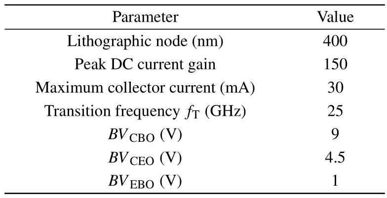
Table 1.Technology parameters of the DUT.
During the whole experiment, we kept the laser incident at the front side of the DUT for two main reasons: (1)decapping the backside package of the DUT can seriously affect its reliability;and(2)the 532 nm laser cannot penetrate the thick substrate layer to the sensitive volume.Since the sensitive area of the DUT is almost covered by a metal layer, only slits between the metal electrodes allow passage of the laser light into the semiconductor material.We selected a 50 μm×60 μm region,which covers all the sensitive volumes,and a 1 μm step size for the 2D raster measurements(in total,3111 data points)to reduce errors caused by fluctuations in laser incidence position and the metal layer’s blocking.The laser energy was fixed at 5 nJ to obtain more obvious transient signals that far exceed the testing noise floor.
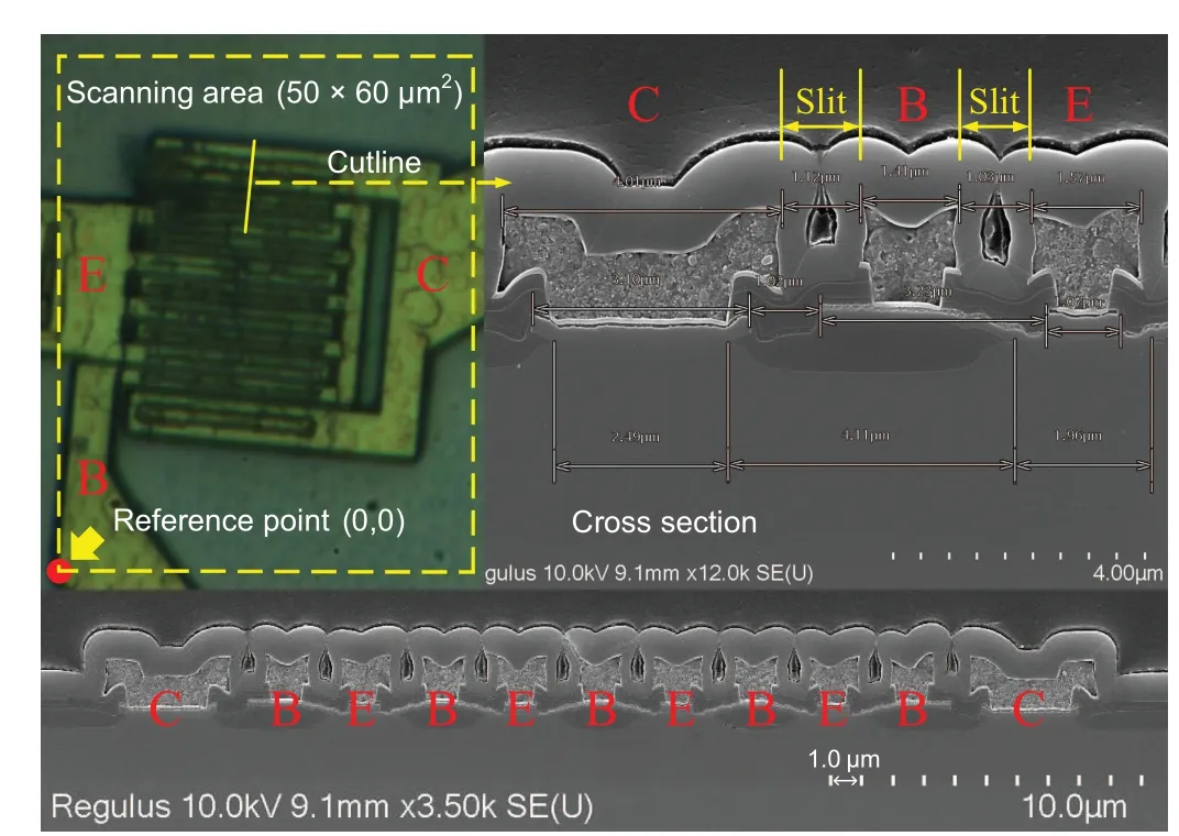
Fig.2.The chip layout of the DUT(left)shows the 2D raster scanning area and the SEM figure(right)shows a cross-section by the cutline.
2.4.The 2D TCAD process model
To qualitatively analyze the underlying physical mechanism, we built a well-calibrated 2D TCAD process model,as shown in Fig.3.One may notice that this is a simplified 1E2B2C structure,which gets better convergence at cryogenic temperatures,especially when the incomplete ionization model is activated(note that the convergence problem of threedimensional(3D)simulation at cryogenic temperatures has always been a stumbling block to be solved).The whole 3D process model is also shown in our previous study.[16]
When the ion-shunt effect of the HBT’s vertical E/B/C stack is triggered, a fast electron drift-collection process occurs from the emitter to the collector.Therefore, the resistance on this charge-collection pathway(shown in Fig.3)can be approximated as a series connection of the vertical E/B/C stack’s resistance(which includesRE,RB-V,andRC)and the lateral sub-collector’s resistance,RSC.In particular,theRB-Vmeans vertical intrinsic base resistance rather than the lateral resistance used in common compact models.Figure 4 plots the doping concentration at theY=0 μm cutline.
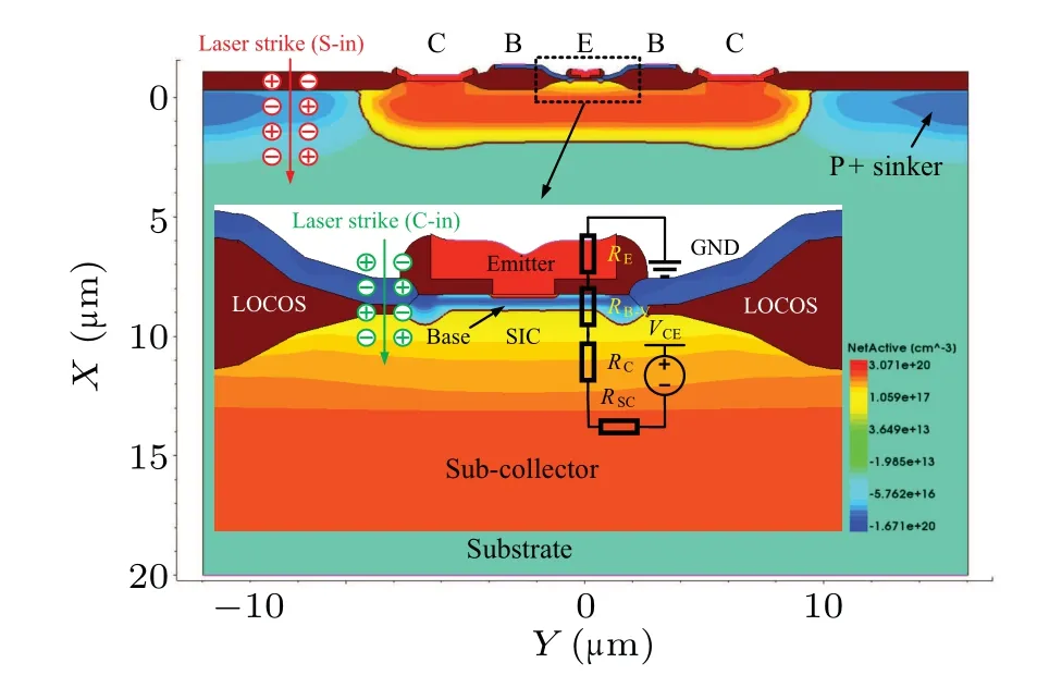
Fig.3.The 2D process model of the DUT,with a zoomed-in view of the inside that shows the parasitic resistance of the E/B/C stack.The different laser normal strike positions,marked with S-in,denote the substrate incidence,and C-in denotes close to the emitter center incidence.
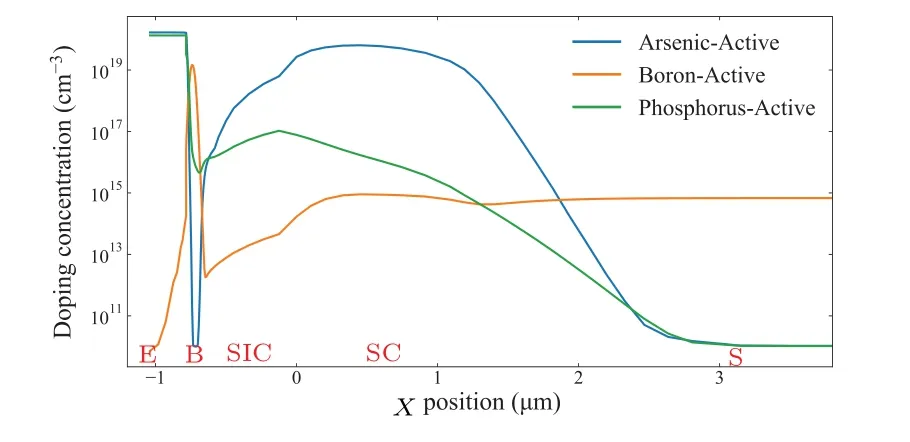
Fig.4.The doping concentration was extracted from the 2D process model at the Y =0 μm cutline.
2.5.Process simulation setup
To simulate the laser-induced SET, we introduced the SPA-induced EHPs’ distribution to the TCAD process simulation by using the analytical calculation methods shown in our previous study.[16]
There are some related papers on how to calculate the profiles of EHPs generated by a pulsed laser,[17–20]such as Eq.(1), which shows the EHPs’ generation rate at different positions:
whereαis the linear absorption coefficient,Teffis the effective transmission coefficient,ELis the pulsed-laser energy,Eγis the single-photon energy,randzare the radial and axial propagation distance, respectively,ωandω(z) are the 1/e2spot radius and contour after the wave has propagated a distance ofz,respectively,andτis the pulse duration.
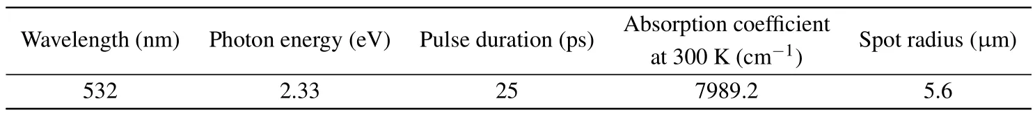
Table 2.Laser simulation parameters.
Note in particular that the 532 nm laser’s spot radius in Table 2 is 5.6 μm, which is far beyond the nominal value of 0.6 μm(given in Ref.[16]),and the reason is the presence of the 2 mm thick optical quartz window.As is shown in Fig.5,the quartz window could bring two unfavorable effects: (1)it slows down the convergence of the laser beam due to the law of light refraction;and(2)it makes the CCD camera view unclear.To maintain the consistency of the pulsed-laser experiments, we first adjusted theX–Y–Zpositioning platform in theZ-direction,so that the CCD camera could capture a relatively clear picture of the DUT’s layout.We were then able to compare theZ-coordinates with and without the quartz window to estimate the actual focus position and spot radius(ω)by optical calculations.[11]
Fortunately,the larger beam spot size does not affect the validity of this work because the sensitive area with the metal layer’s blocking is large enough (about 20 μm×20 μm, as shown in Fig.2) and contains repetitive 4E5B2C structures.Anyway, in the future, we will further optimize this issue by using thinner quartz windows(about 1 mm)and adding a focusing lens.
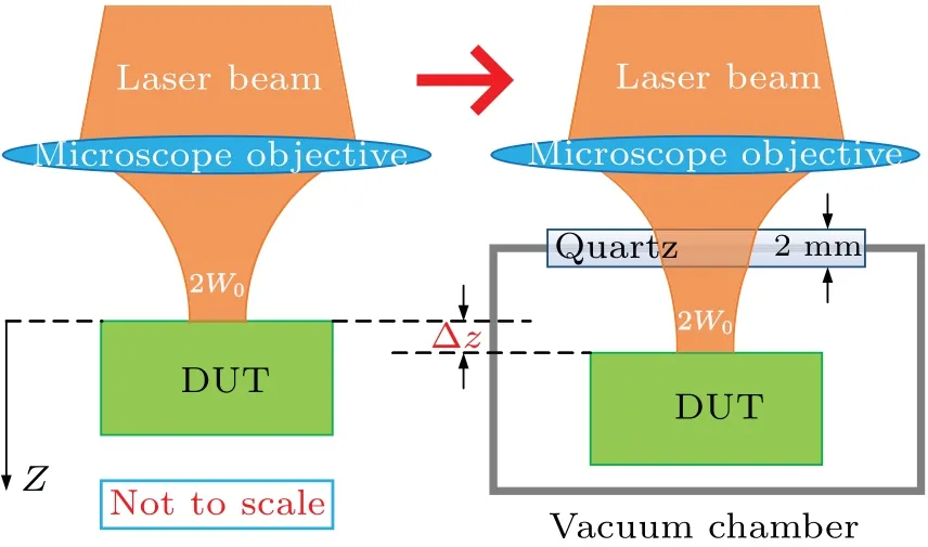
Fig.5.Laser path diagram with (right) and without (left) temperature control(note that the impact of the quartz window on the focus location is shown in Δz).
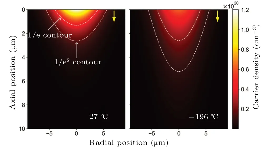
Fig.6.The 2D profiles for the 532 nm laser-induced EHPs at 27 °C(300 K)and-196 °C(77 K)with 5 nJ laser energy.The yellow arrows indicate the direction of laser incidence and the white dashed lines indicate the 1/e and 1/e2 contours of the carrier density.The absorption coefficients at different temperatures used here are extracted from Ref.[27].
Finally, according to Eq.(1), and taking into account the laser parameters mentioned above, we can plot the initial EHPs’profiles,shown in a colormap in Fig.6(Teff=1)).As we can see, variation of the absorption coefficientαwith temperature will slightly affect the initial carrier’s distribution(CD)while keeping the total amount constant.For simplicity,we adopted theαat 300 K to generate the initial CD profiles at all simulation temperature points.
We can then simulate the SPA-induced SET by modifying the heavy ion GCs’model parameters in TCAD.Our previous study[16]shows this process in detail.In addition, to simulate the carrier freeze-out,[21]we activated the Philips unified mobility model (PHUMOB),[22,23]Canali velocity saturation model,[24]Slotboom bandgap narrowing model,[25]and the incomplete ionization model.[26]
3.Temperature dependence of the transient peak
3.1.The 2D raster scan measurement
There are two main reasons for conducting 2D raster scan testing:(1)to obtain the SET sensitivity distribution of the entire chip; and (2) when averaging the waveforms in the same region,the influence of fluctuations in the metal layer’s blocking,and the laser incident position,the incident energy on the experimental results is reduced.
We set six temperature points at equal intervals (40°C)from+20°C to-180°C by using the cryogenic system mentioned in Subsection 2.1.We also changed the bias conditions of the DUT at each temperature point, including the on-state(withVCE=2 V,VBE=0.7 V)and off-state(withVCE=2 V,VBE=0 V).
After 2D raster measurements,we statistically calculated the transient peaks and collected charges (CCs) at 3111 laser incident points for each temperature, as shown in the colormaps of Figs.7 and 8.As can be seen, the presence of only one metal layer could also have a significant impact on SPA-induced transient peaks and CCs.The maximum values of both transient peaks and CCs are located in the area without a metal layer(the outside substrate region).
However, based on our previous studies,[16,28]the most sensitive volume for a SiGe HBT’s SET should be the central interdigital structure (especially the emitter center normal incidence) if there is no metal layer.Therefore, we divided the scanning area into the center-incidence(C-in)region(red boxes in Fig.7)and the substrate-incidence(S-in)region(white arrows in Fig.8).The definitions here are the same as in Fig.3.
In particular, the red boxes (10 μm×10 μm) in Fig.7 are the central parts of the 4B5E2C interdigital region(20 μm×20 μm) considering the large 5.6 μm laser-spot radius.We then calculated the mean values of the SET waveforms in the C-in and S-in regions.As an example, the offstate’s results are plotted in Fig.9.One can see that the transient peaks firstly increase with decreasing temperature(a maximum increment of about 25%),and then decrease slightly from-140°C to-180°C for the C-in case.In this region,the fast drift current dominates the SET waveform.
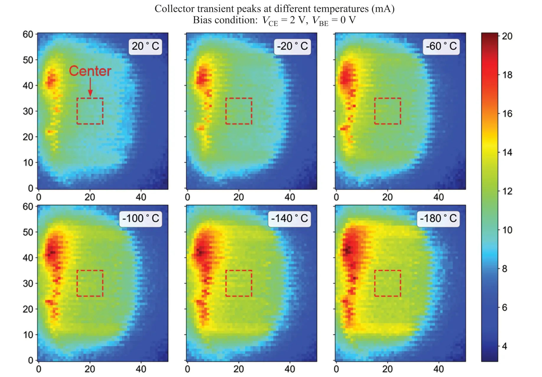
Fig.7.The 2D raster measurements for the collector transient peaks at different temperatures.The red box illustrates the center-incidence(close to the emitter center)of the 4E5B2C structure with the metal layer’s blocking.

Fig.8.The 2D raster measurements for the collector collected charges at different temperatures.The white arrows illustrate the substrateincidence(outside the 4E5B2C structure)positions without the metal layer’s blocking.
As a comparison,the transient peaks continue to slightly increase (a maximum increment of about 35%) for the S-in case because the dominant current is the diffusion current.For both cases, the full width at half maximum(FWHM)decreases with decreasing temperature and the total CCs show little change(as shown in Fig.10).What is more,we can obtain an estimate of the effective laser energy(0.15 nJ)and the surface LET value(28.37 pC/μm)of the C-in case.
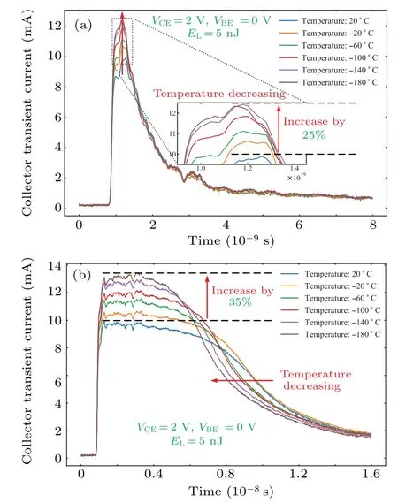
Fig.9.Mean waveforms for the collector’s SETs at different temperatures under (a) the C-in case and (b) the S-in case.The different time scales are shown right below.
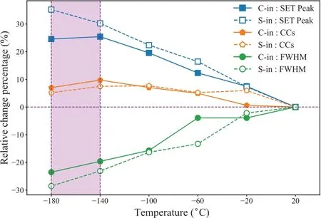
Fig.10.Relative percentage change (relative to 20 °C) on the collector’s SET peak,CCs,and FWHM under the C-in case and the S-in case(with VCE=2 V,VBE=0 V).
3.2.The 2D process simulation and analysis
In this paper,we have modified the TCAD parameter file of the heavy-ion model according to the analytical calculation results in Subsection 2.5 and have modified the simulation script file to simulate the pulsed laser penetrating a device structure based on the approach in our previous study.[16]
First, let us focus on the C-in case.Taking the transmission coefficient of the 2 mm thickness quartz window,the reflection of the DUT surface, and the blocking of the metal layer into account,we give a relatively rough estimated value of the effective transmission coefficient (in Subsection 2.5)based on the simulation results, hereTeff=0.1.[29]What is more, we have set the laser incidence position exactly to the emitter center normal incidence(the most sensitive volume).
It should be noted that it is difficult to find the real laser incidence position precisely.And considering that the high concentration of carrier profiles generated by the 5 nJ laser energy is sufficient to trigger the ion-shunt effect,these assumptions for the laser incidence position and effective transmission coefficientTeffare relatively reasonable,and do not affect the qualitative analysis and interpretation of the experimental phenomena in this paper.Figure 11 shows the SET simulation results in the off-state.The maximum value of the SET peak is around-160°C,which is 23.7%higher than 20°C and is similar to the testing results shown in Fig.9(a).The difference in FWHMs and durations between the simulation and experimental results come from the 2D simplified 1E2B2C simulation structure and the parasitic parameters from our testing system.

Fig.11.The C-in (emitter center normal incidence) SET waveforms from the TCAD simulation at different temperatures.
As mentioned before, many previous studies have attributed the temperature dependence of SET to carrier mobility.Carrier freeze-out at low temperatures doesn’t get enough attention.However, the TCAD simulation results in Ref.[7]have compared the SET’s temperature response with and without considering the i.i.at low temperatures.The peak inflection was only observed at the C/S junction’s transient component because the simulation LET is too small to trigger the ion-shunt effect.
The law of exponential variation of carrier mobility with temperature has been generally accepted for a long time.In the following, we focus on the i.i.of impurities at low temperatures.Taking the moderately doped intrinsic base as an example,we will introduce the ionization rate(IR)calculation process in detail.According to Altermatt’s i.i.model[30,31]and the optimized compact model by Luoet al.,[32]the impurity states could be divided into the always completely ionized free-states(with the share of 1-b)and partially ionized bound-states(with the share ofb),then the ionized acceptor’s concentration is shown below:
whereNAis the doping concentration,andf(EA)is the probability of the acceptor energy levelEAbeing occupied by electrons
withgA= 2 being a degeneracy factor for boron doping.Therefore,the IR with temperature could be found by
whereEV,EF, andEdopare, respectively, the valence band level,Fermi level,and the acceptor’s activation energy.

Fig.12.The ionization rate(unit: one)versus doping concentration at different temperatures for phosphorus,arsenic,and boron doping.
Detailed parameter settings and descriptions can be found in Refs.[30–32] and will not be presented here one by one.Finally, we calculated the three dopants’ ionization rates for the DUT, which are shown in Fig.12.We can see that i.i.could occur even at room temperature when the doping concentration is close to the Mott(metal–insulator)transition.[33]What is more, the ionization rate will decrease significantly when the temperature changes from-140°C to-180°C for both less than and close to the Mott transition.The peak doping concentrations in the base and the selectively implanted collector(SIC)are about 1×1019cm-3and less than 1×1018cm-3,respectively(from Fig.4),so these two moderate doping resistances(RB-VandRCin Fig.3)are dominated by both mobility and impurity IRs.For heavily doped regions(above 5×1019cm-3) like the emitter and sub-collector (or n+buried), the impurities are always completely ionized and the resistances (REandRSCin Fig.3) are controlled directly by the carrier mobility.
In addition,the SPA-induced high-density EHPs will also impact the local resistance on the charge-collection pathway because they can significantly change the free carriers’ concentration.Therefore, we need to calculate the resistivity by considering both the electrons’and holes’mobilities and concentrations by using
wherenandpare the electron and hole concentrations generated by both the intrinsic impurity’s ionization and the radiation-induced ionization, andμn,pare the electron and hole mobility, respectively.As shown in Fig.13, to qualitatively illustrate the relationship between the drift peak and resistivity, we extracted the resistivity values on the transient current pathway at the SET peak moments(around 20 ps)from the 2D process model.From-140°C to-180°C,RB-VandRCobviously increase andREandRSCslightly decrease.
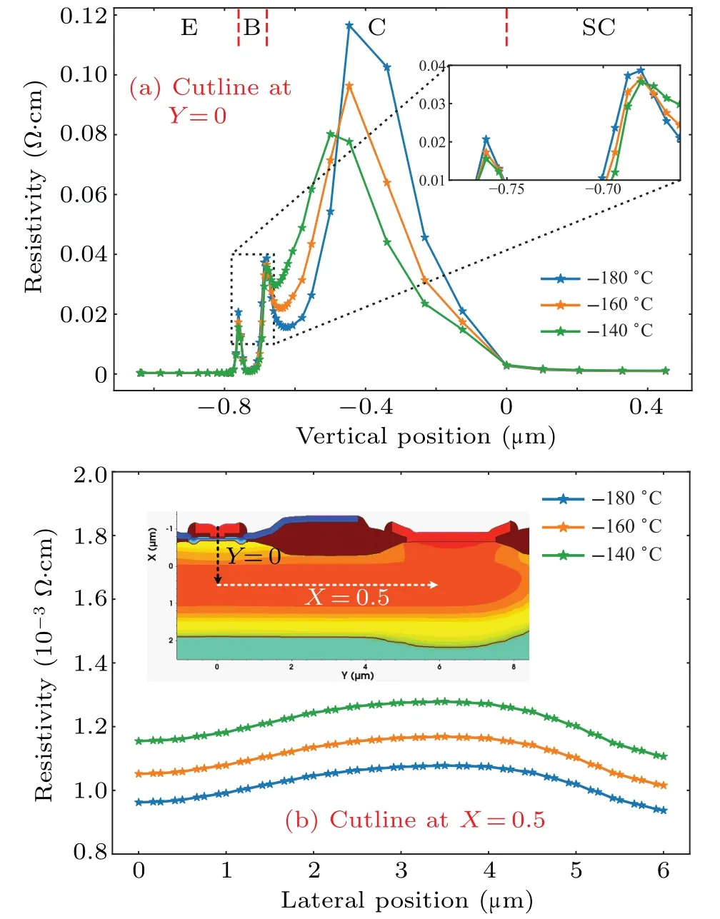
Fig.13.Variation of resistivity(at 20 ps)with temperature at different positions: (a)cutline at Y =0;(b)cutline at X =0.5.
Finally,we should also consider the structural dimensions of different regions on the E/B/C stack to obtain series resistance (details in Fig.3) other than resistivity.There are two competing mechanisms for the variation of the total series resistance with temperature:(1)the moderate doping base(RB-V) and lighter doping SIC (RC) with relatively high resistivities(which increase as temperature decreases)and very small vertical size; and (2) the heavy doping sub-collector(RSC) with lower resistivity (which drops along with temperature) and a much larger lateral size.In addition, the contribution of the emitter(RE)to the total series resistance can be considered negligible because of its low resistivity and small vertical size.
Taking into account these two competing mechanisms,it is not surprising to see a shift in the total resistance on the charge-collection pathway,which finally leads to an inflection point in the transient peak.In future work, the coupling between the 3D structure size and charge distribution needs to be fully considered in the calculation of series resistance.
Next, we discuss the S-in case (in Figs.3 and 8), which means that the pulsed laser strikes the outside substrate region without the metal layer.From the experimental results in Fig.9(b), we can see that the transient peak continues to slightly increase as the temperature decreases.The reason for this is that the SET current for substrate-incidence is mainly the diffusion current,which is dominated by the ambipolar diffusion coefficient(Da).For high-level injection(when EHPs’concentration is far beyond the background doping level,just like in this work),we could estimateDafrom the equation in Ref.[34].From the exponential increase of mobility with decreasing temperature, the carrier mobility’s variation will always dominate the bipolar-diffusion process.
4.Temperature dependence of the novel electron-injection process
4.1.Experimental and simulation results
During the 2D raster scan measurements,we also considered the impact of different bias conditions.We then found an important conclusion: that the novel electron injection from the emitter to the base will be suppressed at cryogenic temperatures.And this time,we will focus on the C-in case(emitter center strike)again.
By keeping all the experimental and simulation setups the same as in Section 3, we could obtain the collector transient currents with different bias conditions and temperatures,which are shown in Fig.14.The transient peaks for both the experimental and simulation results show a similar pattern of variation.When it comes to the total CCs, the simulation results have amplified the changes in the experiments.This deviation comes from the difference between the 2D simulation and the actual 3D device structure as well as the accuracy of the TCAD physical model.
Nevertheless, we can conclude that the transient peaks and CCs at low temperatures remain stable under different bias conditions.There will also be more electron injection from the emitter to the base when the temperature increases.

Fig.14.Variation of collector transient currents with temperature under different bias conditions: (a)experimental waveforms(note that,to show the differences between waveforms more clearly, the waveforms are artificially shifted in the time axis.); (b) TCAD simulation waveforms.Note that all DC components have been filtered out here.
4.2.Theoretical analysis
There are few studies on the bias condition dependence of a SiGe HBT’s SET.In the literature,[2]the conception of a‘novel collector-emitter diffusive component’was proposed after SET testing on a 9HP SiGe HBT.In this work, we call it the ‘novel electron-injection process from emitter to base’.It should be noted that the‘electron’here indicates the laserinduced free electrons at the emitter.The conduction band electrons generated by intrinsic impurity ionizing mainly produce the DC component,which has been filtered out here.
As is shown in Fig.15,this novel carrier injection is based on the principle that the positive bias voltage applied at the base lowers the potential barrier between the emitter and the base, thus allowing more electrons to cross (a diffusion-like process) the barrier layer to the base and eventually be collected by the collector terminal.Therefore, the temperature dependence of the E/B junction’s potential barrier will dominate this electron-diffusion process.
The built-in voltage(Vbi)of the E/B junction is dominated by the material’s lattice temperature and doping-dependent bandgap narrowing (BGN).[35]For silicon, the bandgap voltage (Vg) decreases as temperature increases, which could be described by Eq.(6)(from the HICUM model[9])
whereTis the nominal temperature 300 K(27°C),andk1=-0.025 V andk2=-0.053 V are constant parameters.

Fig.15.Novel carrier injection schematic.Note: the variation of the conduction band energy near the emitter-base junction with temperature and bias is extracted from the 2D TCAD simulation results.
Considering the i.i.(detailed in Subsection 3.2),we have then optimized the built-in voltage as
whereNDis the donor concentration(complete ionization due to the high doping level)of the emitter,NAis the ionized acceptor concentration of the base,VTis the thermal voltage(kT/q), andnieis the effective intrinsic carrier concentration by considering the BGN’s influence
Next, taking the i.i.into account, we could obtain the optimized built-in voltage in Eq.(9), and the last term shows the role of i.i.Eq.(10) illustrates the proportional relationship between the IR and ionized impurity concentration from Subsection 3.2.
It should be noted that the reference bandgap voltageVg(T0)=1.01 V is the average bandgap voltage of the emitter and the base,[9]by considering the impact of the Ge mole fraction.
Using the equations above, we could calculate the builtin voltages of the E/B junction at different temperatures, as shown in Fig.16.The built-in voltage of the E/B junction will increase as temperature decreases.And the simulation’s builtin barrier’s height is consistent with the analytical calculation results,which validate the effectiveness of our optimized builtin voltage calculation model.
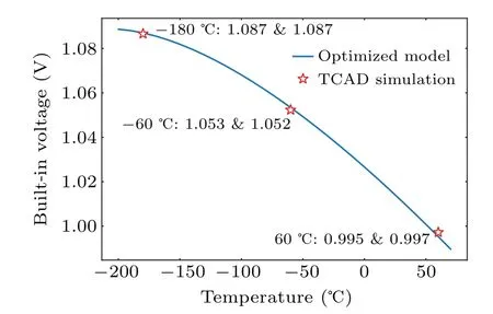
Fig.16.The built-in voltages of the E/B junction at different temperatures by using the optimized model calculation(blue line and font)and TCAD simulation(red symbols and font).
When the E/B bias is zero(VBE=0 V),one can see there is little electron injection from the emitter to the base because the potential barriers at the E/B junction remain at a high level at almost all temperature points.WhenVBE=0.7 V,this forward base bias could pull down the E/B barriers by about 0.7 V; at this point, the difference between the E/B barriers with different temperatures comes to the fore.Finally, more electrons are accepted(green arrows in Fig.15),injected from the emitter to the base at relatively higher temperatures due to the relatively lower barrier height.
In a word,our optimized built-in voltage model could extend the temperature range of the original HICUM model to extremely low temperatures.
5.Summary and conclusion
In this paper,the temperature dependence of single-event transients in SiGe HBTs was investigated.Comparing the experimental data and TCAD simulation results, we found that the variation of carrier mobility with temperature always plays a key role in SET peaks,and the impurity’s i.i.will also dominate and make an inflection point when it comes to cryogenic temperatures.These two factors together lead to a significant change in the resistivity of the intrinsic base region and the light-doped collector(both close to the Mott transition).What is more, the novel electron injection from the emitter to the base(when the transistor is in the on-state)will be significantly suppressed at cryogenic temperatures.This phenomenon is mainly due to the high emitter/base junction’s barrier heights at low temperatures.An optimized built-in voltage model is proposed to extend the original HICUM model to extremely low temperatures.The present work has provided new evidence for the adaptability and reliability of the SiGe HBT in cryogenic environments.
More work is necessary to improve the convergence of the 3D process simulation at cryogenic temperatures.The cryogenic experimental system needs to be further optimized, especially by thinning the thickness of the quartz window and adding focusing lenses as needed.What is more, we need to study a more accurate simulation method to extract the parasitic series resistance based on the 3D model.
Acknowledgements
The authors want to thank the contributions of the Institute of Microelectronics, Tsinghua University, for providing the DUT in this work.Sun Yabin and Fu Jun have also provided many valuable suggestions on the process simulation.Furthermore,the authors are very grateful to the engineers of SPELS and EKSPLA for their technical support in the daily use of the laser system.
Project supported by the National Natural Science Foundation of China(Grant Nos.61704127 and 11775167).
猜你喜歡
小學(xué)生作文(低年級適用)(2022年6期)2022-06-23 06:06:32
新高考·英語基礎(chǔ)(高一)(2022年3期)2022-04-29 05:06:32
小學(xué)生作文·小學(xué)低年級適用(2022年4期)2022-04-27 00:30:40
作文周刊·小學(xué)一年級版(2020年40期)2020-10-19 04:42:20
Journal of Acupuncture and Tuina Science(2020年4期)2020-08-29 02:49:54
大東方(2018年1期)2018-05-30 01:27:23
華南理工大學(xué)學(xué)報(bào)(自然科學(xué)版)(2017年4期)2017-06-19 18:25:50
作文周刊·小學(xué)一年級版(2016年28期)2017-06-03 00:28:49
中學(xué)生數(shù)理化·八年級物理人教版(2015年10期)2016-01-04 08:16:33
中國火炬(2014年7期)2014-07-24 14:21:26

- Chinese Physics B的其它文章
- Robustness of community networks against cascading failures with heterogeneous redistribution strategies
- Identifying multiple influential spreaders in complex networks based on spectral graph theory
- Self-similarity of complex networks under centrality-based node removal strategy
- Percolation transitions in edge-coupled interdependent networks with directed dependency links
- Important edge identification in complex networks based on local and global features
- Free running period affected by network structures of suprachiasmatic nucleus neurons exposed to constant light