
Demonstration and modeling of unipolar-carrier-conduction GaN Schottky-pn junction diode with low turn-on voltage
2023-03-13 09:20:04LijianGuo郭力健WeizongXu徐尉宗QiWei位祺XinghuaLiu劉興華TianyiLi李天義DongZhou周東FangfangRen任芳芳DunjunChen陳敦軍RongZhang張榮YoudouZheng鄭有炓andHaiLu陸海
Chinese Physics B 2023年2期
Lijian Guo(郭力健), Weizong Xu(徐尉宗), Qi Wei(位祺), Xinghua Liu(劉興華), Tianyi Li(李天義), Dong Zhou(周東),Fangfang Ren(任芳芳), Dunjun Chen(陳敦軍), Rong Zhang(張榮), Youdou Zheng(鄭有炓), and Hai Lu(陸海)
School of Electronic Science and Engineering,Collaborative Innovation Center of Advanced Microstructures,Nanjing University,Nanjing 210093,China
Keywords: GaN Schottky-pn junction diode(SPND),unipolar-carrier-conduction,low turn-on voltage
1.Introduction
Over the past decades, GaN has emerged as an attractive material for power devices owing to its advantageous material properties.[1,2]Growing efforts are now directed towards vertical devices,[2-4]considering their merits of achieving higher breakdown voltage and current levels without enlarging the chip size,[5,6]the superior dynamic switching performances,[7-9]and the relatively easier thermal management.[10]Among them,high-power and low-loss rectifying diodes are the fundamental devices for inverter/converter applications.From the perspectives of both the conduction loss and the switching loss, unipolar-operation Schottky barrier diode (SBD) is preferable to the bipolar pn diode (PND)for its low turn-on voltage and fast switching speed.[11-14]However, GaN SBD is faced with poor leakage blocking capability related to the interface located peak electric field under reverse bias, which could equivalently reduce the barrier thickness and facilitate the direct tunnelling process of electrons.[15]
In traditional Si and SiC power devices, junction barrier Schottky (JBS) diode has been developed as a solution,which under reverse bias utilizes the lateral depletion of locally doped p-islands to effectively enhance the barrier thickness underneath the Schottky junction, while under forward bias the JBS diode works like a conventional SBD.[16,17]However,the fabrication of the p-islands of the GaN JBS diodes requires additional complicated processing steps,e.g.,selectivearea ion implantation or regrowth of epilayer in the pre-etched grooves,which are still not commercially available and could induce non-negligible degradations in the material and interface quality.[18,19]
Alternatively,by adopting a sandwiched p-type layer between the Schottky metal and the n-type layer,the concept of the Schottky-pn junction diode(SPND)that has been proposed and applied in diamond and SiC power rectifiers could be a promising solution in the GaN power devices.[20-22]Based on the fully depletion of the sandwiched p-type layer, the electrons can diffuse and drift to the Schottky junction under positive bias without recombining with holes in the depleted p region.[20,23]Under reverse bias,the peak electric field located at the pn junction interface rather than the interface of metal and semiconductor could lead to an enhanced leakage blocking capability.However,corresponding design has rarely been investigated in the GaN, which could be a result of the immature technology of Schottky contact on the p-GaN layer,as well as the lack of a comprehensive model for the GaN SPND structure.
In this work,with the adoption of a 25 nm p-type inserted layer between the Schottky metal and the n-GaN layer,the first GaN SPND is demonstrated.Compared with the pn diode fabricated on the same GaN wafer,changing the anode structure on the p-GaN layer of the diode can evidently reduce the turnon voltage, leading to a more advantageous forward conduction capability.Clear unipolar carrier conduction characteristic of SPND is verified by the temperature-dependentI-Vtests and electroluminescence spectra.Correspondingly, an analysis model based on formulating the built-in potential (Vbi) of SPND has been presented, describing its dependence on the thickness and the doping concentration of the p-type layer,as well as the work function of the Schottky metals.Series of the GaN SPNDs with different Schottky metals, e.g., Ni, Au,Cr, and Ti, are fabricated for the verification of this model,
where near-ideal consistence is achieved between the calculation and experiment results.This work thus presents a novel design strategy for the vertical GaN diode based on the SPND configuration.
2.Experiments
The quasi-vertical GaN SPND and the control sample of GaN PND are fabricated on the same GaN wafer, as shown in Fig.1.The GaN epitaxial structure is grown by MOCVD on sapphire substrate and consists of a buffer layer, a 2 μm n+-GaN layer, a 8 μm n--GaN (n ≈1×1016cm-3), and a 25 nm p-GaN layer (Mg≈3×1019cm-3, the hole concentration (p) is determined as 4×1017cm-3by the Hall effect measurements using a monitor wafer).The beveled mesa structure is prepared by photolithography with photoresist reflow technique and inductively coupled plasma etching processes, as detailed in Ref.[24].Resultantly, a mesa with a 18°bevel angle is formed, which is followed by the treatment with tetramethyl ammonium hydroxide (TMAH)solution to remove the etching-related damages.The cathode electrodes of Ti/Al/Ni/Au (40 nm/80 nm/40 nm/120 nm) are deposited and treated with rapid thermal annealing (RTA) in N2at 850°C for the n-type ohmic contact of both SPND and PND.Circular Schottky electrodes of Ni/Au(100 nm/100 nm)with a diameter of 90μm are formed on the p-GaN layer for the SPND.On the other hand, the ohmic contacts of Ni/Au(20 nm/20 nm)are deposited on the p-GaN layer with the same diameter of 90μm for the PND.The ohmic contacts are later treated with RTA in air at 500°C for 10 min and covered by the metal pad of Ni/Au(100 nm/100 nm)for a better electrical contact.

Fig.1.Schematic cross-sections of (a) GaN SPND and (b) GaN PND fabricated on the same wafer.
3.Results and discussion
Figures 2(a) and 2(b) present the room-temperatureJ-Vcurves of the fabricated GaN SPND,and PND in semi-log and linear scale, respectively.Typical turning-on and -off performances of pn junction could be observed in the PND,featuring a rectifying ratio of~107and a turn-on voltage of 3.04 V(extracted at 1 A/cm2).The electroluminescence spectra of these diodes as normalized to the peak value at 365 nm of PND are presented in Fig.2(c).The strong GaN band-edge emission of 365 nm(3.4 eV)can only be observed in PND,which should be the result of the radiative recombination of electrons and holes under forward bias conditions,being consistent with the ideality factor of PND near 2, as shown in Fig.2(b).These results prove the good quality of the GaN epi-wafer and the pn junction.
SPND fabricated on the same wafer only changes the anode electrode in comparison with the PND.Apparently lowered turn-on voltage of 0.82 V (extracted at 1 A/cm2) is achieved in the SPND,which leads to a high forward current density of 700 A/cm2at 3 V, where the PND is still at off state,presenting advantageous forward conduction as obtained in the SPND.By assuming an operation condition with forward current of 1000 A/cm2, 45.6%reduction in the conduction power loss could be obtained with SPND.Meanwhile,an apparent variation in the ideality factor(n)could be observed with the application of the SPND structure,where the lowerednfrom 2.3 of PND to 1.48 clearly reveals the modified conduction characteristic from the bipolar pn junction.Moreover,no electroluminescence is observed on the SPND in contrast with the PND.It unveils the negligible radiative electron-hole recombination process under forward conduction and implies the single-carrier conduction characteristic.
Correspondingly, detailed analysis on the forward conduction of SPND has been performed.Given that the built-in potential of Ni/p-GaN contact is around 2.09 V-2.5 V,[25,26]the theoretical depletion depth of the Schottky barrier in p-GaN with a free carrier density of 4×1017cm-3could be calculated as 75 nm based on the Poisson’s equation.[27]This theoretical depletion thickness extends the thickness (25 nm)of the sandwiched p-type layer.Therefore, together with the depletion effect from the n--GaN layer,the sandwiched p-type GaN layer should have been fully depleted by the Schottky junction and the pn junction at the thermal equilibrium condition as shown in Fig.2(d).By increasing the forward bias for p/n-junction, the enhanced external electric field would offset the built-in electric fieldFPNas produced by p/n-junction and elevate theFSchottkyproduced by the Schottky junction.Resultantly,the space charge thickness of sandwiched p layer originating from the Schottky metal increases, whereas that from the p/n-junction decreases.Figure 2(e)presents the situation under forward bias,where the sandwiched p layer is completely depleted by the Schottky metal and a flat band is formed in the n--GaN layer.Electrons in the n--GaN layer,as driven by the forward voltage,could diffuse and drift to the Schottky metal through the depletion region directly,facilitating a single-carrier conduction process like SPNDs fabricated on diamond and SiC.While under the reverse bias condition as shown in Fig.2(f),the sandwiched p-type layer would keep the fully depletion state and contribute to the blocking of the reverse leakage.

Fig.2.Typical J-V characteristics of the GaN SPND and the PND:(a)in semi-log scale,(b)in linear-scale and ideality factor.(c)The electroluminescence spectra of SPND and PND.Insets of panel (c): the photograph of the fabricated PND (left) and its electroluminescence photograph (right).Schematic band diagrams of SPND at(d)thermal equilibrium condition,(e)forward bias condition,and(f)reverse bias condition.
Temperature-dependentJ-Vcharacterizations from RT to 398 K are conducted to obtain a more comprehensive understanding of the forward conduction characteristics of the SPND.In Fig.3(a), the turn-on voltage of SPND decreases with increasing temperature.As predicted in the Schottky theory, the thermionic emission (TE) model could describe the current flow when the ideality factor is closed to unity.In Fig.3(b),the fitted ideality factor decreases from 1.48 at room temperature to 1.18 at 398 K, implying the TE process dominates the SPND conduction at higher temperature.Then the forwardJ-Vcharacteristics could be given by[27-29]
whereJis the current density,kBis the Boltzmann constant,nis the ideality factor,Ris the series resistance,J0is the saturation current density,Tis the temperature,A?is the effective Richardson constant andqφBis the barrier height.Equation(2)can also be transformed into
The TE model fits theJ-Vcurves well between RT and 398 K using Eq.(1) in Fig.3(a).After plotting ln(J0/T2) versus(1/kBT) using Eq.(3), the barrier height of the SPND is extracted as 0.85 V from the slope as shown in Fig.3(c).
Theoretically, the turn-on voltage is determined by the built-in potential.The band diagram of SPND with a completely depleted sandwiched p-GaN layer under the thermal equilibrium condition is shown in Fig.4(a).The sandwiched p layer produces an extra barrier(Φinter)for electrons drifting from n-GaN layer to the Schottky metal.The built-in potential(Vbi)could be written as
whereΦBnis the Schottky barrier height between the metal and the n-GaN layer,ECis the bottom energy level of the conduction band,Enis the Fermi level of the n-GaN layer,Φmetalis the work function of the Schottky metal andχGaNis the electron affinity energy of the GaN.
TheEC-Enis calculated as 0.14 eV using the effective conduction band density of statesNC,whenn=1×1016cm-3andNC= 2.3×1018cm-3at 300 K.[30]For the fabricated GaN SPND with Ni,Φmetal=ΦNi= 5.15 eV,[31]χGaN=4.31 eV.[32]As shown in Fig.4(a), the extra barrier,Φinter,is determined by the hole concentration and the thickness of the p-GaN layer depleted by the Schottky metal.TheΦinterandVbithus can be calculated as 0.13 V and 0.83 V separately from the Poisson equation and Eq.(4),which is in good accordance with the turn-on voltage extracted from theJ-Vcurve of 0.82 V as mentioned above.
When the Schottky metal and n-GaN doping concentration are fixed, theΦinterdepends on the thickness and carrier density of the sandwiched p layer.In extreme circumstance,if the thickness of p-layer is closed to 0,Φinterwill also approach to 0, leading toqVbi=Φmetal-χGaN-(EC-En)=qVbi-n-Schottky as shown in Fig.4(b), whereVbi-n-Schottky is the built-in potential of the n-GaN SBD.Contrarily, if the sandwiched p layer is thick enough or the doping concentration is sufficiently high, the p layer cannot be completely depleted by both the Schottky metal and the n-GaN layer, thus forming a flat band in the p layer as shown in Fig.4(c).In this case, SPND can be regarded as a back-to-back p-type Schottky diode and PND in series,resulting inqVbi=qVbi-PN,whereVbi-PN is the built-in potential of the GaN PND.Therefore,the built-in potential of the SPND varies with the thickness and the carrier density of sandwiched p layer betweenVbi-n-Schottky andVbi-PN.
Additionally, the built-in potential can be modulated by changing the Schottky metal with various work functions according to Eq.(4).As shown in Fig.5(a),series of SPNDs all exhibit reliable rectification characteristic with on/off current ratio (Ion/Ioff) from 104to 106.The calculated plot of theoretical built-in potential of SPNDs versus metal work function fabricated on the same GaN epi-wafer is shown in Fig.5(b),
where the extracted turn-on voltages of SPNDs are consistent with the theoretical predicted by Eq.(4).Especially the sample made of Ti metal, a well-known low work function metal(ΦTi=4.33 eV,[31]slightly larger than 4.31 eV of GaN’s electronic affinity[32]) for manufacturing ohmic contact on the n-GaN, has an on/off ratio of 104, resulting in reliable rectification performance.It should be noted that the inserted thin p layer can effectively increase the built-in potential between Ti metal and GaN, obtaining an ultra-low turn-on voltage in the GaN rectifiers.This feature could beneficially expand the variable range of SPNDs’turn-on voltage down to 0.16 V.
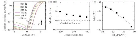
Fig.3.(a)Temperature-dependent forward J-V characteristics of SPND in semi-log scale with temperature varying from RT to 398 K.(b)Ideality factor as a function of temperature.(c)Richardson plot for Schottky barrier height extraction.

Fig.5.(a) Typical J-V characteristics of the GaN SPNDs with different Schottky metals in linear-scale and in semi-log scale.(b) The theoretically calculated built-in potential of SPNDs as a function of metals’work function and the turn-on voltage of fabricated SPNDs extracted at 1 A/cm2.
4.Conclusion and perspectives
With the adoption of a thin p-type layer between the Schottky metal and n-GaN layer, configuration of the SPND is realized in the vertical GaN rectifier with lowered turn-on voltage in comparison with the PND.Benefited from its typical single-carrier conduction characteristic,the GaN SPND is expected to fulfil the merits of high switching speed and low loss in power electronics applications.Additionally,the widerange variable turn-on voltage of SPND could facilitate the back-end circuit design and meet various diode specifications in different applications.
Acknowledgment
Project supported by the National Natural Science Foundation of China(Grant Nos.U2141241,62004099,61921005,and 91850112).
猜你喜歡
東方劍·消防救援(2024年2期)2024-03-18 09:03:38
美與時(shí)代·美術(shù)學(xué)刊(2022年3期)2022-04-27 01:35:55
瞭望東方周刊(2022年5期)2022-03-17 15:30:50
華人時(shí)刊(2021年17期)2021-11-12 20:09:49
音樂(lè)天地(音樂(lè)創(chuàng)作版)(2021年11期)2021-02-18 12:52:06
重慶與世界(2020年12期)2020-12-23 09:41:21
金沙江文藝(2019年7期)2019-07-29 01:57:06
藝術(shù)品(2018年5期)2018-06-29 02:14:58
水文地質(zhì)工程地質(zhì)(2017年3期)2017-06-21 15:10:27
金沙江文藝(2017年4期)2017-03-31 07:35:16

- Chinese Physics B的其它文章
- Analysis of cut vertex in the control of complex networks
- Atlas of dynamic spectra of fast radio burst FRB 20201124A
- Investigating the characteristic delay time in the leader-follower behavior in children single-file movement
- Micro-mechanism study of the effect of Cd-free buffer layers ZnXO(X =Mg/Sn)on the performance of flexible Cu2ZnSn(S,Se)4 solar cell
- Thermally enhanced photoluminescence and temperature sensing properties of Sc2W3O12:Eu3+phosphors
- Heterogeneous hydration patterns of G-quadruplex DNA