
Interface engineering of transition metal dichalcogenide/GaN heterostructures: Modified broadband for photoelectronic performance
2022-11-21 09:30:06YinluGao高寅露KaiCheng程開XueJiang蔣雪andJijunZhao趙紀(jì)軍
Chinese Physics B 2022年11期
Yinlu Gao(高寅露) Kai Cheng(程開) Xue Jiang(蔣雪) and Jijun Zhao(趙紀(jì)軍)
1Key Laboratory of Materials Modification by Laser,Ion and Electron Beams(Dalian University of Technology),Ministry of Education,Dalian 116024,China
2School of Electronic Engineering,Xi’an University of Posts and Telecommunications,Xi’an 710121,China
The GaN-based heterostructures are widely used in optoelectronic devices, but the complex surface reconstructions and lattice mismatch greatly limit the applications. The stacking of two-dimensional transition metal dichalcogenide(TMD= MoS2, MoSSe and MoSe2) monolayers on reconstructed GaN surface not only effectively overcomes the larger mismatch,but also brings about novel electronic and optical properties.By adopting the reconstructed GaN(0001)surface with adatoms(N-ter GaN and Ga-ter GaN),the influences of complicated surface conditions on the electronic properties of heterostructures have been investigated. The passivated N-ter and Ga-ter GaN surfaces push the mid-gap states to the valence bands,giving rise to small bandgaps in heterostructures. The charge transfer between Ga-ter GaN surface and TMD monolayers occurs much easier than that across the TMD/N-ter GaN interfaces,which induces stronger interfacial interaction and larger valence band offset(VBO).The band alignment can be switched between type-I and type-II by assembling different TMD monolayers, that is, MoS2/N-ter GaN and MoS2/Ga-ter GaN are type-II, and the others are type-I. The absorption of visible light is enhanced in all considered TMD/reconstructed GaN heterostructures. Additionally,MoSe2/Ga-ter GaN and MoSSe/N-ter GaN have larger conductor band offset(CBO)of 1.32 eV and 1.29 eV,respectively,extending the range from deep ultraviolet to infrared regime. Our results revel that the TMD/reconstructed GaN heterostructures may be used for high-performance broadband photoelectronic devices.
Keywords: GaN-based device, surface reconstructions, transition metal dichalcogenide (TMD), absorption spectra
1. Introduction
Group III nitrides are well-known wide-bandgap semiconductors with many applications in high-power, highvoltage and optoelectronic devices.The GaN-based blue lightemitting diodes (LED) realized the bright and energy-saving white light sources for the first time.[1]Moreover, the wide bandgap of GaN is suitable for deep ultraviolet (UV) optoelectronics. However, as the device application relies on the controlled heteroepitaxy of GaN thin film,which is essentially related to surface structure,deep knowledge about the atomic structure of GaN surface is highly desirable. Besides,a number of interfacial defects, mainly caused by the large lattice mismatch between GaN and the commonly used semiconductor materials(e.g.,Si and SiC),will heavily degrade the device performance.[2,3]During the same period, two-dimensional(2D)transition metal dichalcogenides(TMDs),such as MoX2(X= S, Se) with favorable mechanical properties, intrinsic direct bandgap of 1.1–1.9 eV and giant spin–orbit coupling(SOC), have attracted extensive attention in electronic and optoelectronic devices.[4,5]Most importantly, these 2D TMD monolayers and GaN have almost perfect lattice match of less than 1%.
With dangling bond free surface and weak van der Waals(vdW) interlayer interaction among intrinsic TMD materials,random combinations of TMD and GaN can be chosen to stack in arbitrary sequence to create heterostructures. Not limited to the properties of individual component, the heterostructures can combine superior properties of both TMDs and GaN to achieve diverse functions. Heterostructures of 2D TMD sheet and GaN substrate hold great technological promise. Benefited from the excellent absorption capability,WSe2/GaN interface was constructed to better utilize the visible light wavelength range for photocatalytic water splitting.[6]Under solar illumination, GaN and MoS2monolayers acted as electron donor and electron acceptor, respectively. Additionally,MoS2/GaN vdW heterostructure exhibited great optical absorption in ultraviolet and visible light wavelengths.[7]To protect the GaN surface from contamination, nitridized MoS2/GaN was used as photocatalyst for hydrogen generation by water splitting. Compared with the heterostructure without nitridation interfacial layer, the band edges of MoS2moved upward by about 0.5 eV,which led to better electron accumulation capability at the GaN side.[8]In addition to photocatalysis,gate-tunable heterostructure diodes through 2D/GaN junction concurrently exhibited over 7 orders of magnitude modulation in rectification ratios and conductance.[9]WS2/GaN p–n junction fabricated by vdW rheotaxy showed superior performance with a small leakage current density of 29.6 μA/cm2at-1 V.[10]MoS2/GaN and MoS2/AlGaN heterointerfaces were also promising for photodetection because of their high electron mobility. However, their optical absorbance was limited within the UV range, which restrained their deployment in broadband photodetectors.[11]
Despite the aforementioned advance,comprehensive understanding of the surface reconstruction at the interface of GaN-related heterostructures is still missing.In order to unveil the realistic surface condition of GaN, herein we address the most stable reconstructions of GaN (0001) surfaces, namely,N-ter GaN and Ga-ter GaN. The stability, electronic and optical properties of TMD/reconstructed GaN heterostructures have been investigated by using DFT calculations. The interaction between Ga-ter GaN surface and TMD monolayers are stronger due to the metallic character of Ga adatoms,resulting in larger valence band offset (VBO) than those of N-ter heterostructures. Both type-I and type-II band alignments can be attained by choosing TMD monolayer. In addition to the application in deep UV range, the larger CBO in MoSe2/Ga-ter GaN and MoSSe/N-ter GaN heterostructures provide opportunity for optoelectronic devices in short wavelength.
2. Computational methods
All calculations were implemented in Viennaab initiosimulation package (VASP) based on the density functional theory (DFT).[12]Within the generalized gradient approximation (GGA), PBE parameterization was selected for the exchange–correlation functional.[13]The electron–ion interactions were described by projector-augmented-wave potentials,and the electron wave functions were expanded in a plane wave basis with energy cutoff of 500 eV. For the Brillouin zone integration, a uniform spacing of 2π×0.03 ?A-1was used. The reconstructed GaN(0001)surface was modelled by a slab model with 4×4 lateral unit cells and five GaN bilayers.The underneath dangling bonds were saturated by pseudohydrogens with a valency of 0.75. Both GaN slab and TMD monolayers were relaxed until the force and energy was less than 0.01 eV/?A and 10-5eV,respectively,and the bottom layer of N atoms and pseudohydrogens were fixed. A 15 ?A vacuum layer was added to avoid the interaction due to periodic boundary condition. Our calculated lattice parameters for hexagonal GaN crystal and TMD(MoS2,MoSSe and MoSe2)monolayers are 3.24 ?A, 3.15 ?A, 3.22 ?A and 3.32 ?A, respectively, in good agreement with the experimental values(3.19 ?A,3.16 ?A,3.25 ?A,and 3.29 ?A).[14–16]
The bandgaps of GaN crystal and TMD monolayers are given in Table S1,which are underestimated with regard to the experimental values due to well-known deficiency of the PBE functional.[17]In contrast, electronic structure calculations with the Heyd–Scuseria–Ernzerhof (HSE06) functional[18]overestimate the bandgaps of these systems, and the deviations for TMD monolayers by HSE06 are even larger than PBE values. Hence, HSE06 calculation with 0.31 fraction of Fock exchange was only used to obtain an accurate bandgap of GaN crystal and surfaces. Benefited from the little lattice mismatch (<1%) between 4×4 TMD monolayer and GaN(0001) surface, the TMD/reconstructed GaN heterostructures can be constructed by directly stacking TMD monolayers and GaN slab together and fully relaxing the heterostructures. The lattice parameters of TMD monolayers were adjusted to that of GaN surface. The Grimme DFT-D3 method was adopted to account for the long-range vdW interactions between TMD layer and GaN surfaces.[19]
3. Results and discussion
We firstly address the structural stability and electronic properties of GaN (0001) surface and TMD monolayers separately. The symmetry and local structure of GaN surface have been subject of recent investigations. For the most relevant Ga-polar GaN (0001) surface, several reconstructions,including Ga-adatom, N-adatom and Ga vacancy structures have been proven to be stable.[20–22]Herein, we deal with the N-adatom and Ga-adatom reconstructed models,which are most energetically favorable under N-and Ga-rich condition,respectively. As shown in Figs. 1(a)–1(b), for the N-adatom model(N-ter GaN),an N atom is located at theH3hollow site,while in the case of Ga-adatom(Ga-ter GaN),the Ga adatom sits at theT4site right above the second-layer N atom. Moreover, the stability dependence on the location of adlayer for different models are employed theoretically (Fig. S1). The commonly considered N(H3)and Ga(T4)locations are found to be the most stable, which agree with the experimental observation by scanning tunneling microscopy (STM).[23]The average separation between the Ga (N) adlayer and the host Ga layer is about 1.71 ?A (1.12 ?A). To obtain more accurate electronic structures of GaN surfaces,HSE functional is used.After the passivation, only a small amount of mid-gap states exists in the valence bands, which means all the dangling bonds are filled by the surface free electrons(Figs.S2(a)and S2(b)). In addition to MoS2and MoSe2monolayers,we also consider a Janus system, i.e., MoSSe, which has been synthesized in laboratory.[24]From PBE calculations, monolayer MoS2,MoSSe and MoSe2sheets exhibit a bandgap of 1.83 eV,1.47 eV and 1.26 eV,respectively,and both valence band minimum (VBM) and conduction band maximum (CBM) come from Mo atoms.

Fig.1. Atom structures proposed for(a)N-adatom and(b)Ga-adatom GaN(0001)structures. The separation between the adlayer and host Gaterminated layer is 1.12 ?A and 1.71 ?A,respectively. (c)Structure of TMD(MoS2 or MoSe2)monolayer. (d)TMD/N-ter GaN heterostructure.

Table 1. Vertical inter layer distance (Δd), binding energies (Eb), bandgap(Eg) and the valence band offset (VBO) of TMD/reconstructed GaN heterostructures.
Taking MoS2/Ga-ter GaN as an example, six possible configurations of TMD/reconstructed GaN heterostructures with different atomic stacking orders are demonstrated in Fig.S3. As there are two sides in Janus MoSSe,two arrangements are possible for each heterostructure,which are referred to as MoSeS/GaN and MoSSe/GaN. According to the thermodynamic stability,all TMD/GaN heterostructures favor the C-type stacking configuration. For each heterostructure, the binding energy is calculated to characterize the TMD-GaN interaction as follows:

whereEhetero,EGaNandETMDrepresent the energy of the whole system, reconstructed GaN surface and TMD monolayer,respectively.The smaller binding energy means stronger attraction between MoS2and GaN surface. The vertical interlayer distance, binding energy and bandgap of all TMD/GaN heterostructures with C-type stacking are summarized in Table 1. The interlayer distance is in the range of 2–3 ?A. The interfacial interaction is also analyzed by using charge difference. In general,the charge depletion and accumulation cause electron wavefunction polarization,resulting in the formation of interface dipoles. In turn,the band alignment will be modified by the dipoles, which will be discussed later. As shown in Fig.2,charge transfer apparently takes place between GaN and TMD monolayer, where the charge depletion mainly occurs in the GaN side(cyan color), and TMDs sides are accumulation regions (yellow color). Bader charge donated from N-adatom GaN(Ga-adatom GaN)to MoS2and MoSe2are calculated to be about 0.3321e(0.7192e)and 0.1494e(0.3377e),respectively, suggesting stronger interaction for MoS2due to larger electronegativity of S than Se. Although the interlayer spacings between TMD layers and Ga-ter GaN surface are larger than those of N-ter GaN cases,Ga-ter GaN surface exhibits stronger interaction with TMD monolayers. Accordingly,the charge transfer across the interfaces is enhanced by the metallic nature of additional Ga atoms.
To shed further light on the underlying mechanism of orbital reconfiguration of TMD/GaN heterostructures, band structure and projected density of states (PDOSs) are calculated and presented in Fig. 3. For MoSe2/Ga-ter GaN heterostructure, both VBM and CBM are located at the highsymmetryΓpoint. While other TMD/GaN heterostructures are all indirect bandgap semiconductors. With PBE functional,the calculated bandgaps for MoS2/Ga-ter(N-ter)GaN,MoSeS/Ga-ter GaN, MoSSe/Ga-ter GaN and MoSe2/Ga-ter GaN are 0.38 eV (0.43 eV), 0.53 eV (0.46 eV), 0.59 eV(0.44 eV)and 0.44 eV(0.49 eV),respectively. Compared with those of GaN crystal(1.70 eV)and MoS2,MoSSe and MoSe2monolayers (1.83 eV, 1.47 eV and 1.26 eV), the bandgaps of TMD/GaN heterostructures are reduced due to the orbital reorganization. The mid-gap states come from the constructed GaN surface still exist, irrelevant to the stacking pattern of TMD monolayer. It is noteworthy that metallic states emerge at the interface when the interlayer distances are less than 2 ?A for the stacking configuration other than stack-C. Intuitively,for a given TMD/GaN heterostructure,the stacking configuration with semiconducting behavior should be more stable than those showing metallic behavior,as proven by our DFT calculations. In all TMD/N-ter GaN systems, strong hybridization occurs between 4d orbitals of Mo and N 2p orbitals,especially in MoSSe/N-ter GaN and MoSe2/N-ter GaN heterostructures.What is more, N 2p orbitals contribute mainly to the CBM,while the valance bands exhibit great orbital reorganization of TMD and N-ter GaN.The reorganization in TMD/Ga-ter GaN is much weaker than that in TMD/N-ter GaN heterostructures.

Fig.2.The differential electronic charge density for MoS2/N-ter GaN,MoSeS/N-ter GaN,MoSSe/N-ter GaN,MoSe2/N-ter GaN,MoS2/Ga-ter GaN,MoSeS/Ga-ter GaN,MoSSe/Ga-ter GaN and MoSe2/Ga-ter GaN heterostructures. The isosurface value is set be to 3×10⁻⁴ eV/Bohr3.Yellow and cyan colors represent the charge accumulation and depletion regions,respectively. The purple balls are N atoms,cyan balls are Ga atoms,yellow balls are S atoms,beige balls are Se atoms,green balls are Mo atoms and white balls are H atoms.
The band alignment at the interface of a heterostructure is of great importance for device applications. The charge transport behavior and optoelectronic response can be accurately controlled by forming different band alignments.In type-I heterostructure,both electrons and holes are restricted in the same domain with narrower bandgap,leading to quick electron–hole recombination. In consequence, type-I alignment is imperative for good performance in light emitting devices.In the case of type-II band alignment,either electrons or holes would migrate across the junction to reduce the system energy. Hence,electrons and holes could be well separated at different sides of a heterojunction, which is suited for optoelectronics and solar energy conversion. Herein, VBO against reconstructed GaN was calculated by using Wei’s core level method with the following equation:[25,26]

where the first term is the core level energy of Mo-3d with respect to the VBM of monolayer TMD,the second term represents the core level energy Ga-2p of GaN relative to its VBM,and the last term is the energy difference between the core level energy of Mo-3d and Ga-2p from TMD/GaN heterostructures. Since standard DFT methods are able to predict accurate ground-state energies, the PBE functional could be used to obtain the core level energy and offer a reference to align the VBM of the two systems. The band edges and VBO values of all considered heterostructures from PBE calculations are plotted in Fig.4. At the DFT-PBE level of theory,we have obtained VBOs of 1.40 eV and 1.80 eV for MoS2/N-ter GaN and MoS2/Ga-ter GaN, respectively, in good agreement with the reported theoretical and experimental values (1.32 eV–1.86 eV).[8,27,28]Both type-I and type-II band alignments have been formed by interface engineering of TMD layer and reconstructed GaN surface,that is,only MoS2/GaN heterostructure forms type-II alignment,while the others belong to type-I. Once the GaN surface is passivated with Ga adatoms, the energy band would bend more seriously, which lead to a larger VBO.Compared with N adatoms,the metallicity of Ga adatoms makes it easier for charge transfer to TMD materials, which are directly reflected by the Bader charge analysis and the differential charge density(Fig.2). The reconstructed model considered here can strongly affect the charge transfer across the interface, which directly determines the interfacial dipole. As a result, the VBO values for TMD/Ga-ter GaN are systematically larger than those of TMD/N-ter GaN by 0.6–0.3 eV. Due to the severely underestimated bandgaps from PBE,the experimental values are adopted(GaN:3.40 eV,MoS2:1.90 eV,MoSSe:1.68 eV and MoSe2:1.58 eV)to evaluate the CBO for TMD/reconstructed GaN heterostructure The calculated CBO values for MoS2/Ga-ter GaN (Nter GaN), MoSeS/Ga-ter GaN, MoSSe/Ga-ter GaN and MoSe2/Ga-ter GaN heterostructures are 0.30 eV (0.10 eV),0.28 eV(0.72 eV),0.68 eV(1.29 eV)and 1.03 eV(1.32 eV),respectively. From MoS2to MoSSe and finally to MoSe2,the CBO value gradually increases,which allow inter-subband energy spacing in the near-infrared range (CBO>1 eV).[29]These heterostructures are more desirable for considering the requirement of extended short wavelength devices. Compared with well-established three-dimensional AlGaN/GaN heterojunction for deep UV optoelectronic applications,[30,31]TMD/GaN heterostructures effectively extend the absorption range to short-wave infrared region by regulating the component chalcogen element in TMD.Currently, GaAs-based heterostructures are the commercially available extended short wavelength devices. The CBO values in MoSSe/N-ter GaN,MoSe2/Ga-ter GaN and MoSe2/N-ter GaN is comparable to and even larger than that in InGaAs/AlGaAs(~1 eV).[32]
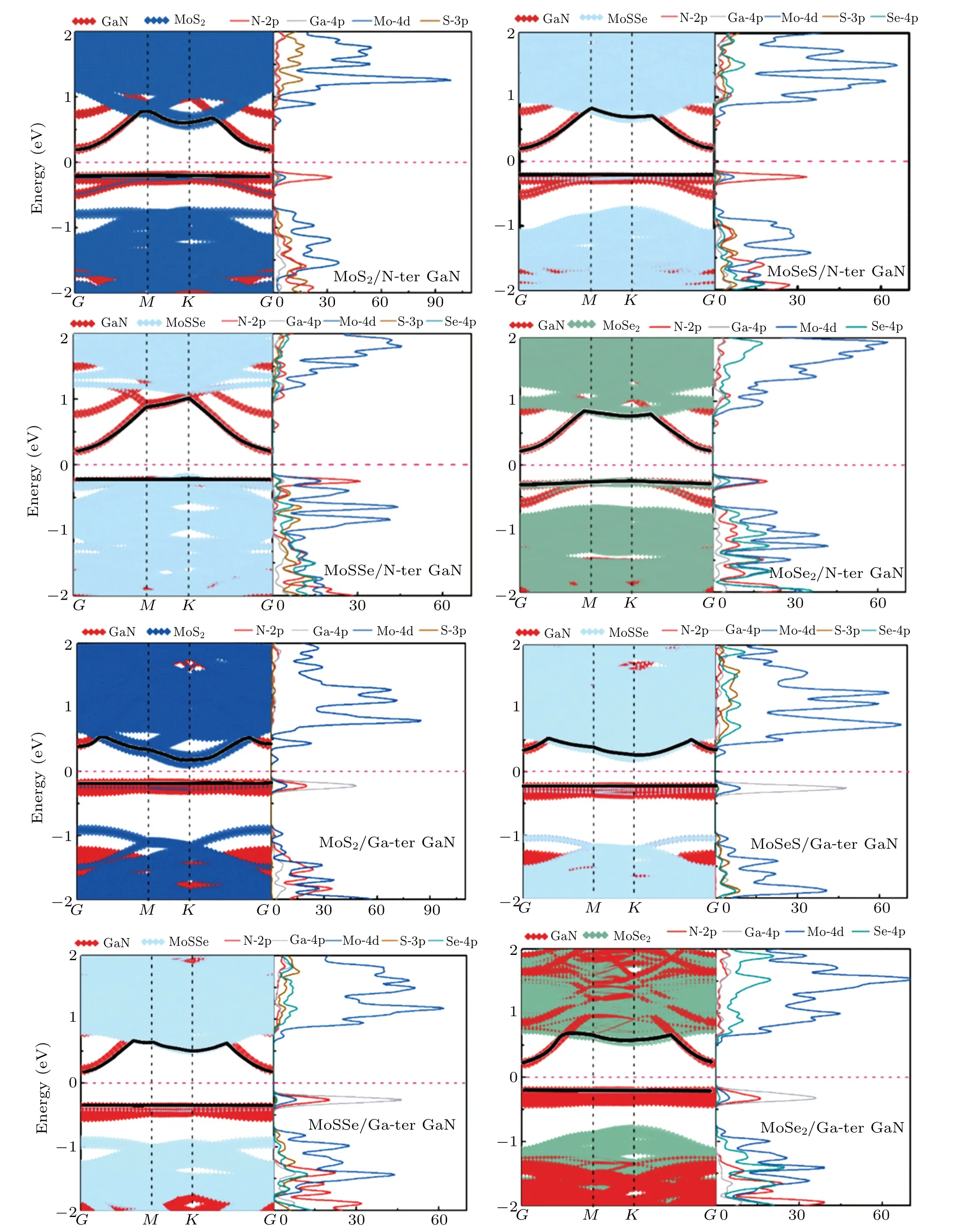
Fig.3. The electron band structure and projected density of states(PDOS)for(a)MoS2/N-ter GaN,(b)MoSeS/N-ter GaN,(c)MoSSe/N-ter GaN,(d)MoSe2/N-ter GaN,(e)MoS2/Ga-ter GaN,(f)MoSeS/Ga-ter GaN,(g)MoSSe/Ga-ter GaN and(h)MoSe2/Ga-ter GaN heterostructures.For each panel,the black dotted curves are the positions of VBM and CBM and the dashed line corresponds to the Fermi level.

Fig. 4. Band edge positions of (a) MoS2/N-ter GaN, (b) MoSeS/N-ter GaN, (c) MoSSe/N-ter GaN, (d) MoSe2/N-ter GaN, (e) MoS2/Ga-ter GaN,(f)MoSeS/Ga-ter GaN,(g)MoSSe/Ga-ter GaN and(h)MoSe2/Ga-ter GaN heterostructures with respect to the core levels. The bandgap of GaN crystal and monolayer MoS2,MoSSe and MoSe2 are adopted as the experimental values of 3.40 eV,1.90 eV,1.68 eV and 1.58 eV to determine the CBM positions. (i)The VBO values as function of TMD components.
Furthermore,the absorption spectra of TMD/reconstructed GaN heterostructures are simulated by computing the complex dielectric functionε(ω)=ε1(ω)+iε2(ω), where the imaginary partε2is related to the absorption at a given frequencyωand the real partε1is obtained fromε2by using the Kramers–Kronig relation. The absorption coefficient can be calculated by
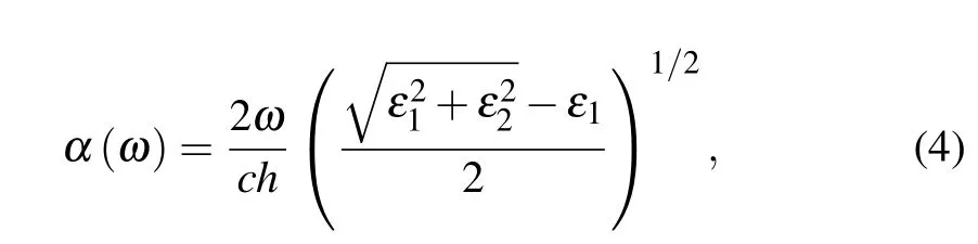
wherecrepresents the speed of light in vacuum.[33]Figure 5 depicts the optical absorption spectra of our TMD/reconstructed GaN heterostructures (up) and the individual GaN and TMD monolayers(bottom). Due to the wide bandgap, pristine GaN crystal hardly absorb the visible light.Both the additional atoms (Ga-ter and N-ter) and the interface engineering with TMD monolayers narrow the bandgap,which strongly enhance the absorption in visible regime. Nevertheless,the heterostructures with Ga-ter GaN surface absorb light more efficiently than N-ter structures. The threshold values for absorption of photon energy in MoSe2/Ga-ter GaN and MoSSe/N-ter GaN are near 0.9 eV, which correspond to the electronic transition from the VBM of MoSe2(MoSSe)to that of Ga-ter GaN(N-ter GaN).The pronounced absorption edges for the other heterostructures are between 1 eV and 1.2 eV.The optical absorption spectra confirm the possibility of short wavelength devices application, especially in MoSe2/Ga-ter GaN and MoSSe/N-ter GaN heterostructures,which coincide with the band alignment analysis.
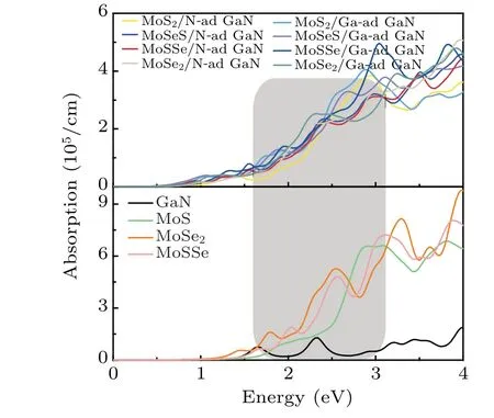
Fig. 5. Calculated optical absorption spectra for TMD/reconstructed GaN heterostructures(up)and the intrinsic GaN and TMD monolayers.The shaded area indicates the visible light range.
4. Conclusion
In summary,we have investigated the stability,electronic and optical properties of TMD/reconstructed GaN heterostructures based on DFT calculations. According to previous experimental evidences and our calculations,both the N-adatom and Ga-adatom reconstructed GaN(0001)surfaces are chosen as substrate of TMD monolayers(MoS2,MoSSe and MoSe2).The calculated binding energies reveal that, the larger electronegativity of S atoms induces stronger attraction between MoS2and GaN surface. The mid-gap states originated from the reconstructed GaN surface are retained after forming the heterostructures, which effectively narrow the bandgap. The interaction between Ga-ter GaN and TMD monolayers are stronger due to the metallic character of the additional Ga atoms, which also bring about larger VBO values than Nter heterostructures. Type-II band alignment is realized in MoS2/N-ter GaN and MoS2/Ga-ter GaN,while the others are type-I band alignment. Therefore, the band alignment can be switched between type-I and type-II by experimentally assembling different TMD monolayers. What is more, the capability of visible light absorption is enhanced in all heterostructures. Besides the application in the deep UV rage, the large CBO in selected TMD/reconstructed GaN heterostructures offer new opportunity for the extended short wavelength devices,especially in MoSe2/Ga-ter GaN and MoSSe/N-ter GaN heterostructures. The excellent broadband performances of TMD/reconstructed GaN heterostructures shed light on new photoelectronic devices using heterojunctions.
Acknowledgements
Project supported by the Science Challenge Project(Grant No. TZ2018004), the Natural Science Basic Research Program of Shaanxi Province, China (Grant No. 2021JQ-697), the National Natural Science Foundation of China (Grant Nos. 11874097, 91961204, and 12004303), XinLiaoYingCai Project of Liaoning Province,China (Grant No. XLYC1905014), and Key Research and Development Project of Liaoning Province, China (Grant No. 2020JH2/10500003). We thank Supercomputing Center of Dalian University of Technology.

- Chinese Physics B的其它文章
- Microwave absorption properties regulation and bandwidth formula of oriented Y2Fe17N3-δ@SiO2/PU composite synthesized by reduction–diffusion method
- Amplitude modulation excitation for cancellous bone evaluation using a portable ultrasonic backscatter instrumentation
- Laser-modified luminescence for optical data storage
- Electron delocalization enhances the thermoelectric performance of misfit layer compound(Sn1-xBixS)1.2(TiS2)2
- TiO2/SnO2 electron transport double layers with ultrathin SnO2 for efficient planar perovskite solar cells
- Sputtered SnO2 as an interlayer for efficient semitransparent perovskite solar cells