
Fluorine-plasma treated AlGaN/GaN high electronic mobility transistors under off-state overdrive stress
2022-11-21 09:38:08DongyanZhao趙東艷YuboWang王于波YanningChen陳燕寧JinShao邵瑾ZhenFu付振FangLiu劉芳YanrongCao曹艷榮FaqiangZhao趙法強(qiáng)MingchenZhong鐘明琛YasongZhang張亞松MaodanMa馬毛旦HanghangLv呂航航ZhihengWang王志恒LingLv呂玲XuefengZheng鄭雪峰andXiaohuaMa馬曉華
Chinese Physics B 2022年11期
Dongyan Zhao(趙東艷) Yubo Wang(王于波) Yanning Chen(陳燕寧) Jin Shao(邵瑾) Zhen Fu(付振)Fang Liu(劉芳) Yanrong Cao(曹艷榮) Faqiang Zhao(趙法強(qiáng)) Mingchen Zhong(鐘明琛)Yasong Zhang(張亞松) Maodan Ma(馬毛旦) Hanghang Lv(呂航航) Zhiheng Wang(王志恒)Ling Lv(呂玲) Xuefeng Zheng(鄭雪峰) and Xiaohua Ma(馬曉華)
1Beijing Engineering Research Center of High-reliability IC with Power Industrial Grade,Beijing Smart-Chip Microelectronics Technology Co.,Ltd.,Beijing 100192,China
2Beijing Chip Identification Technology Co.,Ltd.,Beijing 102200,China
3School of Electro-Mechanical Engineering,Xidian University,Xi’an 710071,China
4Key Lab of Wide Band-Gap Semiconductor Materials and Devices,Xidian University,Xi’an 710071,China
Influences of off-state overdrive stress on the fluorine-plasma treated AlGaN/GaN high-electronic mobility transistors(HEMTs) are experimentally investigated. It is observed that the reverse leakage current between the gate and source decreases after the off-state stress,whereas the current between the gate and drain increases. By analyzing those changes of the reverse currents based on the Frenkel–Poole model,we realize that the ionization of fluorine ions occurs during the off-state stress. Furthermore,threshold voltage degradation is also observed after the off-state stress,but the degradations of AlGaN/GaN HEMTs treated with different F-plasma RF powers are different. By comparing the differences between those devices,we find that the F-ions incorporated in the GaN buffer layer play an important role in averting degradation.Lastly,suggestions to obtain a more stable fluorine-plasma treated AlGaN/GaN HEMT are put forwarded.
Keywords: AlGaN/GaN HEMT,fluorine plasma treatment,off-state overdrive stress
1. Introduction
GaN and related alloys have shown greater promise in high-temperature, high-power and high-frequency applications compared to traditional semiconductor materials.[1–3]Owing to such excellent performance characteristics as high saturation current,high cutoff frequency,and large power handling capabilities,AlGaN/GaN high-electron mobility transistors (HEMTs) are promising candidates for next-generation microwave power amplifiers and high-voltage switches.[4–8]The conventional AlGaN/GaN HEMTs are the depletionmode (D-mode) devices with a negative threshold voltage(Vth). In practice, the enhancement-mode (E-mode) HEMTs provide a simplified solution for circuit designing and can combine with D-mode HEMTs to realize the integrated D/Emode digital circuits. Fluorine-plasma (F-plasma) treatment is an effective approach to converting AlGaN/GaN HEMTs from D-mode to E-mode.[9,10]Because of the high electronegativity, the F atoms, which are incorporated in the AlGaN barrier layer and the GaN buffer layer, tend to capture free electrons and become negative fixed charges which will help to deplete the two-dimensional electron gas(2DEGs)and deliver a positive shift ofVth.[11,12]The change ofVthis roughly linear with the power and treatment time of CF4plasma,[13]which means that the conditions of F-plasma treatment have a strong effect on the threshold voltage (Vth) of the device.Therefore, F-plasma treated AlGaN/GaN HEMTs have great application prospects. However, when the F-plasma treated HEMT is biased under stress conditions,those F-ions are unstable,and they may diffuse or be ionized during thermal stress and overdrive stress,[14–17]resulting in degradation of device performance.Some works proposed that the high-energy electrons injected under the gate will collide with F-ions during the stress,causing the threshold voltage to move negatively.[18,19]Some works put forward that degradation of GaN HEMTs treated by F-plasma RF power is related to migration of F-ions under the overdrive stress,and the dynamic equilibrium of Fions migration movement causes the degradation to be saturated gradually.[20]However,there are also some other works claimed that the degradation may be caused by the growing defects in the barrier layer during high field stress.[17,21]From the above discussion, though extensive research on F-plasma treated AlGaN/GaN HEMTs has been carried out over the last decade,the degradation mechanism under overdrive stress remains unclear. Therefore, it is essential to improve the physical understanding of the degradation mechanisms,and to put forward effective solutions to prevent those degradations or to fabricate more stable F-plasma treated devices for real applications.
In this paper,F-plasma treated AlGaN/GaN HEMTs dealt with different F-plasma RF powers are stressed under the offstate overdrive conditions. A study on the performance and parameter variation between the fresh devices and the stressed devices is carried out in detail. The impacts of different Fplasma RF powers on the parameter degradation of stressed F-plasma treated devices are investigated. Suggestions to obtain a more stable F-plasma treated AlGaN/GaN HEMT are put forwarded lastly,and we present a novel device which can reduce the degradation caused by the instability of F-ions.
2. Devices and experiments
Figure 1 shows the schematic diagram of the F-plasma treated HEMTs used in this study. The AlGaN/GaN heterostructure,which was grown on a(0001)sapphire substrate by metal-organic chemical vapor deposition(MOCVD),consists of a GaN nucleation layer, a 2-μm-thick unintentionally doped GaN buffer layer,and an unintentionally doped 20-nmthick Al0.3Ga0.7N barrier layer. Room-temperature Hall measurements show that the concentration and the electron mobility of the 2DEGs are 1.12×1013cm-2and 1615 cm2/(V·s),respectively. Ohmic contacts were based on a Ti/Al/Ni/Au(22 nm/140 nm/55 nm/45 nm) metallic system, which were followed by thermal annealing in nitrogen at 830°C for 30 s,yielding a contact resistance typically around 1.0 Ω·mm. The Ni/Au/Ni (45 nm/200 nm/20 nm) Schottky gate was realized by the electron-beam evaporation technology. The gate length and width of devices are 0.5 μm and 100 μm,respectively.
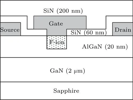
Fig.1. Cross section of those F-plasma treatment HEMTs.
During the fabrication process of the F-plasma treated AlGaN/GaN HEMTs, before depositing the Schottky contact metal of the gate, the reactive ion etching (RIE) technology is utilized to perform the F-plasma treated process while CF4is used as the F source. The window at the Schottky contact area is the opening region while the other region is protected by the photoresist. Therefore, the F-ions can be implanted into the specific region. The power and time of RIE treatment determine the depth and amount of F-ions implanted.Obviously, the characteristics of the devices obtained under different conditions of F-plasma treatment are different. For comparison,HEMTs treated with different F-plasma RF powers are required. Three kinds of HEMTs, i.e., samples A, B and C,were fabricated with the same structure,except that the Schottky contact areas of different samples were treated with CF4plasma under different conditions. Table 1 shows the Fplasma treatment conditions of the three kinds of HEMTs. In addition, the F-plasma treated AlGaN/GaN Schottky barrier diodes were also fabricated using the same technology.

Table 1. Samples obtained under different conditions of F-plasma treatment.

3. Results and discussion
3.1. Experiments details
The initial DC transfer and transconductance characteristics of all samples are presented in Fig. 2(a), and it is observed that all samples can work normally. In addition,theVthof samples A (without F-plasma treatment), B (the F-plasma RF power and time are 80 W, 120 s) and C (the F-plasma RF power and time are 130 W,120 s)are-2.81 V,-0.26 V,and 0.42 V,respectively,matching with the previous research which indicates that the threshold voltage of the F-plasma treated AlGaN/GaN HEMTs increases with the F-plasma RF power.[22]It is noteworthy that theVthof sample C is positive,which indicates that sample C has been delivered to the Emode. Figure 2(b)presents the output characteristic of sample C(E-mode HEMT).

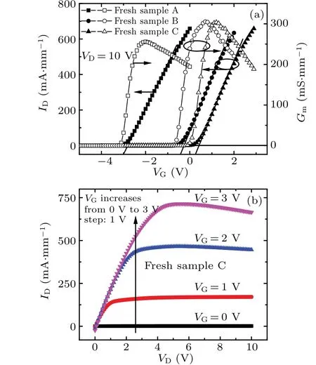
Fig.2. (a)DC transfer and transconductance characteristics of fresh samples A,B,C.(b)Output characteristic of fresh sample C(E-mode HEMT).

Fig.3. The schematic of the device under the off-state stress.
3.2. The reverse currents of SBD1 and SBD2
The reverseI–Vcharacteristics of SBD1 andSBD2 before and after the stress are shown in Figs. 4(a) and 4(b), respectively. It is obvious that the reverse leakage currents of SBD1 in samples B and C both decrease after the off-state stress, while the reverse leakage currents of SBD2 both increase. For the F-plasma treated SBDs, the transport mechanism of the reverse leakage current is supposed to be the Frenkel–Poole emission from the F-related deep level states into the dislocations related continuum states,[23]and the Frenkel–Poole emission current density is given by[24]
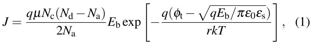
whereJis the emission current density,qis the charge of an electron,μis the carrier mobility,Ncis the effective density of states in the conduction band,Ndis the density of donor sites,Nais the density of acceptor sites,φtis the barrier height for electron emission from a trap state,Ebis the electric field in the AlGaN barrier layer,εsis the high-frequency relative dielectric permittivity,εis the permittivity of vacuum,Tis thermodynamic temperature,kis Boltzmann’s constant,andris a parameter ranging from 1 to 2 depending on the position of the Fermi level. In the case ofn ?Na,n ?Nd(nis the number of electrons in the conduction band),r=1;in the case ofNa?n,Na?Nd,r=2.

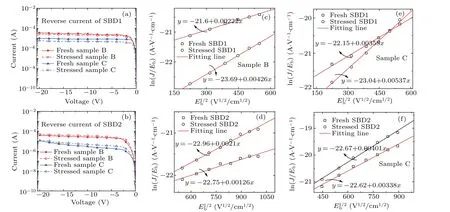
Fig.4. The reverse I–V characteristics of(a)SBD1 and(b)SBD2 before and after stress. The plots of ln(J/Eb)versus E1/2b for both(c)SBD1 and(d)SBD2 of sample B before and after stress. The plots of ln(J/Eb)versus E1/2b for both(e)SBD1 and(f)SBD2 of sample C before and after stress.
3.3. The ionization of F-ions effect on SBD1
With devices biased under the reverse voltage stress, a high electric field is formed. Many gate electrons are injected into the AlGaN barrier and are accelerated by this electric field. When exposed to the negatively charged F-ions, those electrons, which have got huge kinetic energy, can ionize the F-ions.[26]The stable Ga–F bonds are formed during the process of the ionization of F-ions.[15]With the Ga-F bonds occupied some gallium atoms, some nitrogen atoms cannot form enough bonds with the gallium atoms to become saturated,causing the increase of the unsaturated nitrogen. The unsaturated nitrogen atoms are mainly acting as acceptors of electrons in the crystal, indicating that theNaincreases after the stress. As theNaincreases, the relationship amongn,NaandNdgets closer to the case ofn ?Na,n ?Nd,which indicates that the value ofrgets closer to 1, meaning that the value ofrdecreases after the stress. According to Eqs. (3) and (4),changes ofNaandrresult in the decrease of the intercept(B)and the increase of the slope(A),which agree with the above experimental data of SBD1 shown in Figs.4(c)and 4(e).
Furthermore, because of the high electric field, many traps are generated at the gate-metal/AlGaN interface. Those new traps can capture electrons after the stress and lead to Fermi-level pinning with a lower level at the Gate metal/AlGaN interface,[27]which will increase the barrier heightφtof FP emission and result in the reduction of the reverse leakage current in SBD1(as shown in Fig.4(a)).In addition, the ionization of the negatively charged F-ions weakens the depletion effect on 2DEGs,leading to the negative shift of the threshold voltage. In order to verify the above analysis,the fluorine plasma treated AlGaN/GaN SBDs are stressed under the condition ofVGSTRESS=-10 V for 1000 s. Figure 5 shows theC–Vcharacteristics of those devices. It is seen that the threshold voltage decreases with the increasing stress time,consistent with the above analysis. Thus, some F-ions in the SBD1 were ionized during the off-state stress.
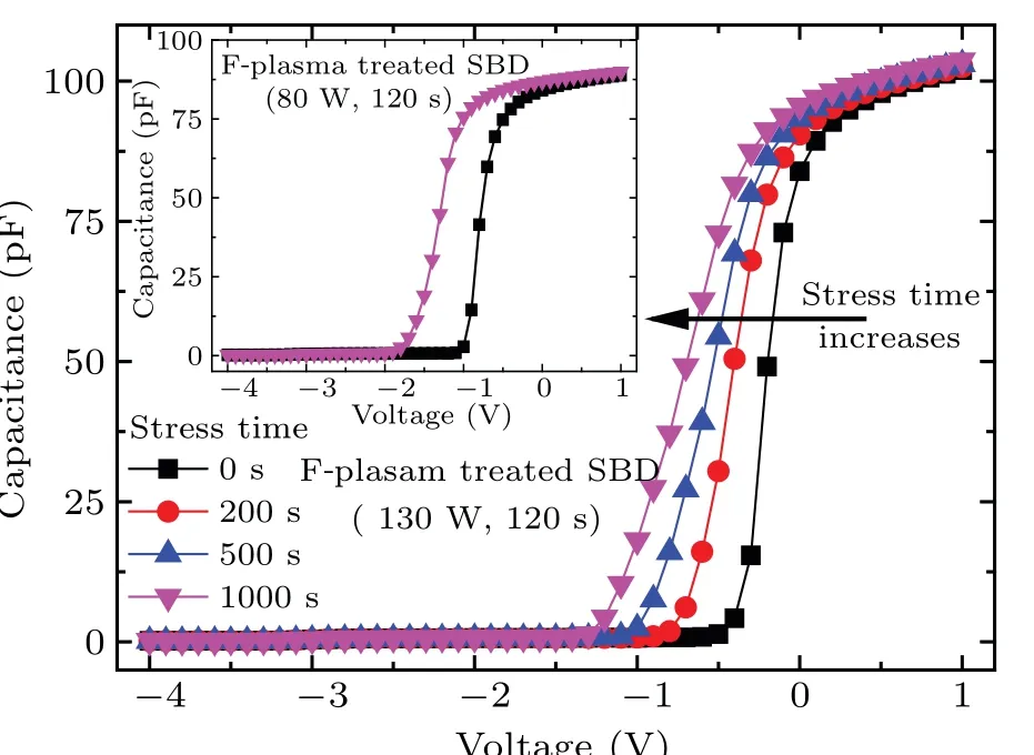
Fig.5. The C–V characteristics of fluorine plasma treated AlGaN/GaN SBDs under the stress condition of VG STRESS = -10 V at different stress times. The F-plasma treated AlGaN/GaN SBD is circular, and the diameter of its anode is 130 μm; the distance between anode and cathode is 30 μm.
From the above analysis of SBD1, it can be concluded that some F-ions in the devices can be ionized during the high stress,which results in the decreased intercept(B)and the increased slope (A) of the SBD1 at last. Furthermore, theC–Vcharacteristics can prove the analysis.
3.4. Synergistic effects of F-ions ionization and inverse piezoelectric effect on SBD2
The stress condition ofVGSTRESS=-25 V for SBD2 is larger than the critical voltage (VC), over which an Al-GaN/GaN HEMT will experience the inverse piezoelectric effect (the typical value ofVCis about-20 V[28]). Thus,the inverse piezoelectric effect induced lattice defects may be formed in the AlGaN barrier layer after the stress. Those lattice defects are as donors of electrons in the crystal,[29]indicating the increase of theNdand the consequent increase of then. AsnandNdboth increase,the relationship amongn,NaandNdgets more close to the case ofNa?n,Na?Nd,which indicates that the value ofrgets more close to 2,meaning that the value ofrincreases after the stress. According to Eqs.(3)and(4),the increases of therandNdresult in the decrease of slope(A)and the increase of intercept(B),respectively. However,the transport mechanism of the leakage current in SBD2 is still the Frenkel–Poole emission, and the ionization of the F-ions also occurs during the stress, which still results in the increase of slope(A)and the decrease of intercept(B),respectively. Those two effects will counteract each other,as shown in Figs.4(d)and 4(f). At last,the increase of the slope(A)and the decrease of intercept (B) become weak in SBD2 by the synergistic effects of ionization of F-ions and inverse piezoelectric effect.
In addition, those lattice defects may increase the trapassisted-tunneling(TAT)current. Also,they may overlap with each other and form a leakage path, resulting in the increase of the reverse leakage current(as shown in Fig.4(b)). Moreover, the lattice defects, produced by the inverse piezoelectric effect can increase the scattering of conduction electrons,which will result in the increase of the channel resistance. In order to proof the inverse piezoelectric effect,the channel resistancesRonof sample B before and after the off-state stress are extracted from the output characteristic and are presented in Fig. 6. It shows thatRonincreases after the stress, which results from the formation of the lattice defects at the Al-GaN/GaN interface and agrees with the above analysis.
From the above analysis of SBD2,we can obtain that Fions ionization and the inverse piezoelectric effect can both occur near the drain under the high off-state stress, and the synergistic effect weakens the increase of the slope (A) and the decrease of intercept(B)in SBD2. The increasedRonapproves the conclusion.
3.5. Effect of F-ions on Vth
According to the above analyses, the ionization of the negatively charged F-ions arises around the both ends of the gate (SBD1 and SBD2) during the overdrive stress, which weakens the depletion effect of F-ions on 2DEGs, leading to the increase of the 2DEG density and the consequent negative shift of threshold voltage. However, as shown in Fig. 7,Vth’s of samples B and C have different degradations under the same stress condition. In detail,Vthof sample B degrades under the off-state stress and the degradation becomes serious as the stress time increases,whileVthof sample C degrades much smaller. There are three reasons for this phenomenon.

Fig.7. Stress time dependence of Vth of samples A(square),B(circle)and C(triangle)under the off-state stress.
(i)The amount of injected electrons from the gate.
During the off-state stress,the ionization of the F-ions in AlGaN is caused by the injected gate electrons,and the quantity of the ionized F-ions is related to the amount of injected electrons. Therefore, the degradation ofVthshows strong dependence on the injected electron density.[16,26]According to Figs.4(a)and 4(b),the reverse leakage currents of both SBD1 and SBD2 in sample C are much smaller than those in sample B,which means that the injected electrons from the gate in sample C are much less than those in sample B.Consequently,the quantity of the ionized F-ions in sample C is much smaller than that in sample B,and theVthdegradation of sample C is not pronounced.
(ii)The depth of F-ions in the AlGaN barrier layer.
The depth of F-ions implantation in the AlGaN barrier layer increases with the increase of the F-plasma RF power.The ionization of the F-ions arises in the AlGaN barrier layer around the both ends of the gate(SBD1 and SBD2). If the offstate stress time is long enough,as shown in Fig.8,the F-ions,which exist in the two triangle regions (SBD1 and SBD2),will be ionized after the stress, while the others will maintain mostly. The deeper the F-ions stay in the AlGaN layer,the more the F-ions will maintain after the off-state stress.Thus, the maintained F-ions in sample C treated with higher F-plasma RF power(130 W)are more than those in sample B treated with lower F-plasma RF power(80 W),which leads to the largerVthdegradation in sample B while smallerVthdegradation in sample C.

Fig. 8. The schematic of the F-ions distribution in fresh and stressed samples B(80 W)and C(130 W).
(iii)F-ions located at the GaN buffer layer.
The F-ions,which stay in the top layer of the GaN buffer layer,also play an important role in the depletion effect of the 2DEG.They can deplete the 2DEG and deliver a positive shift ofVth, too. TCAD simulation is employed and the structure parameters are the same for the devices used in the experiments, such as a 2-μm-thick GaN buffer layer, an unintentionally doped 20-nm-thick Al0.3Ga0.7N barrier layer,0.5 μm gate length and 100 μm gate width. Under the off-state overdrive stress condition(VG=-10 V,VD=15 V,VS=0 V),the gate region electric field in the AlGaN barrier layer is stronger than that in the GaN buffer layer as shown in Fig. 9, which means that F-ions in the GaN buffer layer can avoid being influenced by the overdrive stress. For sample C, as shown in Fig. 8, because of the larger plasma treatment power, more F-ions stay in the GaN buffer layer and more F-ions retain after the off-state overdrive stress. Thus, the overdrive stress has a smaller influence on theVthof sample C. Our previous work also shows that, during the reverse gate step-stress, theVthof thin barrier F-plasma treated HEMTs are much more stable than that of the devices with a thicker barrier layer(those two kinds of devices are treated with the same CF4plasma RF power),[30]which may be caused by the F-ions which are incorporated in the GaN buffer layer.
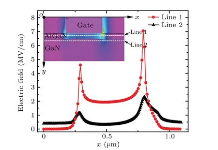
Fig. 9. Extracted electric field intensity distribution of lines 1 and 2 in AlGaN/GaN HEMT under off-state stressing condition, lines 1 and 2 are located respectively in the AlGaN barrier layer and in the GaN buffer layer. Inset: contour plot of electric field round the gate. The simulation is carried out with the TCAD simulator Silvaco Atlas, and the VD is set at 15 V,VG is set at-10 V and VS is set at 0 V.
3.6. Methods to improve the stability of F-plasma treated devices
Combining with the above analyses and explanations,we can realize that the unreliable performance of F-plasma treated AlGaN/GaN HEMTs under off-state overdrive stress is mainly caused by the ionization of the negatively charged F-ions. The degree ofVthdegradation is related to the quantity of the ionized F-ions. For sample C, most of the negatively charged F-ions are retained,resulting in the negligibleVthdegradation.
Furthermore, as the ionization of the negatively charged F-ions is caused by the high electric field in the gate region,there are two ways to improve the stability and reliability of Fplasma treated devices: optimizing the distribution of electric field and changing the location of implanted F-ions. The gatefield-plate and dual-gate structure can be used to optimize the distribution of electric field around the gate region of F-plasma treated HEMTs.[14]Noticeably, before applications, it is necessary to do much work such as simulation of those structures and exploration of the optimal structural parameters, which will take a long time.Since the electric field of overdrive stress in the GaN buffer layer is weak and it has little influence on the F-ions incorporated in the GaN buffer layer, more stable F-plasma treated devices can be obtained when we focus on only implanting F-ions into the GaN buffer layer.One of these ideal stable F-plasma treated AlGaN/GaN HEMTs is shown in Fig.10. TACD simulation shows that a smaller number of F-ions can convert the D-mode HEMTs into E-mode in this novel structure than that in the normal structure. The research on the manufacturing process for this structure is ongoing.

Fig.10. An ideal stable F-plasma treated HEMT.F-ions only incorporated in the GaN buffer layer.
4. Conclusions
In summary, we have investigated the influences of the off-state overdrive stress on the F-plasma treated AlGaN/GaN HEMTs. After the off-state stress, the reverse leakage current between gate and source, as well as that between gate and drain, changes. The Frenkel–Poole model is carried out to analyze those changes of the reverse current and it suggests that the variation of the gate-source leakage current is mainly caused by the ionization of the F-ions, and that of the gatedrain leakage current is caused by the synergistic effects of the ionization of F-ions and inverse piezoelectric effect. TheC–Vcharacteristics and extracted channel resistances both bring a good agreement on those analyses. Furthermore, the reasons for differentVthdegradations of HEMTs treated by different powers of F-plasma are discussed too. It is indicated that the F-ions incorporated in the GaN buffer layer can play an important role in averting degradation. Lastly,suggestions to obtain a more stable fluorine-plasma treated AlGaN/GaN HEMT are put forward,and a novel structure is also suggested.
Acknowledgements
Project supported by the Laboratory Open Fund of Beijing Smart-Chip Microelectronics Technology Co., Ltd and the National Natural Science Foundation of China (Grant Nos. 11690042 and 12035019), the National Major Scientific Research Instrument Projects(Grant No.61727804),and the Natural Science Foundation of Shaanxi Province, China(Grant No.2022-JM-386).

- Chinese Physics B的其它文章
- Microwave absorption properties regulation and bandwidth formula of oriented Y2Fe17N3-δ@SiO2/PU composite synthesized by reduction–diffusion method
- Amplitude modulation excitation for cancellous bone evaluation using a portable ultrasonic backscatter instrumentation
- Laser-modified luminescence for optical data storage
- Electron delocalization enhances the thermoelectric performance of misfit layer compound(Sn1-xBixS)1.2(TiS2)2
- TiO2/SnO2 electron transport double layers with ultrathin SnO2 for efficient planar perovskite solar cells
- Sputtered SnO2 as an interlayer for efficient semitransparent perovskite solar cells