
Surface properties of Al-doped ZnO thin film before and after CF4/Ar plasma etching
2022-08-01 11:35:10YoungHeeJOOGwanHaKIMDooSeungUMandChangIlKIM
Plasma Science and Technology 2022年7期
Young-Hee JOO,Gwan-Ha KIM,Doo-Seung UMand Chang-Il KIM,?
1 School of Electrical and Electronics Engineering,Chung-Ang University,Seoul 06974,Republic of Korea
2 Department of Semiconductor Materials and Applications,Korea Polytechnic,Seongnam 13122,Republic of Korea
3 Department of Electrical Engineering,Sejong University,Seoul 05006,Republic of Korea
Abstract Al-doped ZnO(AZO)is considered as an alternative to transparent conductive oxide materials.Patterning and achieving a stable surface are important challenges in the development and optimization of dry etching processes,which must be overcome for the application of AZO in various devices.Therefore,in this study,the etch rate and surface properties of an AZO thin film after plasma etching using the adaptive coupled plasma system were investigated.The fastest etch rate was achieved with a CF4/Ar ratio of 50:50 sccm.Regardless of the ratio of CF4 to Ar,the transmittance of the film in the visible region exceeded 80%.X-ray photoelectron spectroscopy analysis of the AZO thin film confirmed that metal-F bonding persists on the surface after plasma etching.It was also shown that F eliminates O vacancies.Consequently,the work function and bandgap energy increased as the ratio of CF4 increased.This study not only provides information on the effect of plasma on AZO thin film,but identifies the cause of changes in the device characteristics during device fabrication.
Keywords:Al-doped ZnO,plasma etching,F-based plasma,surface characteristics,X-ray photoelectron spectroscopy,ultraviolet photoelectron spectroscopy
1.Introduction
Wide bandgap,n-type zinc oxide(ZnO)with a wurtzite crystal structure is utilized in a range of applications such as optical devices,sensors and solar cells[1–4].ZnO is also a very interesting material due to its advantages such as low cost and high physical and chemical stability[5,6].ZnO is also attracting attention as a suitable host material for doping with other metals[7].Therefore,research into improving the electrical and optical properties by doping ZnO thin films with many metal elements(Al,Ga,B,In,etc)is in progress[8–10].Al-doped ZnO(AZO),which has high transmittance and very low resistivity(<8.5×10⁻⁵Ω·cm),has attracted attention as an alternative to indium tin oxide(ITO)films[11,12].AZO thin films containing very low proportions of Al are advantageous because the main component is low-cost,non-toxic ZnO-based thin films.AZO is the best candidate as a transparent conductive oxide(TCO)material from the perspective of cost,availability and environmental friendliness[12,13].Therefore,AZO is considered as an alternative to TCO for solar cells,light-emitting diodes(LEDs)[14],photodetectors[15]and touch panels[16].
From a manufacturing point of view,TCO films with AZO can be easily etched to form microelectrodes for optoelectronic and display devices.The level of reduction of the pattern size that can be achieved with wet etching is limited due to the isotropic nature of this process,and it is difficult to achieve fine control of the process.In contrast,dry etching is advantageous for obtaining micro/nanoscale patterning due to its anisotropic characteristics and the ability to achieve fine process control.Therefore,the development and optimization of dry etching processes for AZO thin films are important challenges that must be overcome to enable accurate patterning and achieve stable device parameters.Dry etching of AZO has been studied by several groups[17,18].The etching properties and mechanism of etching AZO thin films in Cl-based plasma have been studied,demonstrating that Cl radicals play a dominant role in the etching process[19].In the Cl-based plasma(such as Cl2or BCl3)etching process,etching generally involves Zn–Cl bonds or compounds containing B[17,20].In contrast,the etching properties and etching mechanism of AZO thin films using F-based plasma have received little attention[18,21].Most studies focused on improving the device performance rather than the etching mechanism of AZO thin films.Thus,a detailed description of the etching characteristics is required.
In this study,the etching characteristics of AZO thin film and changes in the surface properties(e.g.work function,band gap,surface roughness,etc)of the thin film before and after etching were investigated according to the CF4/Ar plasma concentration.The plasma etching process is performed with adaptive coupled plasma(ACP)equipment.After the etching process,the surface roughness was confirmed using atomic force microscopy(AFM)and field emission scanning electron microscopy(FE-SEM),and changes in the chemical composition and work function of the AZO thin film were observed using X-ray photoelectron spectroscopy(XPS)and ultraviolet photoelectron spectroscopy(UPS).In addition,the transmittance and band gap changes of the AZO thin film were confirmed using UV–vis spectrophotometry.
2.Experiment
AZO thin films were deposited on n-type Si(100)and glass substrates(Marienfeld,Germany)by radio frequency(RF)magnetron sputtering.Before deposition,the Si and glass substrates were sequentially ultrasonically cleaned with isopropyl alcohol(IPA),and DI water,and finally dried with nitrogen gas.AZO thin films were deposited using a ZnO/Al2O3(98/2 wt.%)target.The AZO target,2 inches in diameter and 1/8 inch thick,was bonded to copper-backed plates.The target and substrate were placed parallel to each other at a distance of 10 cm.After maintaining the initial vacuum of the chamber at 5.5×10⁻⁵Torr for 3 h using a rotary pump and diffusion pump,Ar gas was injected using a mass flow controller.The RF magnetron sputtering system applied a power of 13.56 MHz to the electrodes,and the power input was controlled using a matching network system and RF generator.Before deposition of the AZO thin films,chamber stabilization and target cleaning were achieved by 10 min pre-sputtering with Ar plasma.After that,the AZO thin film was deposited on the substrate with an RF power of 60 W,Ar flow of 30 sccm,working pressure of 5×10⁻³Torr,deposition temperature of 300°C and deposition time of 60 min.Based on our previous experiments,AZO thin films exhibited the highest transparency and electrical conductivity properties under the above conditions[22].
The plasma etching process was performed using an ACP system.The ACP source consisted of a plate-shaped electrode in the center of the process chamber,which was spirally surrounded by a coil electrode[23].The ACP source above the main process chamber was connected to a 13.56 MHz RF power supply.Another 2 MHz RF power supply was connected separately to the substrate to induce a bias power across the substrate.The main process chamber maintained the initial vacuum using rotary and turbo molecular pumps.By attaching a load-lock chamber to the ACP system,the system introduced the wafer into the process chamber while maintaining the process chamber under a high vacuum.An optical emission spectroscopy(OES)system was connected to the viewport of the main process chamber.The cooling system cooled the substrate.Since the etching parameters,such as the etch rate and surface roughness,are closely related to the temperature of the substrate surface,it is important to keep the substrate temperature constant[24].The wafer substrate cooled by the chiller was maintained at 21 °C.
The effect of the CF4/Ar ratio on the basic etching properties was investigated while maintaining the total flow rate of the gas at 100 sccm.Various etch parameters(RF power,bias power to the substrate,and process pressure)were used to evaluate the etching properties and etching mechanism of the AZO thin film.The etch rate as a function of etch parameters was investigated using a surface profiler(α-step 500,KLA Tencor).In addition,the surface roughness change and morphology of the AZO thin film were confirmed using AFM(NX-10,Park system)in tapping mode and an FE-SEM(Sigma 300,Carl Zeiss).For accurate FE-SEM measurements,a platinum coating was applied to the surface.Transmittance change according to process conditions was measured using a UV–vis spectrophotometer(Lambda 35,Perkin Elmer),and the band gap was calculated using the Tauc equation.XPS and UPS spectra(NEXSA,Thermo-Fisher Scientific)were acquired to analyze the changes in the chemical bonding and work function of the AZO thin film.The X-ray source for all measurements was the monochromated Al-Kα line at 1486.6 eV.The He I(21.22 eV)excitation line was used for UPS measurement;-10 V was applied to all samples during the UPS measurements to estimate the absolute work function value in the high binding energy(BE)cutoff region and the separation of the secondary electrons in the sample and the spectrometer.
3.Results and discussion
In order to evaluate the basic etching characteristics of the AZO thin films under CF4/Ar gas,the etch rate of the AZO thin films was investigated as a function of the gas(CF4/Ar)composition.The other parameters were kept constant(total gas flow rate,RF power,bias power,process pressure and substrate temperature are 100 sccm,500 W,150 W,15 mTorr and 21 °C,respectively)during the etching process to investigate the effect of the CF4/Ar gas ratio.
Figure 1 shows the etch rate and OES for the AZO thin film with a variation in the CF4/Ar gas mixture ratio.To elucidate the etching mechanism of the AZO thin film,OES was used to analyze the active species in the CF4/Ar plasma.From the OES in figure 1(b),the dissociated species were identified as Ar(763.3 nm),CF(255.7 nm),CF2(278.9 nm)and F(703.7 nm)[25,26].
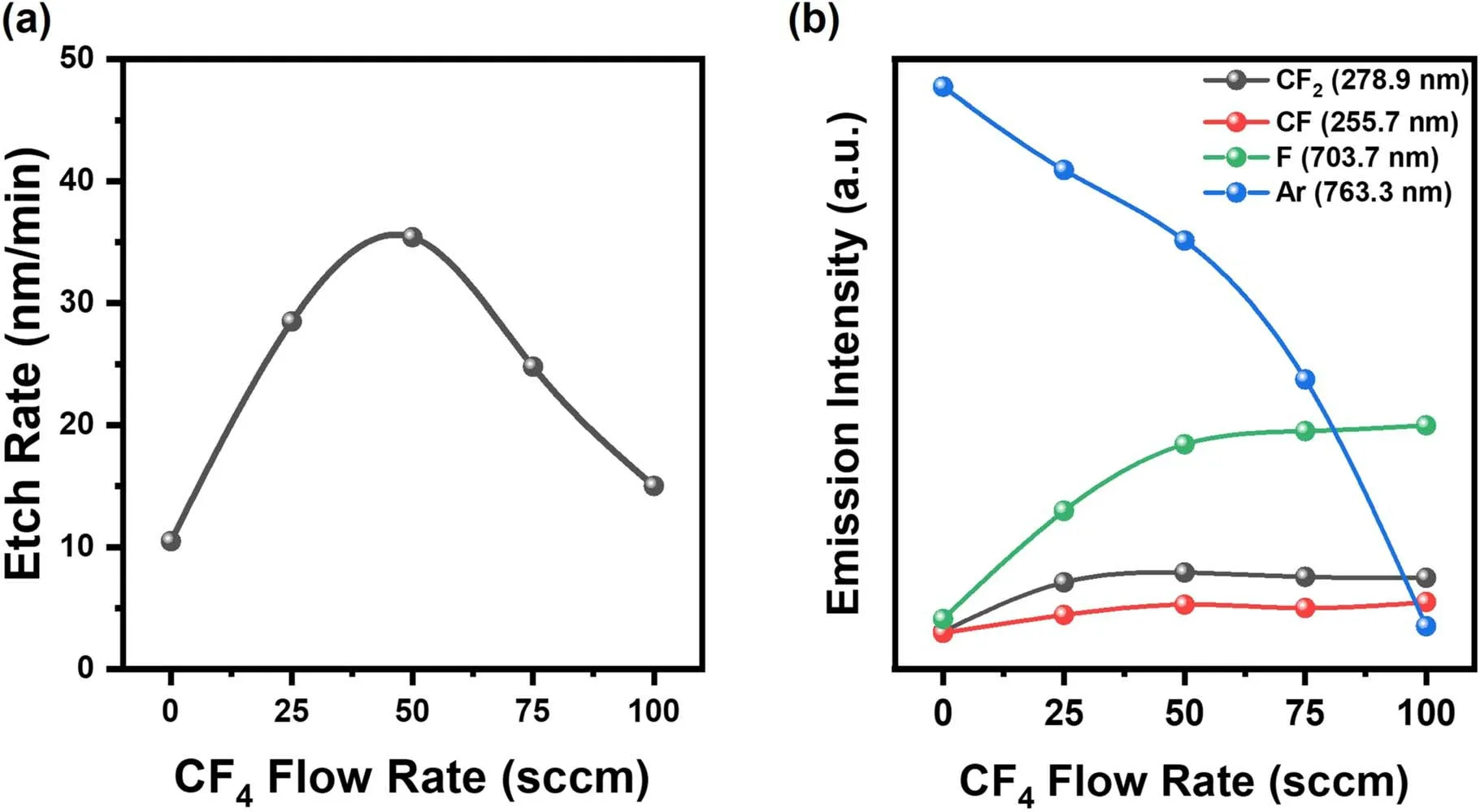
Figure 1.(a)Etch rate of AZO thin films and(b)OES analysis as a function of CF4 flow rate.Total gas flow rate(CF4+Ar)was 100 sccm.
Figure 1(a)shows that the etch rate of the AZO thin film increases from 10.13 to 36.2 nm min-1as the flow rate of CF4gas increases from 0 to 50 sccm in the CF4/Ar plasma.The etch rate decreased from 36.2 to 16.8 nm min-1as the flow rate of CF4increased from 50 to 100 sccm.As shown in figure 1(b),the emission of the F radical was most intense when the CF4flow rate was 100 sccm,whereas the emission of CF and CF2did not change significantly with variation in the flow rate of the CF4gas.After CF4/Ar plasma etching,the F components form non-volatile by-products,such as Al-F3(melting point:2250 °C)and Zn-F2(melting point:872 °C),on the surface of the AZO thin film.By-products with a high melting point remain on the surface of the AZO thin film and interfere with the etching process.These non-volatile byproducts are easily removed by Ar+sputtering.If the byproducts are not strongly bombarded by the Ar+ions,they remain on the surface of the AZO thin film.When the flow rate of CF4is more than 50 sccm,the etch rate is reduced because of the lower Ar+sputtering effect and increased production of F radicals.Therefore,increasing the number of chemical reactions does not affect the etch rate in the absence of strong ion bombardment.In addition,oxygen reacts with CF4plasma to generate volatile by-products(such as COF)[27].Consequently,etching is possible even when the flow rate of Ar is 0 sccm.The etch rate is maximal when the chemical reactions with CFxand F,and physical reactions such as Ar sputtering act simultaneously.
The change in the etch rate with variation in the other parameters is illustrated in figure 2.The CF4/Ar gas flow rate was fixed at 50/50 sccm for all conditions in figure 2.The correlation between the RF power and etch rate is shown in figure 2(a).The etch rate was measured by increasing the RF power in the range of 400–600 W.Bias power and process pressure were fixed at 150 W and 15 mTorr,respectively.As the RF power increased,the etch rate of the AZO thin film increased proportionally.Consequently,increasing the RF power increases the density of CFx,F radicals and Ar+ions in the plasma.Higher RF power creates more radicals that can reach the surface of the AZO thin film,increasing the chemical and physical reactions.Figure 2(b)shows the change in the etch rate of the AZO thin film according to the increase in bias power from 50 to 150 W.The RF power was 500 W and the process pressure was 15 mTorr.As the bias power increased,the etch rate increased dramatically.Bias power is a process variable that controls the average energy of Ar+ions participating in ion bombardment,which is a physical etching element,and the average energy of Ar+ions increases in proportion to the applied bias power.This means that the ion sputtering effect increases as the bias power increases.As the bias power increases,the etch rate increases since the surface residues are easily removed by Ar+sputtering.Figure 2(c)shows the change in the etch rate of the AZO thin film with variation in process pressure.The etch rate was measured by increasing the process pressure in the range of 10–20 mTorr.The RF power and bias power were 500 and 150 W,respectively.As the process pressure increases,the etch rate decreases.As the pressure increases,collisional recombination between particles increases.Consequently,the efficiency of the RF power is reduced[28].Moreover,the effect of physical sputtering decreases because the DC bias across the sheath decreases as the pressure increases.The reduction in these physical effects and chemical reactions leads to a decrease in etch rate at higher process pressure[29].
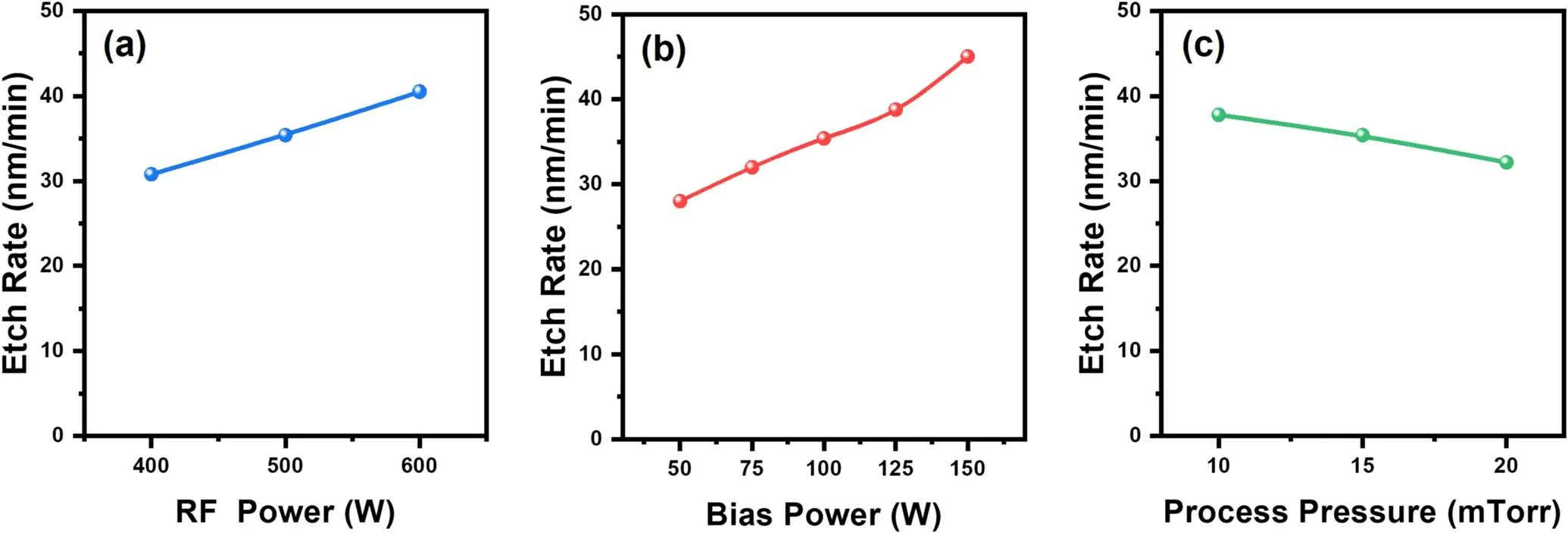
Figure 2.Etch rate of AZO thin film according to etch parameters of(a)RF power,(b)bias power and(c)process pressure.

Figure 3.XPS profiles of AZO thin film as a function of CF4/Ar gas ratio:(a)Al 2p,(b)Zn 2p(As-dep:before etching,CF4/Ar:after etching at CF4/Ar=50/50 sccm,CF4:after etching at CF4=100 sccm).
XPS was used to observe the change in the composition of the AZO thin film according to the flow rate of CF4gas.Samples were prepared under three conditions:(a)before etching,(b)after etching in CF4/Ar(=50/50 sccm)plasma and(c)after etching in CF4(=100 sccm)plasma.For the etch process,RF power,bias power and process pressure were fixed at 500 W,150 W and 15 mTorr,respectively.
Figure 3(a)shows the XPS narrow scan profile of the surface of the AZO thin film in the Al 2p region.The Al 2p peak is located at~73.95±0.1 eV,which corresponds to the characteristic peak of Al–Oxbefore CF4/Ar plasma etching.The peak of metallic aluminum at 72.7±0.06 eV did not appear in the XPS profile[30].As the flow rate of CF4increased,this peak was observed at 75.2 eV,related to Al–Fx[31].A comparison between the Al 2p profiles of the asdeposited and etched surfaces shows that the Al–Oxpeak became less intense in the case of the etched surface.This indicates that Al–Oxbonds are broken,Al reacts with F radicals,and O also reacts with F and CFxto form COF bonds.Figure 3(b)shows the XPS narrow scan profile of the Zn 2p peak.The two peaks at 1044.54 and 1021.32 eV are characteristic of the Zn 2p1/2and Zn 2p3/2states,respectively.After etching in CF4/Ar and CF4plasma,the Zn 2p peak was shifted by 1.3 and 1.4 eV towards higher BE,respectively(figure 3(b)).This BE shift is attributed to a change in the chemical binding state caused by the reaction of F and CFxradicals with Zn atoms on the surface of the AZO thin film.Because Zn binds more stably with F than with O(zinc fluoride ΔfGo=-713.3 kJ mol-1,zinc oxide ΔfGo=-320.5 kJ mol-1),the O atom is more likely to be substituted by F[32,33].
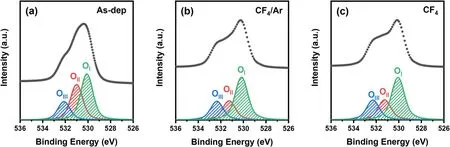
Figure 4.(a)–(c)O 1s XPS profile showing deconvoluted peaks of films etched with different CF4/Ar ratios(As-dep:before etching,CF4/Ar:after etching at CF4/Ar=50/50 sccm,CF4:after etching at CF4=100 sccm).
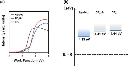
Figure 5.(a)UPS data for films etched with CF4/Ar plasma having different CF4 ratios,(b)variation in work function.
Figures 4(a)–(c)show the narrow scan spectra of the O 1 s region for the surface of the AZO thin film before and after etching in CF4/Ar and pure CF4plasma,respectively.For all samples,the O 1s peak was deconvoluted into three peaks.The low BE component centered at 530.1±0.2 eV is assigned to metal-oxide bonds(denoted as OI).The middle BE component centered at 531±0.2 eV is attributed to O vacancies(denoted as OII).The high BE component at 532.1±0.2 eV is assigned to hydroxyl(OH)on the surface of the AZO thin film(denoted as OIII)[34].When the flow rate of CF4was increased to 50 sccm,the intensity of the OIpeak first decreased,and increased again when the flow rate of CF4exceeded 50 sccm.This trend indicates that the metaloxide bonds are broken by Ar+sputtering,which increases the rate of the reaction of the F and CFxradicals with metal or O.The OIIpeak became less intense as the flow rate of CF4increased.F atoms can substitute oxygen or occupy oxygen vacancies in the ZnO structure.It is well known that F and O have a similar ionic radius,and the Zn–F bond is more stable than the Zn–O bond[35–37].The OIIIpeak first gained intensity and then became less intense as the flow rate of CF4increased.This is because the ratio of F present in the AZO thin film increases for the same reason as above.The F ion,which is the most electronegative ion,can also attract H atoms in the hydroxyl group that bind to the nearest O dangling bond to form an intermolecular F–HO H bond[35].Table 1 shows the atomic percentage and relative strength of the O 1 s peak.Table 1 shows that as the atomic percentage of F increased,the atomic percentage of O decreased.The detailed changes in the intensity of the OI,OIIand OIIIpeaks are presented in table 1.Through XPS analysis,it was confirmed that when the AZO thin film was etched using CF4/Ar plasma,Al–O and Zn–O bonds were broken and metal-F bonds were generated on the surface.It was also confirmed that F removed the O vacancies.
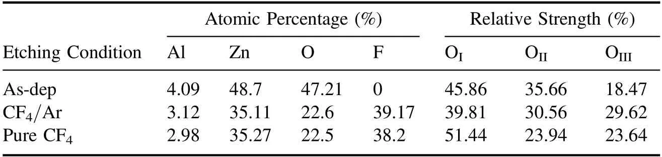
Table 1.Surface atomic percentage and relative strength of O 1 s.

Figure 6.(a)Transmittance and(b)optical bandgap energy of AZO thin film with increasing CF4 ratio in CF4/Ar plasma.
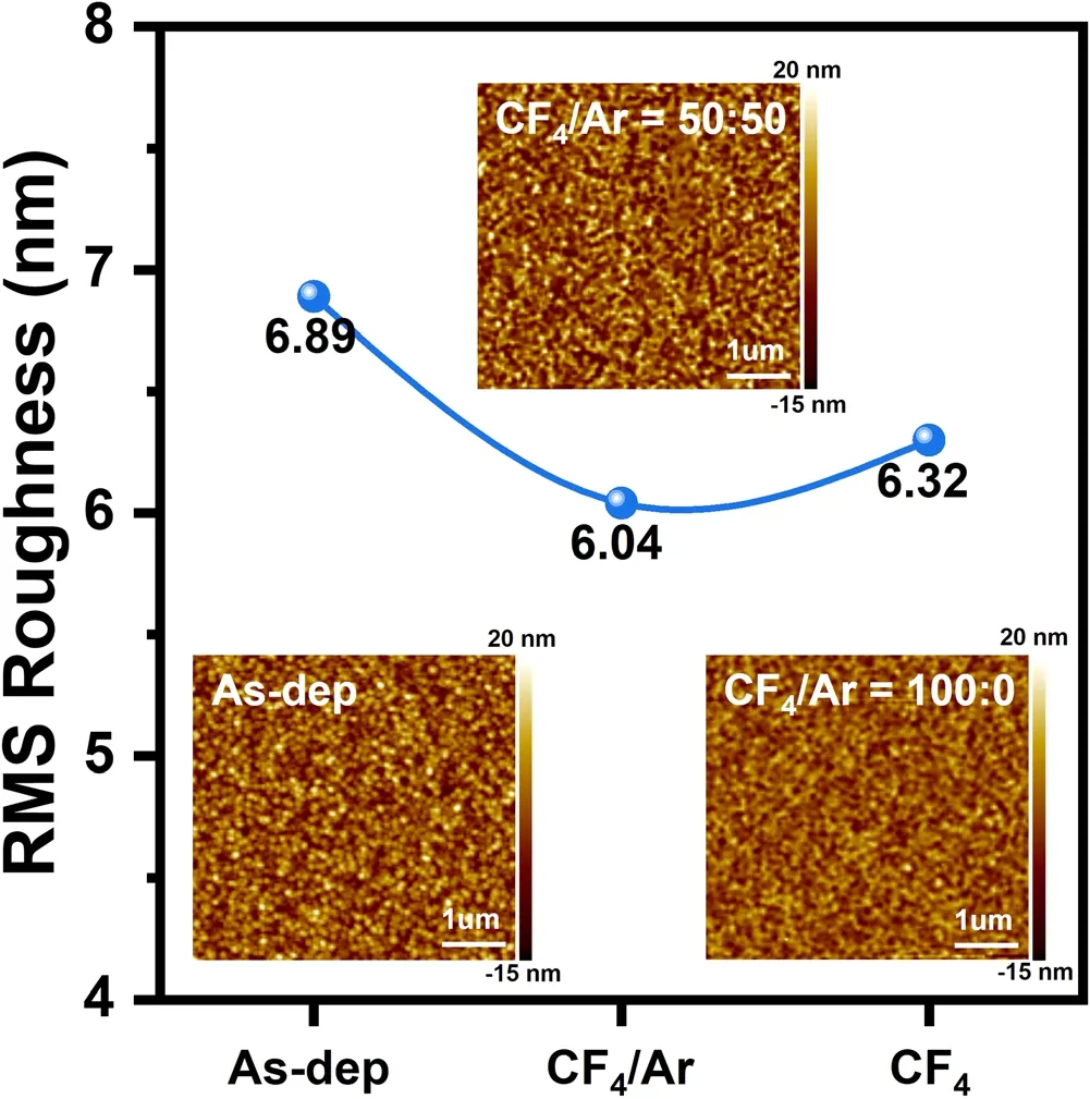
Figure 7.RMS roughness and AFM images of etched AZO thin film with CF4/Ar flow rate variation.
The change in the work function was measured using UPS analysis.Since it is very difficult to measure the Fermi edge of the oxide films,the work function was determined based on the Fermi level of Au,as a reference sample.The work function(Φ)was obtained according to equation(1).

Here,hvis the photon energy of the He I source(21.2 eV).EcutoffandEFrepresent the cutoff energy and Fermi-level energy,respectively.
Figure 5 shows the changes in the work function(from the UPS data)with variation in the flow rate of CF4gas.The work function increased from 4.19 to 4.44 eV as the flow rate of CF4gas increased.The CF4plasma affects the formation of F radicals and metal bonds on the surface of the AZO thin film and reduces the number of O vacancies.This reaction contributed significantly to the change in the work function.Moreover,free electrons may be generated by replacing O ions with F ions because of the difference in the electrovalency of the O ionsand F-ions(see equation(2))[32].
Therefore,the electron concentration of AZO increased,shifting the Fermi level to the conduction band,and the work function also increased.
Figure 6 shows changes in the transmittance spectra with variation in the flow rate of CF4gas.Figures 6(a)and(b)show the transmittance and optical bandgap energy,respectively.In figure 6(a),the transmittance in the visible light region is maintained at 80% or more even after plasma etching.The optical band gap can be determined from the transmittance spectra.The optical band gap was calculated using the tauc equation(equation(3)).
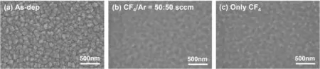
Figure 8.FE-SEM images of AZO thin film before and after plasma etching under CF4/Ar flow rate variation.
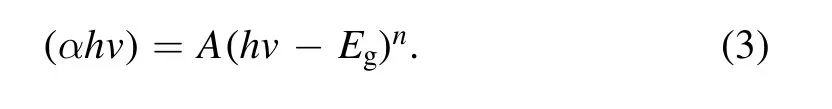
Here,α is the absorption coefficient,Ais a proportionality constant,Egis the band gap of the material,andndepends on the type of transition.The optical bandgap energy of the AZO thin film in the‘As-dep’sample was 3.46 eV.As the flow rate of CF4gas increased,the bandgap energy increased by 0.06 eV(from 3.46 to 3.52 eV).The optical bandgap energy appeared to increase due to a reduction in the number of O vacancies by F radicals on the AZO surface.
The surface roughness of transparent conductive thin films is an important feature for many applications and is well known to have a significant impact on device performance[38].Therefore,it is important to measure the surface roughness of the AZO thin film after plasma etching.
Figure 7 shows the surface roughness of the AZO thin film with variation in the flow rate of CF4gas.After etching with CF4/Ar plasma,the roughness of the film was reduced under all conditions compared to that of the As-dep thin film.In the CF4/Ar plasma,the AZO thin film is etched by the sputtering effect and chemical reaction,resulting in reduced surface roughness.In addition,as the flow rate of CF4increased,the surface roughness appeared to increase due to an increase in the amount of by-products on the surface of the AZO thin film.
Figure 8 is an FE-SEM image of the surface of the AZO thin film before and after plasma etching.The surface of the AZO thin film is changed and becomes smooth after plasma etching.In particular,it is confirmed that the surface of the AZO thin film etched at the CF4/Ar ratio of 50:50 is the smoothest.This result supports the change in surface roughness after etching using AFM analysis.
4.Conclusion
This study shows the etching characteristics and surface properties of AZO thin films in CF4/Ar plasma.The highest etch rate was achieved with a CF4/Ar ratio of 50:50 sccm.When the flow rate of CF4gas exceeded 50 sccm,the etch rate decreased because the non-volatile by-products generated on the AZO surface increased as the flow rate of CF4gas increased,and the Ar sputtering effect decreased.Thus,the by-products were not easily removed.XPS analysis demonstrates that when the AZO thin film is etched using CF4/Ar plasma,metal-F bonds are formed by the F radicals to generate a non-volatile by-product.Moreover,the F ion replaces the O ion to create a free electron in the AZO thin film.This causes an increase in the work function and bandgap energy from 4.19 to 4.44 eV and 3.46 to 3.52 eV,respectively.In contrast,after plasma etching,the surface roughness decreased under all conditions,where the minimum roughness was 6.04 nm.
Acknowledgment
This work was supported by the National Research Foundation(NRF)of Korea(Nos.2018R1D1A1B07051429 and 2020R1G1A1102692).
 Plasma Science and Technology2022年7期
- Plasma Science and Technology的其它文章
- Special issue on selected papers from CEPC 2021
- Highly efficient γ-ray generation by 10 PWclass lasers irradiating heavy-ion plasmas
- Photoexcited carrier dynamics in a GaAs photoconductive switch under nJ excitation
- Molecular mechanism study of Astragalus adsurgens Pall synergistically induced by plasma and plasma-activated water
- Microwave method based on curve fitting method for high-precision collision frequency diagnosis
- Inverse synthetic aperture radar range profile compensation of plasma-sheathenveloped reentry object