
A high rectification efficiency Si0.14Ge0.72Sn0.14–Ge0.82Sn0.18–Ge quantum structure n-MOSFET for 2.45 GHz weak energy microwave wireless energy transmission
2022-06-29 08:56:40DongZhang張棟JianjunSong宋建軍XiaohuanXue薛笑歡andShiqiZhang張士琦
Chinese Physics B 2022年6期
關(guān)鍵詞:建軍
Dong Zhang(張棟) Jianjun Song(宋建軍) Xiaohuan Xue(薛笑歡) and Shiqi Zhang(張士琦)
1School of Microelectronics,Xidian University,Xi’an 710071,China
2Radiation Resistant Integrated Circuit Technology Laboratory of China Aerospace Science and Technology Group Corporation,Xi’an 710071,China
Keywords: microwave wireless energy transmission,quantum structure,GeSn,MOS rectification
1. Introduction
In a microwave wireless energy transmission system(MWETS), power is transferred by radio frequency (RF) energy beams to give a direct current (DC) without a transmission line. Such a system can be used in wireless sensor networks and radio frequency identification systems as the power supply generator instead of using a wired power supply and battery.[1–3]The most important part of this system is the RF to DC voltage converter circuit(rectifier circuit)and the rectifier device is the core of the circuit. At present,popular rectifier devices are the Schottky diode and complementary metal–oxide–semiconductor (CMOS) devices. The advantages of a Schottky diode are its low turn-on voltage and the simple manufacturing process.[4]However,Schottky diodes are not compatible with the CMOS process and show a low rectification efficiency under weak energy conditions.In contrast,MOS devices can be integrated into a circuit using the mature CMOS process. However, due to the larger internal loss caused by the complexity of the structure compared with the Schottky diode,a special design is required to improve the rectification efficiency under weak energy conditions.
Current work is focused on the design and implementation of an optimized CMOS rectifier with good efficiency in a MWETS because of the compatibility of the bulk silicon process. However, most attention is paid to circuit optimization rather than improving the characteristics of the device.A review[5]has concluded that it is possible to design highperformance devices compatible with the CMOS process by changing materials such as Ge and setting a reasonable device structure.
Direct band gap germanium–tin (DR-Ge1-xSnx) material has a higher electron mobility than Ge, and its band gap can be adjusted by changing the Sn content.[6–8]By adjusting the band gap of Ge1-xSnxand silicon–germanium–tin(SiyGe1-y-zSnz) to form a SiyGe1-y-zSnz/DR-Ge1-xSnx/Ge quantum well structure,channel scattering can be reduced and the channel mobility of the device can be further improved.
Using the SiyGe1-y-zSnz/DR-Ge1-xSnx/Ge quantum well structure as our basis, in this work we design a quantum structure n-MOS device that can be used for 2.45 GHz weak energy microwave wireless energy transmission. First,a SiyGe1-y-zSnz/DR-Ge1-xSnx/Ge quantum structure n-MOS device is designed based on the characteristics of Ge1-xSnxmaterials. Then its threshold voltage andI–Vcharacteristics are analyzed using simulation. Finally, a simple half-wave rectifier circuit is built using the mixed-mode mode of Silvaco TCAD software, and the rectification characteristics of the quantum structure device and the Si n-MOS device are compared.
2. The n-MOS design
The key to the design of a SiyGe1-y-zSnz/DRGe1-xSnx/Ge quantum well structure for an n-MOS device is to adjust the content of Si and Sn in SiyGe1-y-zSnzand the content of Sn in DR-Ge1-xSnxto form a deep band offset of the conduction band(ΔEc). In this way,the electrons are confined in the quantum well (DR-Ge1-xSnxchannel layer) and the influence of the surface cap layer is suppressed due to the Fermi pinning effect of the SiyGe1-y-zSnzalloy with a high Ge content.
2.1. Physical design of layer structure material
The electron and hole mobilities of Ge material are superior to Si, and therefore it can be regarded as a substitute for Si. However, the disadvantage of Ge is that its band gap is narrow and its thermal stability is not as good as that of Si. At the same time, due to the Fermi pinning effect of Ge materials and the low activation concentration of n-type impurities,production of a Ge n-MOS can be problematic.[5]
Ge–Sn material has higher electron and hole mobilities than Ge. By adjusting the Sn doping,indirect band gap Ge–Sn can be converted to direct band gap Ge–Sn to improve the electron mobility. Also, the introduction of Si–Ge–Sn can allow formation of a heterojunction structure with Ge–Sn,making it possible to produce a Ge-based n-MOS device.

whereEgGe,EgSiandEgSnare the band gaps of Ge,Si and Sn,respectively, andbGeSi,bGeSn, andbSiSnare the band bowing parameters corresponding toΓorLvalleys which were calculated in Ref.[15]. The values are shown in Table 1.


bGeSi bGeSn bSiSn EgGe EgSi EgSn L-valley 0 -0.11 0 0.66 2 0.14 Γ-valley 0.21 1.94 13.2 0.795 4.06 -0.413
The bottom of the conduction bands for Ge1-xSnxand SiyGe1-y-zSnzcan be deduced from the above relationships. On this basis, figure 1(a) shows the band structure of Ge1-xSnx. The relationships between the lattice constants of Ge1-xSnxand SiyGe1-y-zSnzare

whereais the lattice constant. Therefore, lattice matching between Ge1-xSnxand SiyGe1-y-zSnzcan be achieved by adjusting the content of SiyGe1-y-zSnz, as shown in Fig. 1(b).With increasing Sn content in Ge1-xSnx, the proportional range of lattice-matched SiyGe1-y-zSnzalloy is wider. Considering the requirement of ΔEcfor formation of a quantum well, it is appropriate to take the Sn content in Ge1-xSnxas 0.18,and the conduction band offset ΔEcis 0.116 eV relative to the bottom of the conduction band for Ge.
The variation trend of the SiyGe1-y-zSnz–Ge0.82Sn0.18band offset with SiyGe1-y-zSnzcomposition is shown in Fig. 1(c). Considering lattice matching and band offset, Si0.14Ge0.72Sn0.14and Ge0.82Sn0.18are used to form a Si0.14Ge0.72Sn0.14–Ge0.82Sn0.18–Ge double heterojunction structure.As shown in Fig.1(d),in the above structure ΔEcbetween Si0.14Ge0.72Sn0.14and Ge0.82Sn0.18is 0.203 eV and ΔEvbetween them is 0.113 eV. Meanwhile, ΔEcbetween Ge and Ge0.82Sn0.18is 0.116 eV and ΔEvbetween them is 0.253 eV.The above data show that a good quantum structure is formed.
2.2. Electron mobility calculation
The energy band structure of DR-Ge1-xSnxis different from that of Ge. The Sn composition makes the effective mass of this alloy smaller than that of Ge, so that its mobility is greatly improved relative to Ge. However,the solid solubility with a high Sn content will cause disordered scattering of the alloy,resulting in a decrease in mobility,and the proportion of Sn will also affect the mobility.[11]The formula for mobility calculation is
whereμnis the electron mobility,m*nis the effective mass of the electron andτnis the electron mean free time. Considering that the electron scattering mechanism in DR-Ge1-xSnxis mainly ionized impurity scattering(Pe,//),acoustic phonon scattering (Pe,ac) and alloy disorder scattering (Pe,ad), the following relationships between scattering and electron mean free time are obtained:
Therefore,the electron mean free time is given by

Combining the above analysis and literature data,[11]the change in bulk material mobility with Sn composition can be calculated(Fig.2). The electron mobility of bulk materials increases with increase in the Sn content,and its value is as high as 1.75×104cm2/(V·s) whenx=0.18. However, this is an ideal value. In actual devices,the energy band structure of the channel layer, the influence of the mobility between different energy valleys of Ge1-xSnxand the influence of the quantization effect in the device all need to be considered.[16]For DRGe1-xSnx, limitedΓ-valley occupied electronic energy rates and the impact of mobility in theL-valley cannot be ignored.Figure 2 also indicates that the average electron mobility andΓ-valley electron mobility of the device both increase with increase in the Sn content. From this figure,wherex=0.18,the average electron conductance mobility of the channel is about 1.67 times that of Ge,namely,6333 cm2/(V·s)as used in the simulation.

2.3. Design of the device structure
At present, the research on quantum structure MOS devices is mostly focused on SiGe materials, rarely on GeSn materials. It is easy for parasitic channels to form with a Si cap layer on a quantum structure metal–oxide–semiconductor field-effect transistor (MOSFET). At the same time, due to the inherent characteristics of Ge, it is difficult for a P-type substrate to generate an N-type surface channel, so a highperformance Ge-based n-MOS is extremely difficult to manufacture. The quantum well structure described in this paper can effectively avoid these problems.
In this paper,the following quantum structure n-MOS device is designed based on the structure discussed in Subsection 2.1. With regard to process compatibility, a Ge epitaxial layer was deposited on a Si substrate, and a high-quality virtual Ge substrate was formed by laser recrystallization. The channel and doping of the device are separated by depositing aδ-doping layer on the virtual substrate,and the scattering of ionized impurities is effectively reduced, thus improving the mobility. At the same time,the threshold voltage of the device can be adjusted by controlling the doping concentration of the doped layer. Then,the DR-Ge0.82Sn0.18channel layer and the Si0.14Ge0.72Sn0.14cap layer are deposited, thus forming the Si0.14Ge0.72Sn0.14–Ge0.82Sn0.18–Ge quantum structure. The channel carrier concentration can be controlled by the MOS structure on the top,thereby controlling whether the device is on or off. The Fermi pinning effect of the cap layer of high Ge content alloy Si0.14Ge0.72Sn0.14can be used to suppress the formation of surface parasitic channels to improve the performance of the device. Finally, Al or Ni is used to anneal the source and drain to form ohmic contacts. Figure 3 plots the structure of the above MOS device and shows parameters that will be used in the simulation.

2.4. Simulation of band characteristics
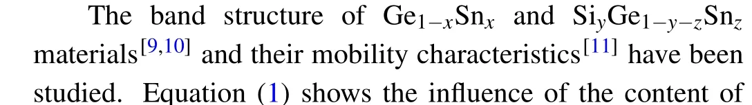
To obtain the energy band characteristics of the device,simulations were performed using Silvaco TCAD software;the model structure is shown in Fig.4. The entire device channel length is 400 nm,and some process technologies were not considered in order to simplify the analysis and improve the simulation speed. The vertical energy band image(forx=0)is obtained by taking the oxide–cap interface as the reference interface. From Fig. 5(a), it can be seen that the bottom of the conduction band is bent at the cap–channel interface and the cap–oxide interface. Although the bottom of the conduction band at the cap–oxide interface is lower than that at the cap–channel interface,electrons do not accumulate at the surface due to the fact that high-Ge alloys are difficult to invert to form N-channels. As a result, electrons accumulate near the interface between the channel and the cap layer(closer to the Ge0.82Sn0.18channel layer side)to form a conductive channel.
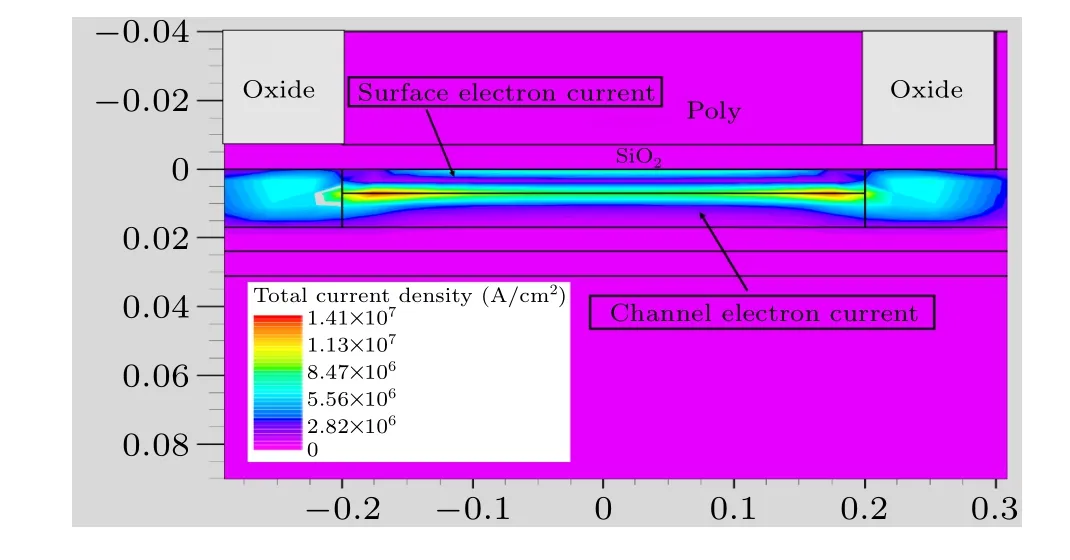
The diagram of the longitudinal distribution of the electron current density (Fig. 5(b)) also verifies the above analysis; it can be seen that the maximum electron current density in the vicinity of the channel and cap layer is 340000 A/cm2at a gate voltage of 2 V,while the electron current density at the top surface of the cap layer is less than 20000 A/cm2, which is nearly 17 times smaller than the peak current density at the channel. On the one hand,this indicates that the device is indeed an n-MOS device and the vast majority of the electron current is confined inside the quantum well channel because the surface channel is suppressed. On the other hand, the intrinsic Ge layer isolates the dopant layer and the channel layer,thus avoiding any influence of the dopant layer on the electron current.

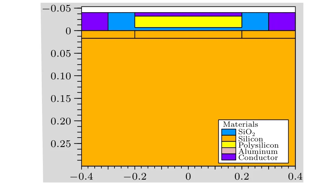
This is further verified by the two-dimensional device distribution of the electron current density with a 2 V gate voltage(Fig. 6), which clearly shows that the electrons are confined inside the quantum well with the peak close to the cap layer,and the current density gradually decreasing to both sides; it is therefore reasonable to place the dopant layer on the lower side of the channel layer and set the isolation and cap layer to reduce scattering.At the same time,the surface channel is also clearly suppressed. This fully demonstrates the superiority of the quantum well structure device. The structure of a Si MOS device is shown in Fig.7 for comparison.
3. The n-MOS characterization
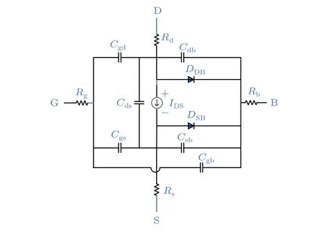
The quantum structure n-MOS mentioned in this paper is similar to bulk Si devices with the characteristics of both MOSFETs and modulation-doped field-effect transistors, and various small-signal models for quantum well devices are given in Refs. [17–20]. A small-signal model is considered in conjunction with the literature above and as shown in Fig.8 for subsequent analysis. The device model is similar to a Si MOS device,with differences in threshold voltage and capacitance structure. For this quantum well structure, the threshold voltage of this device consists of the quantum well channel threshold voltage and the surface parasitic channel.[21–25]However,due to the SiGeSn cap layer having a high Ge content,the Fermi level is pinned at the interface between the cap layer and the oxide layer,making the surface parasitic channel threshold voltage much higher than the quantum well channel threshold voltage. In a weak energy density harvesting circuit the surface parasitic channel can be neglected because the gate voltage is low (much less than 1 V). In addition, unlike the MOS structure, the heterojunction capacitance between different epitaxial layers should be considered for this device in addition to the MOS gate oxide capacitance.
3.1. Threshold voltage calculation and simulation
For MOS devices, the threshold voltage is an important parameter whose value is related to the gate oxide thickness,the gate electrode work function and the device doping concentration.Also,for a diode connection MOSFET device used in rectification,it is effective to reduce the turn-on voltage(the threshold voltage of the MOS device)to improve the rectification efficiency.According to the literature,[2,3]the rectification efficiency of MOS devices can be improved by using very low threshold voltages. It is necessary to analyze the threshold voltage formula for the device. For a quantum structure device it is assumed that theδ-doped layer is fully depleted and the remaining charge required for the channel comes from the substrate layer.
Assuming that the charge density at theδ-doping layer isQm,the relationships through each layer have the form of the Poisson equations[22,25]shown in Fig.9,which are solved for when the gate voltage is lower than the threshold voltage to give the following equation:

whereNB1is the substrate doping concentration,R1is equated toεge/εgesnandεge,εgesnandεsigesnare the material dielectric constants. For GeSn alloys with a high Ge content,R1is approximated as 1. Based on Eqs. (7) and (8), the threshold voltage for the n-MOS device in this paper is given by
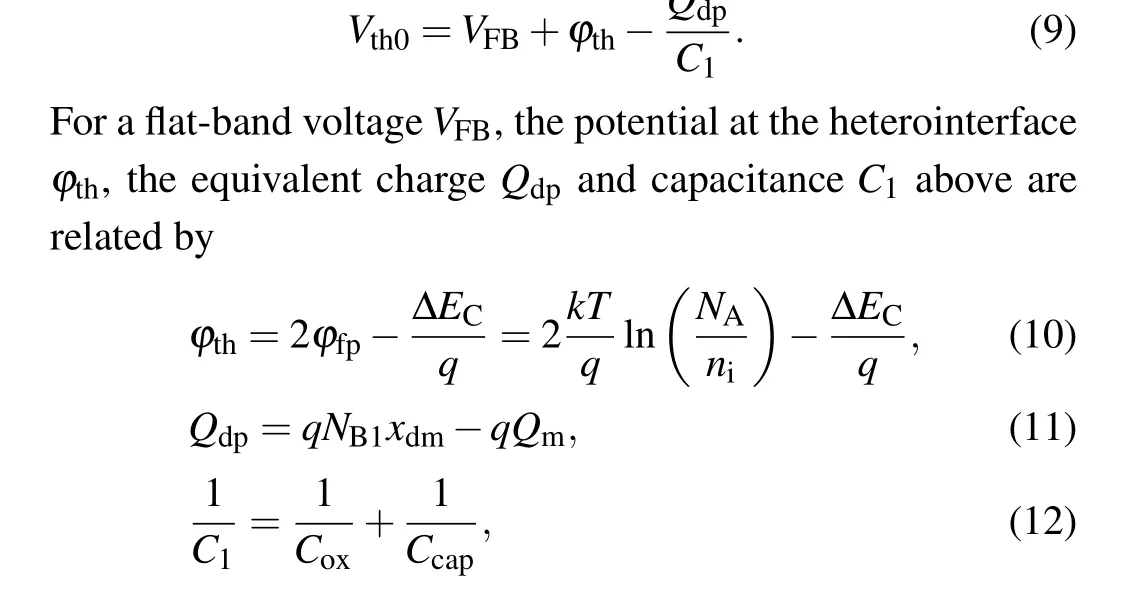
whereφf(shuō)pis the Fermi potential,Coxis the gate oxide capacitance andCcapis the cap capacitance. The above equations solve for the channel threshold voltage,and it can be seen that the threshold voltage of the device introduces the conduction band offset ΔECand the heterojunction structure capacitance compared with the equation for calculating the threshold voltage of a Si MOS device. Therefore, according to the above equations, the threshold voltage can be adjusted by changing the process parameters such as layer structure parameters and theδ-doping layer concentration of the device.

The variation of the threshold voltage of the device with the doping concentration of the doping layer is shown in Fig. 10(a) as an orange solid line. It is easy to observe from the figure that the threshold voltage of the device increases with increase in the P-type impurity doping concentration of the doped layer, and especially between 1018cm-3and 1019cm-3,mainly due to the increase inφthas shown in Eq.(10).
It can be seen from Fig. 10(a) that the variation of the threshold voltage with the thickness of cap layer is different from that of the other layers. The electron longitudinal current density diagram in Fig. 10(b) can explain this phenomenon.As the thickness of cap layer increases, the current density of the parasitic channel gradually increases,while the current density of the DR-GeSn channel gradually decreases;together these have an effect on the threshold voltage. When the thickness of cap layer increases to 10 nm,the peak electron current density of the cap layer is higher than the peak electron current density of the channel, which means that the threshold voltage is dominated by the cap layer and the cap layer parasitic channel opens before the quantum well channel. Notice that the sum of the electron current densities of the cap layer and quantum well channel attcap=1 nm is much larger than that at 6 nm and 10 nm,which also explains why the threshold voltage is lower when the cap layer is extremely thin. Considering the process compatibility,it is more reasonable to take 6 nm as the cap layer thickness.
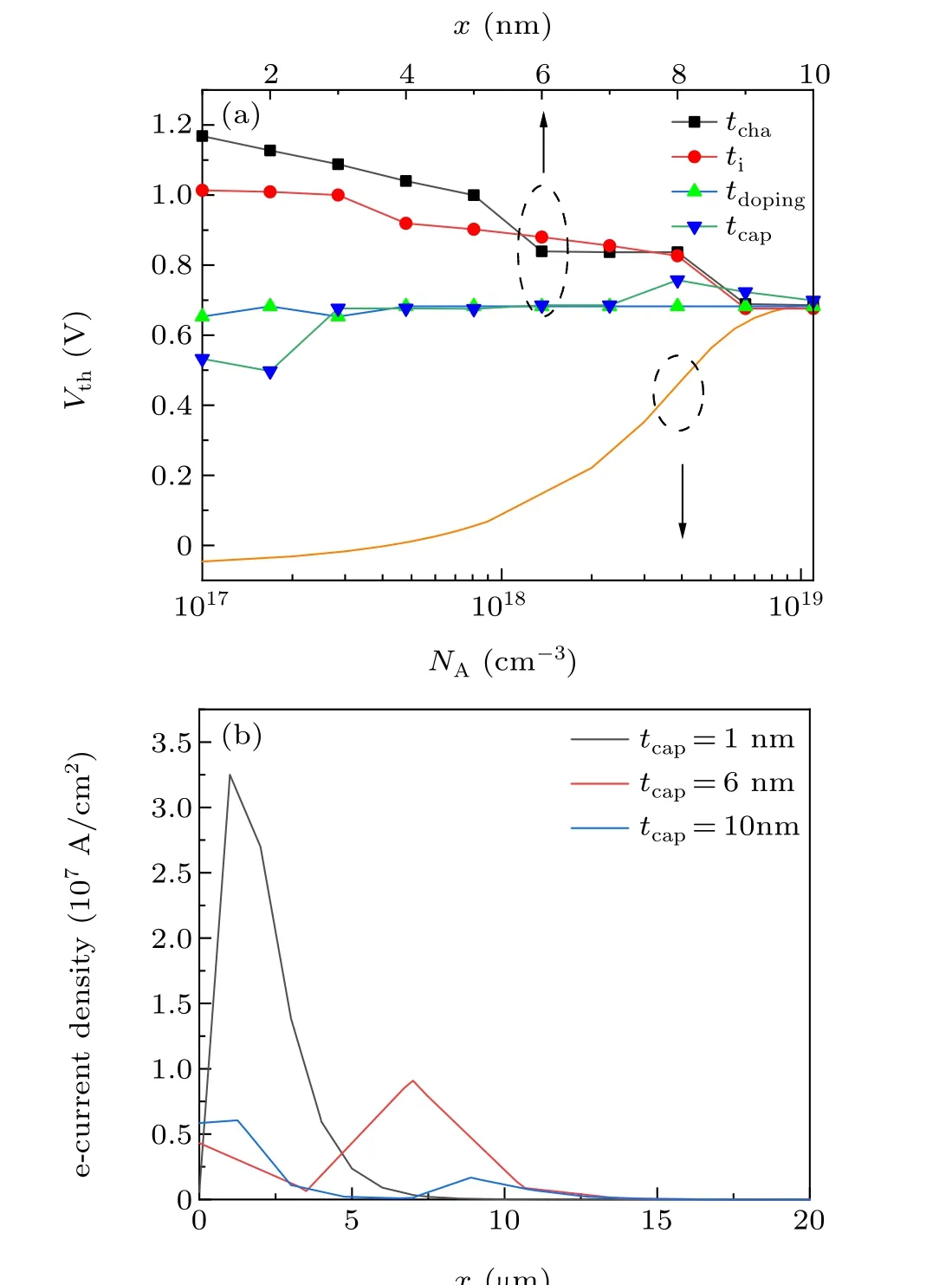
The influence of channel layer thickness, buffer layer thickness and dopant layer thickness on the threshold voltage is also shown in Fig.10(a). As the channel layer thickness and buffer layer thickness increase,the threshold voltage gradually decreases, while the dopant layer thickness has less effect on the threshold voltage. A comprehensive analysis of the thickness parameters of each channel layer was shown in Fig.7.
Comparison of Figs. 10(a) and 10(b) shows that the threshold voltage is more sensitive to the dopant layer concentration. Therefore,by adjusting the dopant layer concentration to 1018cm-3,a threshold voltage of 91 mV is obtained in order to improve the rectification efficiency of the device.
3.2. The I–V characteristics

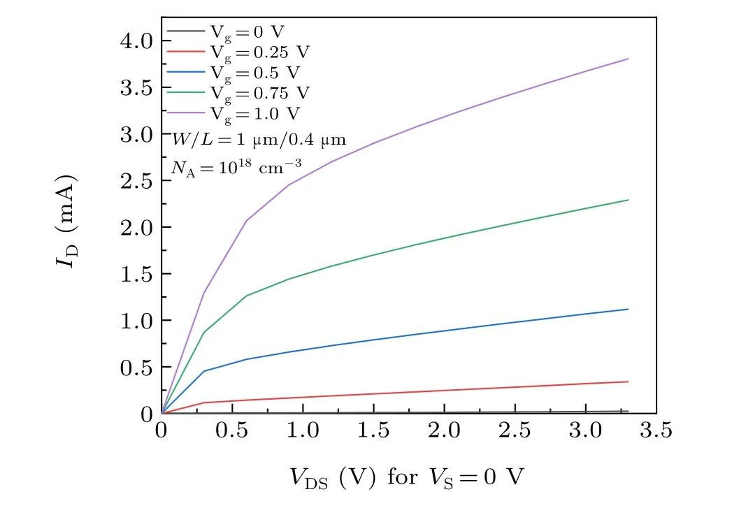
The transfer and output characteristics of the device are shown in Figs. 11 and 12. The transfer characteristics atVDS= 0.1 V for doping concentrations of 1019cm-3and 1018cm-3, respectively, are shown, and it can be seen that whenW/L=1 μm/0.4 μm,the current is up to the mA level atVg=1 V, which is an advantage of the high mobility due to the quantum wells.The threshold voltage varies at different doping concentrations,as can be seen at 1019cm-3,the curve shifts left relative to 1018cm-3and the threshold voltage decreases, which is beneficial for rectification applications.However,it also results in a larger leakage current and poorer subthreshold characteristics of the device. The output characteristics further demonstrate the excellent performance of the device and also show the effect of the channel length,which is very obvious whenVgis above 0.5 V.
4. Principles of rectifier circuit design and circuit simulation
In this paper, in order to analyze the effect of quantum channel devices on rectification and energy harvesting,a halfwave rectification circuit as in Fig. 13 is briefly considered.The device is connected like a diode, an AC current source with 50 Ω internal resistance is used as the power input,a load capacitorC1is used to stabilize the DC output waveform and the resistorR1is the output load.

There are two types of connections for a MOS used for rectification,[2,3]one is the conventional diode connection
where the source and gate are connected as input and the source and substrate are connected as output and the other is the novel connection where the substrate, drain and gate are connected as input and the source is set as output. As the source and substrate potential of the novel connection is not zero,according to the threshold voltage Eq.(13),VSBhas a modulating effect on the threshold voltage. When a forward voltage is applied,which effectively reduces the forward turn-on voltage, the forward conduction current is greatly increased.When a reverse voltage is applied,the reverse leakage current is greatly reduced, helping to eliminate the problems of a high leakage current with a low threshold voltage, thus effectively improving the efficiency of the rectifier circuit[2]Equation (13) still applies for the quantum structure device,whereVth0is the intrinsic threshold voltage described in Subsection 3.2 andΦFis the Fermi potential of the device herein.
4.1. DC simulation
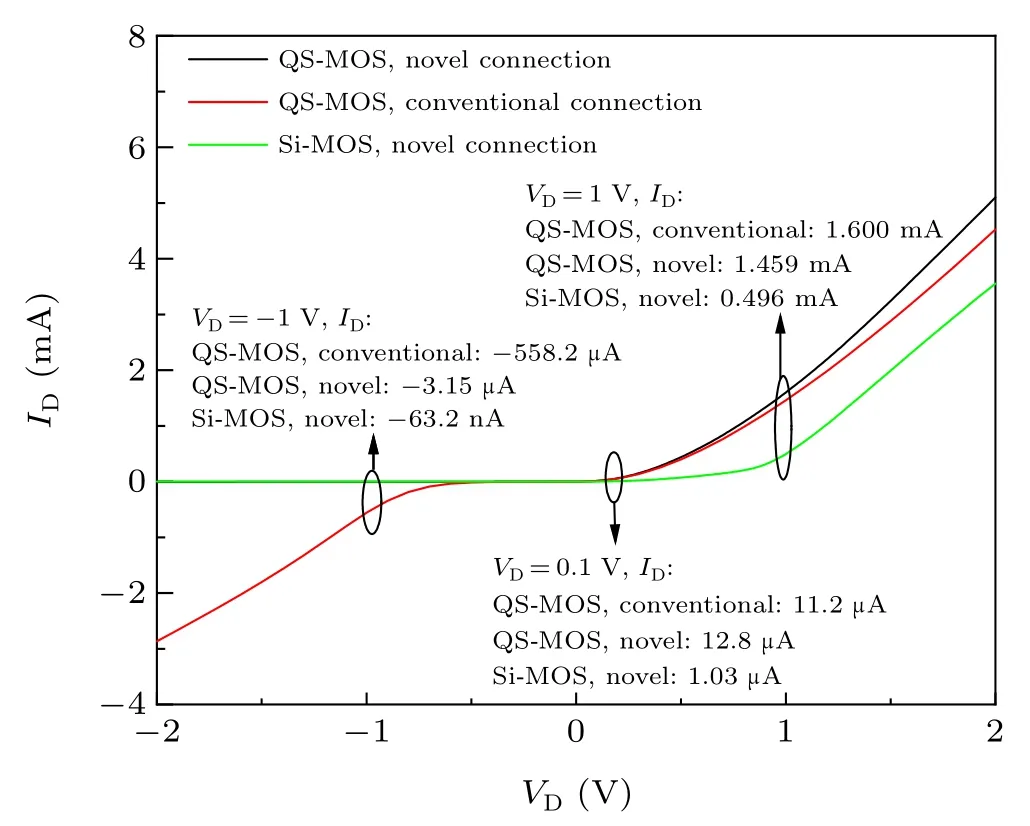
Figure 14 compares theI–Vcurves of the two connection methods for the quantum structure MOS device(QS-MOS in the figure). It can be seen that in forward bias the two curves almost coincide in the 0 V–0.5 V interval,and the novel connection has a higher current in the region above 0.5 V. However, in reverse bias, the conventional connection has a significantly higher breakdown current than the new connection,with a difference of 177.2 times between them at-1 V for example. This shows that the substrate bias can effectively improve the subthreshold characteristics of the quantum structure device and greatly reduce the leakage current.
Also, comparing the Si MOS and the quantum structure device using the new connection method, the current of the quantum structure device is significantly larger than that of the Si MOS at forward bias in the figure. Although the leakage current of the Si MOS device is lower in the reverse bias case,indicating that the loss of rectification of this quantum structure device may be higher than that of the Si MOS device,the high current characteristic due to the high electron mobility makes the rectification effect of this device much better than that of the Si MOS.

4.2. TRAN simulation
An important indicator for AC–DC conversion circuits is the rectification efficiency, which characterizes the energy conversion efficiency of the circuit. The formula for rectification efficiency is
Based on these relationships, the instantaneous input power and output power variation curves for the circuit can be plotted(Fig.15(c)). According to the above instantaneous power analysis, the rectification efficiency within one cycle can be solved as
The above conditions are analyzed and simulated to obtain the rectification efficiency and output voltage curves under different loads,as shown in Fig.15(d). In order to have a balanced performance of output voltage and rectification efficiency, a load resistor of 20 kΩ is chosen.
Figure 16 compares the variation of the rectification efficiency between the Si MOS and the quantum MOS under the same conditions as mentioned before. It can be seen that the quantum MOS has a better conversion efficiency relative to the Si MOS in the input power range of-30 dBm to 6.9 dBm. At an input power of-10 dBm,the efficiency of the quantum device can reach 7.14%,which is 4.2 times that of the Si MOS.There is a peak conversion efficiency of 45.51% at 6.9 dBm,which is still higher than that of the Si MOS(42.13%). However,above 6.9 dBm,the rectification efficiency of the device decays rapidly and the rectification effect is weaker than that of an ordinary Si MOS. Comparison shows that their output voltages are similar. Below an input power of 10 dBm, the output voltage curve of the quantum MOS is higher than that of Si MOS, while above 10 dBm it decays rapidly. In short,this figure shows that the quantum MOS has a better weak energy density collection capability at 2.45 GHz relative to the Si MOS under the same conditions.
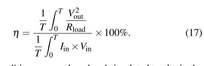
Comparing the efficiency curves at different widths(Fig. 17), it can be seen that as the width increases the peak rectification efficiency first increases,reaching a peak of 48.52%atW=2.5 μm,and then gradually decays. When the width is greater than 2.5 μm,there is a significant overall decay in the efficiency curves and the maximum efficiency drops rapidly.For a CMOS rectifier circuit,a width of 2.5 μm means that the area of a single device can be reduced by several times,which greatly reduces the area of the chip and cuts the cost.

5. Conclusion and perspectives
In conclusion, a quantum structured n-MOS device was designed using SiGeSn and GeSn materials,which greatly improved the mobility of the device compared with ordinary Si devices. The threshold voltage and electrical characteristics of the device were analyzed by simulation. In order to improve the rectification efficiency,the threshold voltage of the device was adjusted to 91 mV, and a simple half-wave rectification test circuit was built with a novel connection method. The advantages of this MOS over a Si MOS were analyzed in terms of DC and transient simulation,and a rectification efficiency of 7.14%(at-10 dBm)was obtained,which is 4.2 times higher than that of a Si MOS under the same conditions, fully illustrating the advantages of this device.
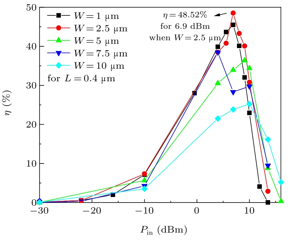
Table 2 compares the results of this work and some previous works,[3,28–31]showing the advantages of the device described this work. It is worth noting that for simplicity of analysis the device modeling in this paper does not take into account the various process designs in the short channel case,and the device feature size is 400 nm. Therefore, it is believed that with process improvement such as advanced nodes,proper matching and boost circuit design as summarized in the Ref.[28], the device described in this paper will be more advantageous in the RF rectification field.
Ref. Tech. Rectifier topology Frequency(GHz) Power conversion efficiency(%for load at input level)This work 400 nm n-MOS one-stage half-wave 2.45 7.14%for 20 kΩ@-10 dBm[3] 180 nm CMOS five-stage on-chip inductor 0.9 14.46%for 200 kΩ@-9 dBm[29] 300 nm CMOS three-stage Dickson 0.95 1.5%for 200 kΩ@-14 dBm[30] 90 nm CMOS four-stage Dickson 2.45 1%for 1 MΩ@-8.06 dBm[31] 180 nm CMOS five-stage Dickson 2.63 7%for 500 kΩ@-15.4 dBm
Acknowledgments
Project supported by the National 111 Center (Grant No. B12026) and Research on *** Technology of Intelligent Reconfigurable General System(Grant No.F020250058).
猜你喜歡
環(huán)球時(shí)報(bào)(2022-08-02)2022-08-02 22:41:57
Chinese Physics B(2022年6期)2022-06-29 08:52:52
Acta Mathematica Scientia(English Series)(2022年1期)2022-03-12 10:21:40
Plasma Science and Technology(2021年2期)2021-02-27 09:16:58
江蘇教育·書法教育(2020年10期)2020-09-10 07:22:44
當(dāng)代人(2020年4期)2020-05-08 08:18:04
中華魂(2017年8期)2017-11-22 12:21:09
綠色中國(guó)(2017年15期)2017-01-25 08:55:36
水動(dòng)力學(xué)研究與進(jìn)展 B輯(2015年3期)2015-02-16 06:50:29
外科研究與新技術(shù)(2012年1期)2012-08-15 00:54:32
- Chinese Physics B的其它文章
- Switchable terahertz polarization converter based on VO2 metamaterial
- Data-driven parity-time-symmetric vector rogue wave solutions of multi-component nonlinear Schr¨odinger equation
- Neutron activation cross section data library
- Multi-phase field simulation of competitive grain growth for directional solidification
- A novel similarity measure for mining missing links in long-path networks
- Effects of electrical stress on the characteristics and defect behaviors in GaN-based near-ultraviolet light emitting diodes