
Verification of SEU resistance in 65 nm high-performance SRAM with dual DICE interleaving and EDAC mitigation strategies
2022-01-19 09:14:34ZeHeShiWeiZhaoTianQiLiuChangCaiXiaoYuYanShuaiGaoYuZhuLiuJieLiu
Nuclear Science and Techniques 2021年12期
Ze He?Shi-Wei Zhao?Tian-Qi Liu?Chang Cai?Xiao-Yu Yan?Shuai Gao?Yu-Zhu Liu?Jie Liu
Abstract A dual double interlocked storage cell(DICE)interleaving layout static random-access memory(SRAM)is designed and manufactured based on 65 nm bulk complementary metal oxide semiconductor technology.The single event upset(SEU)cross sections of this memory are obtained via heavy ion irradiation with a linear energy transfer(LET)value ranging from 1.7 to 83.4 MeV/(mg/cm2).Experimental results show that the upset threshold(LET th)of a 4 KB block is approximately 6 MeV/(mg/cm2),which is much better than that of a standard unhardened SRAM with an identical technology node.A 1 KB block has a higher LET th of 25 MeV/(mg/cm2)owing to the use of the error detection and correction(EDAC)code.For a Ta ion irradiation test with the highest LET value(83.4 MeV/(mg/cm2)),the benefit of the EDAC code is reduced significantly because the multi-bit upset proportion in the SEU is increased remarkably.Compared with normal incident ions,the memory exhibits a higher SEU sensitivity in the tilt angle irradiation test.Moreover,the SEU cross section indicates a significant dependence on the data pattern.When comprehensively considering HSPICE simulation results and the sensitive area distributions of the DICE cell,it is shown that the data pattern dependence is primarily associated with the arrangement of sensitive transistor pairs in the layout.Finally,some suggestions are provided to further improve the radiation resistance of the memory.By implementing a particular design at the layout level,the SEU tolerance of the memory is improved significantly at a low area cost.Therefore,the designed 65 nm SRAM is suitable for electronic systems operating in serious radiation environments.
Keywords Double interlocked storage cell(DICE)?Error detection and correction(EDAC)code?Heavy ion?Radiation hardening technology?Single event upset(SEU)?Static random-access memory(SRAM)
1 Introduction
As a key circuit structure in digital integrated circuits(ICs),static random-access memories(SRAMs)have been widely used in high-speed caches in aerospace[1].Owing to size shrinking of complementary metal oxide semiconductor(CMOS)technology,single event upsets(SEUs)induced by energetic heavy ions in SRAMs have garnered significant attention in the field of microelectronic reliability[2,3].The size scaling of transistors reduces the node capacitance and supply voltage of ICs,resulting in a decrease in the critical charge for an SEU occurrence in SRAMs[4–6].Moreover,owing to the tighter spacing of sensitive nodes in advanced technology,a single heavy ion is more likely to trigger a severe failure by disrupting multiple sensitive nodes simultaneously [7–10].Furthermore,heavy ions cause the failure of other types of devices and the modification of materials owing to their high linear energy transfer(LET)value[11–14].These phenomena seriously threaten the stable operation of advanced electronic systems composed of nanotechnology devices in radiation environments.Hence,high-performance SRAMs with high SEU tolerance are urgently required for the development of high-efficiency aerospace missions and high-energy physics experiments[15–17].
Several classical radiation-hardened SRAM cells for mitigating SEUs have been reported in the literature[18–29].The principle adopted by these cells is to increase the critical charge of the upset or add redundant storage nodes[18,30,31].The Quatro-10 T cell proposed by Jahinuzzaman et al.is promising for applications with low voltage and power consumption[18].However,several inner nodes in this cell are not sufficiently robust because their critical charge is only three times that of a standard 6 T SRAM[20–22].Furthermore,the write-in operation of this cell exhibits a high failure probability[32].Based on the Quatro-10 T structure,a write-enhanced Quatro-12 T cell is proposed to eliminate the failure of write-in operation,whereas the critical charge has not been significantly improved[25,26].Zhang et al.proposed a 14 T cell with a relatively high critical charge[19].However,the additional area cost and power consumption of the 14 T cell are disadvantageous.Meanwhile,the 18 T cell proposed by Zhang et al.suffers an even more embarrassing situation than the 14 T cell[23].Several novel SEU-hardened cells were proposed subsequently[27–29].However,the SEU robustness of those cells is unsatisfactory.
By contrast,the double interlocked storage cell(DICE)structure proposed by Calin et al.is widely used in SEUhardened designs because of its high soft-error robustness and tradeoff in occupied resources[31,33–35].The DICE cell can effectively eliminate disturbances on a single node,but its sensitive node pairs are vulnerable to SEUs.Compared with a standard 6 T SRAM cell,the four storage nodes of a DICE cell can achieve double modular redundancy.When a single node in a DICE cell is disturbed by a transient pulse induced by heavy ions,the unperturbed logical value stored in the redundant nodes is returned to the disturbed node,and then,the stored data of the DICE cell will be restored to the correct state[31].Although DICE cells exhibit excellent immunity to SEUs for a single node,their SEU robustness for a novel technology requires further verification.Furthermore,the charge sharing effect among multiple nodes becomes more significant as the size shrinking,and this may induce failure in the DICE cell[7,8,36].It has been reported that the threshold linear energy transfer(LETth)for an SEU occurring in 180 nm and 130 nm DICE cells is less than 15 MeV/(mg/cm2)[37,38].And theLETthof a 90 nm DICE cell is less than 10 MeV/(mg/cm2)[39].For a 65 nm technology node,theLETthof a conventional DICE cell is even lower[40,41].The SEU tolerance of a DICE cell can be effectively improved by increasing the spacing of sensitive node pairs.However,this entails an increase in the area overhead and power consumption.To mitigate this issue,the dual DICE interleaving layout is a feasible solution,as it reduces the SEU cross sections of normal incident heavy ions by increasing the spacing of node pairs without incurring additional area cost[15,41–43].
In this study,a radiation-hardened SRAM test chip based on a dual DICE interleaving layout strategy was designed and then manufactured.Because 65 nm is currently the developing technology node in space applications,memory is fabricated using 65 nm bulk CMOS technology.The designed radiation-hardened SRAM aims to provide a high-speed access component with a more robust SEU tolerance and economical area overhead for spacecraft and high-energy physics experiment devices,so that electronic systems can be used appropriately in harsh radiation environments with space volume constraints.A series of heavy ion irradiation tests was performed on the memory.Based on the irradiation results,the hardened effectiveness of the 65 nm dual DICE interleaving design was analyzed and evaluated.Finally,some suggestions are provided to further improve the SEU resistance of the employed radiation hardening strategies.The rest of this paper is organized as follows:The radiation-hardened SRAMand the experimental setup are described in Sect.2.Section 3 presents the heavy ion irradiation results.In Sect.4,the SEU simulation results and a detailed discussion are presented.Section 5 summarizes the conclusions of this study.
2 Device under test and experimental setup
The designed 65 nm dual DICE interleaving SRAM was used as the device under test(DUT).The DUT is composed of a 4 KB storage area(4 KB block)and a 1 KB storage area(1 KB block).Each word in the 4 KB block contains 16 bits,and the total capacity of the 4 KB block is 4×1024×16 bits.The 1 KB block employs the error detection and correction(EDAC)verification code generated by the Hamming code,which is used to evaluate its effectiveness in a 65 nm dual DICE design.The EDAC code realizes the radiation hardening design in a single word by adding several additional verification bits to a word.Each word in the 1 KB block is organized as a structure of 16 bits plus 6 bits,and the total capacity is 1×1024×22 bits.The EDAC code can effectively detect two-bit errors and correct one-bit errors in each word.According to the verification algorithm of the EDAC code,the SEU testing system can determine errors occurring in a word and complete the correction of one-bit errors immediately.
All bits in the DUT utilize the DICE structure,as shown in Fig.1.The DICE cell is composed of 12 transistors(12 T).PM0,…,PM3 and NM0,…,NM3 are the pull-up and pull-down transistors,respectively.NM4,…,NM7 are the transfer transistors used to implement the read-out and write-in operations of the cell.Port wl provides a signal from a word line to switch the transfer transistors.Ports bl and bln load a bit line signal and reverse-phase bit line signal,respectively.Four nodes for data storage are established inside the cell,which store two complementary data points(1010 and 0101).The logical values‘‘0’’and‘‘1’’of the cell correspond to logical states‘‘qn,q,qn-bk,q-bk=1,0,1,0’’and‘‘qn,q,qn-bk,q-bk=0,1,0,1’’,respectively.In view of the charge sharing effect,transistors belonging to different cells were intentionally designed as interleaving in the layout to increase the spacing of the node pairs.Figure 2 shows the layout of the hardened SRAM involving four cells.Two cells(Cell A and Cell B)were interleaved in the left half of the layout.The other two cells on the right side were arranged symmetrically to the left side.Moreover,to enable the DUT to operate more stably during irradiation tests with a highLETvalue,guard rings were added in the layout,which are red strips crossing the layout vertically,as shown in Fig.2.The guard rings can absorb the charge deposited by heavy ions in the Si substrate and stabilize the potential of the substrate.Hence,the guard rings render the DUT immune to single event latch-ups(SELs)and protect the DUT from being burnt out by the latch-up current.
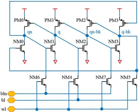
Fig.1 Circuit schematic of DICE SRAM cell
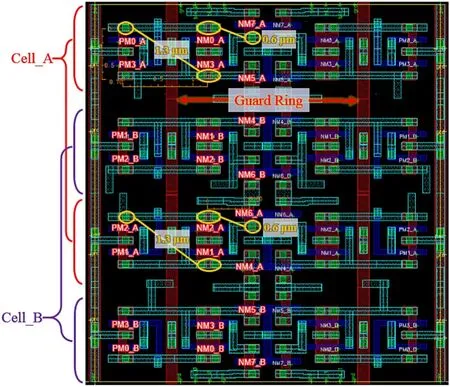
Fig.2 (Color online)Layout schematic of 65 nm dual DICE interleaving SRAM involving four DICE cells
Heavy ion irradiation experiments were performed at the Heavy Ion Research Facility in Lanzhou(HIRFL)at the Institute of Modern Physics,Chinese Academy of Sciences,and at the HI-13 Tandem Accelerator at the China Institute of Atomic Energy.At the HI-13 Tandem Accelerator,the irradiation tests of C and Si ions were conducted in a vacuum chamber.The flux of C and Si ions was controlled at 104ions/(cm2?s),and the fluence of each test exceeded 106ions/cm2.At the HIRFL,the DUT was placed on an air platform and irradiated by Kr and Ta ions,separately.The flux at the HIRFL was approximately 103ions/(cm2?s),and the fluence of each test exceeded 2×10⁵ions/cm2.Both the air layer and aluminum foil were utilized as energy degraders to adjust the energy of the incident ions.The detailed parameters of heavy ions after they have passed through a 5μm-thick passive layer of the DUT,and the experimental conditions are shown in Table 1.
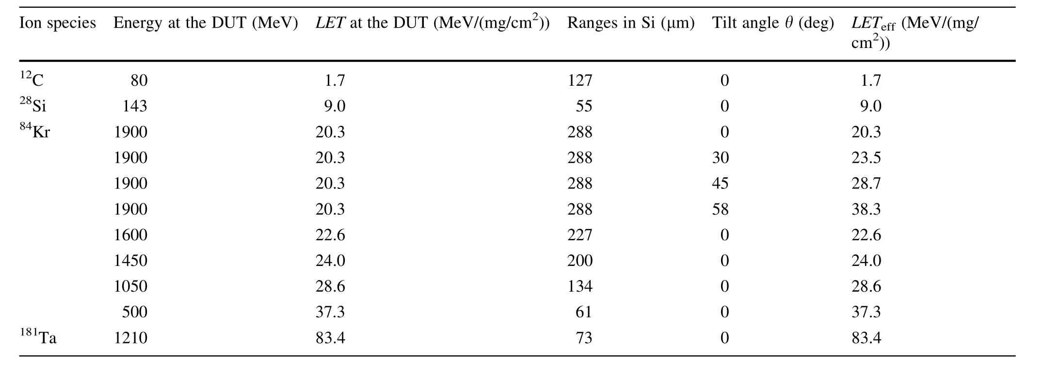
Table 1 Parameters for heavy ion irradiation tests
The DUTs used in the experiments were decapped prior to irradiation.During heavy ion tests,the DUT was placed on a field-programmable-gate array-based testing system and supplied with a core voltage of 1.2 V as well as a peripheral input/output(I/O)voltage of 3.3 V by the testing system.The EDAC code of the 1 KB block was enabled by a control program in a host computer.Different data patterns,including checkerboard data(003F),blanket zero data(0000),and blanket one data(FFFF),were employed.A data pattern was written into the DUT by the testing system prior to irradiation.To detect SEUs in real time,a dynamic readback mode was used to periodically read the stored data of the DUT during irradiation.The readback frequency was up to 1 kHz,which guaranteed the fast extraction of SEUs.By comparing the logical value of a bit in the previous readback period and the current readback period,the testing system can easily determine the occurrence of an upset.For each readback period,the testing system recorded the detected SEU information,including the error data,logical addresses of upset bits,and time stamps.After irradiation,the actual positions of the upset bits were obtained by mapping the transformation between the logical and physical addresses of the DICE cells.Subsequently,they were displayed in the form of a fault map to extract multi-bit upsets(MBUs).In addition,a Kr ion irradiation test with a tilt angleθf(wàn)rom 30°to 60°was performed,whereθis the angle between the incident direction of heavy ions and the normal direction of the DUT surface.The Kr ions in the tilt test hit the DUT surface along the horizontal direction of the layout(perpendicular to the direction of the red guard rings,as shown in Fig.2).
3 Heavy ion irradiation results and analysis
The heavy ion irradiation results are shown in Fig.3.The SEU cross sections of the 4 KB and 1 KB blocks were tested under three data patterns.The points with a downward-pointing arrow in the figures indicate that the values of the SEU cross sections are zero.The 1/error bars representing one standard deviation from the measured values are marked,whereNis the number of SEUs measured in each irradiation test.The experimental results show a significant SEU data pattern dependence in both the 4 KB and 1 KB blocks.Under the blanket zero data pattern,the DUT showed the highest SEU sensitivity.Although the SEU cross sections of the checkerboard data were less than those of the blanket zero data at all times,the SEU response of the checkerboard data exhibited a trend similar to that of the blanket zero data.However,the DUT with the blanket one data exhibited better SEU tolerance compared with the other data patterns.Under the blanket one data pattern,SEUs did not appear in the DUT until theLETincreased to 83.4 MeV/(mg/cm2),but the number of SEUs was still rare.The Weibull function,as shown in Eq.(1),was utilized to fit the SEU cross sections of the blanket zero data.
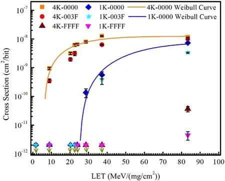
Fig.3 (Color online)SEU cross sections of 4 KB and 1 KB blocks under diverse data patterns
whereσis the SEU cross section,σsthe saturation SEU cross section,kis a dimensionless parameter known as the shape factor,dis a dimensionless parameter known as the exponential factor,andLETthis the thresholdLETfor SEU occurrence.According to the fitted curves in Fig.3,theLETthof the 4 kB and 1 kB blocks were 6 and 25 MeV/(mg/cm2), respectively. Meanwhile, their σswere 1.25×10⁻⁸and 7.7×10⁻⁹cm2/bit,respectively.Compared with the standard 6 T SRAM(LETth=0.3 MeV/(mg/cm2),σs=1.85×10–8cm2/bit)fabricated via an identical technology node as the DUT[43],both theLETthandσsof the 4 KB block were superior.The 1 KB block with the EDAC code effectively mitigated the SEUs,demonstrating a higher radiation resistance than the 4 KB block.The results reflect the effectiveness of the dual DICE interleaving design as well as the EDAC code in the 65 nm technology node.Under the blanket zero data,as theLETincreased from 28.6 to 83.4 MeV/(mg/cm2),the ratio of the 4 KB block SEU cross sections to those of the 1 KB block reduced by approximately two orders of magnitude.This reduction indicates that the effectiveness of the EDAC code diminished in the highLETvalue tests.Because the EDAC code can only correct one-bit errors in each word,the failure of the EDAC code was likely associated with the MBU in a single word.Moreover,the DUT operated stably during the entire irradiation period.No SELs occurred in the DUT owing to the design of the guard rings in the layout.The guard rings reduced the effect of minority carriers in a parasitic bipolar junction transistor and restrained the NPNP as well as PNPN structures by maintaining well potentials within an appropriate range.Hence,it can be concluded that the DUT can effectively eliminate SELs.
Physical addresses representing the actual positions of the upset bits were plotted in a fault map based on the recorded logical addresses.Figure 4 shows the bit mapping results of the upset data,which were measured in the 4 KB block at anLETvalue of 37.3 MeV/(mg/cm2)under two data patterns(no SEUs occurring under the blanket one data pattern).Each gray pixel in the fault map represents an upset bit(an upset DICE cell).The gray cross in the fault map represents the area of the peripheral circuit.In the fault map of the blanket zero data,the upset positions showed a random distribution throughout the DUT.However,the upset positions of the checkerboard data just appeared randomly in the central area.The difference in the upset position distributions was another manifestation of SEU data pattern dependence.Under the checkerboard data pattern,the logical‘‘0’’bits were concentrated in the center area of the DUT.On the contrary,all the bits located outside the center area stored the logical‘‘1’’.Hence,the SEU data pattern dependence arose from the fact that the radiation sensitivity of the logical‘‘0’’bit was much higher than that of the logical‘‘1’’bit.This may be attributable to their different sensitive area distributions.Details regarding the sensitive area distributions are provided in Sect.4.The C#-based data processing program distinguishes single-bit upsets(SBUs)and MBUs based on the spatial correlation of the physical addresses measured in each readback period.The results show that most of the SEUs were SBUs.Although the rest of SEUs were MBUs,they were all double-bit upsets.Even in the Ta ion irradiation test,no MBUs with more than two bits appeared in the DUT.
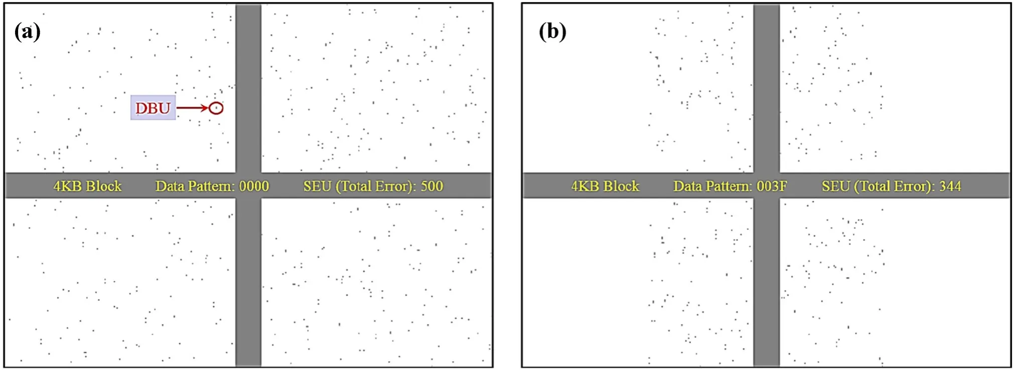
Fig.4(Color online)Mapping result of upset bits in 4 kB block at LET of 37.3 MeV/(mg/cm2)for a blanket zero data pattern and b checkerboard data pattern
The numbers of MBUs were extracted for the 4 KB block under the blanket zero data.Figure 5 shows the MBU percentage vs.theLET.As theLETincreased from 22.6 to 83.4 MeV/(mg/cm2),the MBU percentage increased monotonically from 0%to approximately 57%.The high MBU proportion of the Ta ion irradiation indicates that a significant charge sharing effect occurred in the DUT.In this case,MBUs dominated the occurrence of SEUs.The MBU cross sections of the 4 KB block and the SEU cross sections of the 1 KB block were compared,as shown in Fig.6.It was observed that the MBU cross sections were almost equal to the SEU cross sections at a certainLETvalue within an acceptable error range.The consistency of the cross sections demonstrates that the SEUs occurring in the 1 KB block were indeed caused by the MBU.The 1 KB block exhibited high SEU tolerance in lowLETvalue tests because the EDAC code effectively eliminated the SBUs.However,the MBU proportion increased with theLETvalue.The EDAC code was invalid for the MBUs because it could not correct the two-bit errors in each word.Therefore,the SEU cross sections of the 1 KB block increased with theLETvalue and gradually approached the SEU cross sections of the 4 KB block.Employing appropriate strategies at either the circuit level or layout level to mitigate MBUs in each word is essential for the effective implementation of the EDAC code.One technique that can be employed at the layout level is to insert well contacts between adjacent cells.The size and number of well contacts determine the efficacy in mitigating the charge sharing effect,while the corresponding area costs are incurred.This technique involves a tradeoff between high radiation resistance and area-saving purposes in the layout.Another option is to separate the physical addresses of cells belonging to the same word from each other.This strategy is advantageous in that the threshold of MBU occurrence within a word is improved without incurring additional area costs.For a highLETvalue irradiation,the benefit of the EDAC code can be further improved by combining these techniques.
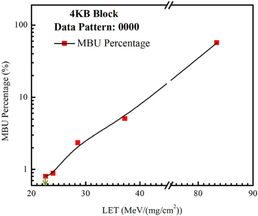
Fig.5 MBU percentage vs.LET for 4 KB block under blanket zero data pattern
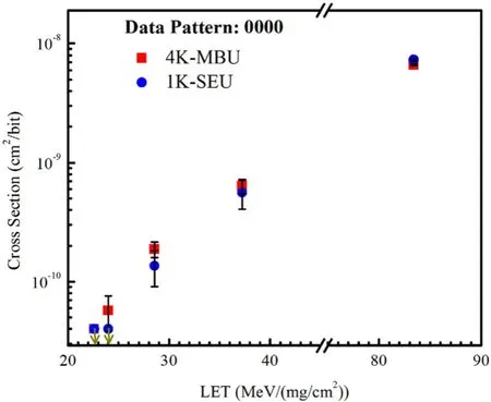
Fig.6 Comparison between MBU cross sections of 4 KB block and SEU cross sections of 1 KB block
The tilt angle irradiation test was conducted on the 4 KB block under the blanket zero data,using Kr ions with anLETvalue of 20.3 MeV/(mg/cm2).Compared with normal incident situations,the tilted incident ions traveled a longer distance in the active regions of the DUT and thus deposited more energy,which transformed into electron–hole pairs.For this reason,the effective linear energy transfer(LETeff)value should be used to denote the ionization intensity of heavy ions in Si.TheLETeffvalues of the heavy ions used in the experiment were calculated and are listed in Table 1.The results of the tilt test are shown in Fig.7.It was observed that the SEU cross sections increased with the tilt angleθ.This result is primarily due to the increase inLETeff.Moreover,the SEU cross sections of the tilt and normal tests were compared,as shown in Fig.7.It was discovered that the SEU cross sections of the tilt test were larger than those of the normal test at an approximateLETeffvalue.The difference between the tilt and normal tests became more evident asθincreased.This phenomenon may be attributable to the fact that the sensitive node pairs of the cell were more susceptible to the tilted incident ions,owing to the lateral movement of heavy ions in the DUT.The lateral traveling distance increased withθ,which increased the probability of two nodes belonging to a sensitive node pair being simultaneously affected by a heavy ion.Consequently,the SEU hardening effectiveness of the DICE structure decreased asθ increased.
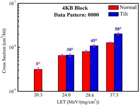
Fig.7 (Color online)Comparison of SEU cross sections between tilt and normal tests
4 HSPICE simulation and discussion
In this section,the SEU sensitivity of single storage nodes and storage node pairs of the DICE cell was investigated via circuit-level HSPICE simulation.Sensitive area distributions under different logical values were analyzed.The SEU data pattern dependence was revealed based on the sensitive area distributions.Moreover,the impacts of process,voltage,and temperature(PVT)variations on the SEU sensitivity were investigated by simulation.Based on the analysis results,some suggestions are provided to further improve the SEU tolerance of the dual DICE interleaving design.
Based on the 65 nm bulk CMOS technology library supplied by foundry,HSPICE simulation was conducted to investigate the radiation response of the cell.The transient pulse injection of the HSPICE simulation was generated using a classical double exponential pulse current source model[44],and the associated equation is as follows:
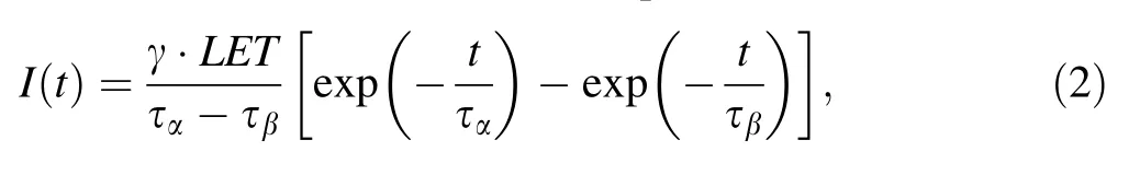
whereγis a constant related to the collection depth of the sensitive volume,ταis the junction collection time constant,andτβis the ion-track establishment time constant.The physical meaning of‘‘γ?LET’’in the equation is the amount of charge deposited by a heavy ion.In all simulations,ταandτβwere set to 200 and 50 ps,respectively[45].The value ofγwas determined using the experimentalLETthof the standard 6 T SRAMfabricated by the identical technology as the DUT.Whenγwas 0.041 pC?mg/(MeV?cm2),the simulationLETthof the 6 T SRAM cell was consistent with the experimentalLETth.Pulse current sources were added to the circuit nodes to simulate a single event of a heavy ion hitting the DUT.In the simulations without special statement,the process corner was set to‘‘TT’’,the temperature to 25°C,and the core voltage to 1.2 V.
A pulse injection simulation of single nodes was performed to verify the single node robustness of the cell.The single-node simulation involved only two cases.Whether the logical value of the cell is‘‘0’’(qn,q,qn-bk,q-bk=1,0,1,0)or‘‘1’’(qn,q,qn-bk,q-bk=0,1,0,1),a storage node is either at voltage level 0 or voltage level 1.The four storage nodes of the cell have no difference in the singlenode simulation owing to the symmetry of the DICE structure.Therefore,the simulation was simplified as follows:The initial state of the cell was set to the logical‘‘0’’,and then,a transient pulse was injected to node q(voltage level=0)and node qn(voltage level=1)at simulation times of 2 and 8 ns,respectively.The simulation results are presented in Fig.8.
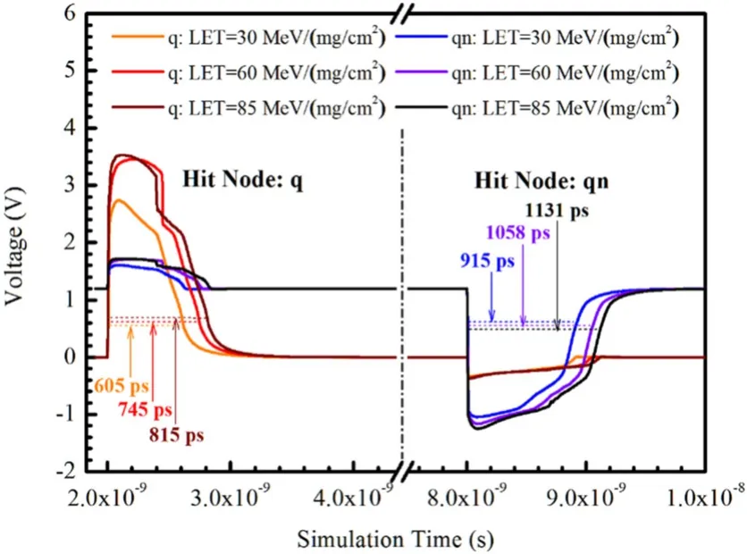
Fig.8 Simulation result of single storage node.(Color figure online)
The results show that the voltage amplitudes of the hit nodes increased with theLETvalue of the injected pulse.Taking 0.6 V(one-half of the core voltage)as reference value for the voltage level conversion,the recovery time of the voltage disturbance is marked in Fig.8.Although the voltage of a hit node completed a conversion from 0 to 1(node q)or 1 to 0(node qn)during the transient of pulse injection,the disturbed voltage returned to the initial state after hundreds of picoseconds.Even if theLETvalue of the pulse is up to 85 MeV/(mg/cm2),the hit nodes were still restored to the initial state as the transient is over.It was found that the recovery time increased with theLETvalue.This is because the collected charge of the node is proportional to theLETvalue.The collected charge was swept away by the drive current of the on-state transistors,and the sweeping time increased with the amount of collected charge.Additionally,the recovery time of node qn was longer than that of node q.This is due to the drive current of the NMOS transistor larger than that of the PMOS transistor.Under the logical‘‘0’’,the collected charge of node q was swept away by NM1,whereas that of node qn was swept away by PM0,resulting in a longer recovery time by node qn.The simulation verified the superior SEU resistance of the single nodes.The heavy ions could not induce an upset in the cell by disrupting a single node.
The simulation of node pairs is more complex.Under each logical value,the four storage nodes have six pairing ways.In other words,the node pair simulation involved twelve node pairs.According to the voltage level of two nodes belonging to a node pair as well as their relative positions in the circuit,the twelve node pairs were classified into four cases,as shown in Table 2.The node pairs belonging to the same case were equivalent at the circuit level.Only one node pair in each case required to be simulated.(In Table 2,the node pairs marked in bold font were simulated.)The initial state of the cell was set to the logical‘‘0’’.Two identical pulses were injected into the two nodes of a node pair at the simulation time of 2 ns.In particular,the simulation of node pairs considered the fact that charges deposited by a heavy ion were simultaneously collected by two nodes.Hence,the amount of injected charge at each node was one-half the total deposited charge(0.5?γ?LET).The simulation results for the four cases are shown in Fig.9.
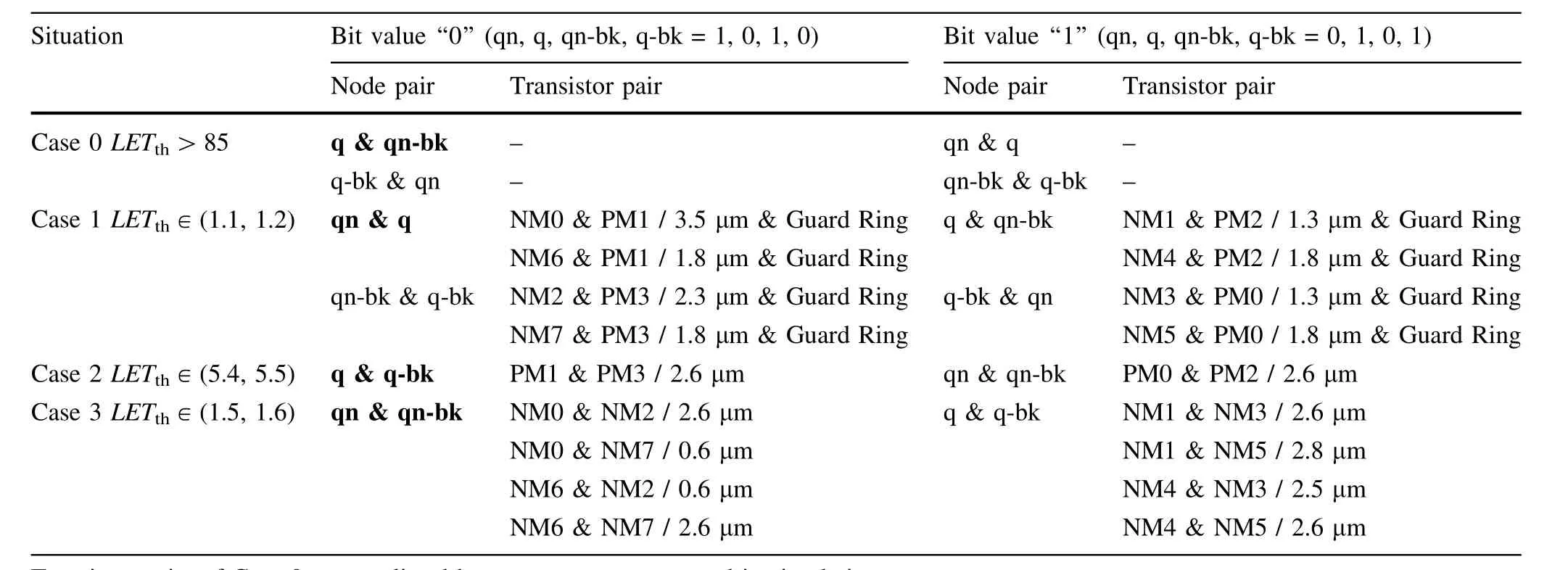
Table 2 Classification of storage node pairs and spacings of sensitive transistor pairs
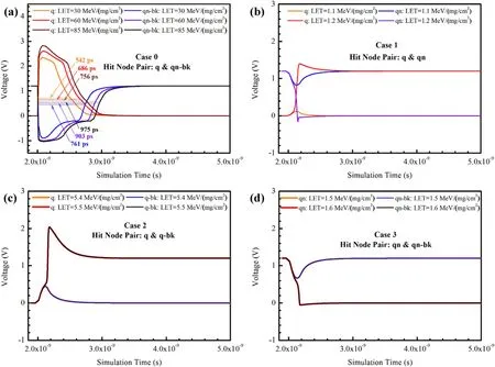
Fig.9 Simulation result of storage node pairs for a Case 0,b Case 1,c Case 2,and d Case 3.Note that in c and d,orange line coincides with blue line,and red line coincides with black line.(Color figure online)
The simulation results show that the four kinds of node pairs exhibited different SEU sensitivities.The circuit response of Case 0 was similar to that of the single nodes.No upset occurred when theLETof the injected pulse was less than 85 MeV/(mg/cm2).The recovery time of nodes q and qn-bk was consistent with the law of a single node,as discussed above.An upset was observed for each of Cases 1,2,and 3.The correspondingLETthvalues were 1.1–1.2,5.4–5.5,and 1.5–1.6 MeV/(mg/cm2),respectively.The simulation results indicate that the occurrence of SEUs was attributed to the node pairs belonging to these three cases being disrupted by a heavy ion.TheLETthmeasured in the experiment was approximately 6 MeV/(mg/cm2),which is greater than the minimum value of 1.1–1.2 MeV/(mg/cm2)obtained in the simulation.In fact,the electron–hole pairs induced by a heavy ion may be collected by multiple transistors simultaneously owing to the charge sharing effect.These transistors might not belong to the same sensitive node pair.Moreover,the deposited charge may also be collected by the well contacts as well as guard rings.Therefore,the disruption induced by a heavy ion will be dispersed,resulting in the experimentalLETthgreater than the simulationLETth.Additionally,charge collection among multiple nodes even causes the pulse quenching effect.In the DICE cell,NM0,NM3,NM5,and NM7 were adjacent to each other in the layout,and their drains were connected to nodes qn,qn-bk,and q-bk,as shown in Figs.1 and 2.This implies that nodes qn,qn-bk,and q-bk were easily disrupted by a heavy ion simultaneously.For NMOS transistors,the drain collects electrons,and thus,the voltage of the drain node is pulled down.If NM0,NM3,NM5,and NM7 are simultaneously disrupted by a heavy ion,the voltages of nodes qn,qn-bk,and q-bk will decrease accordingly.For the logical‘‘0’’(qn,q,qn-bk,q-bk=1,0,1,0),the voltage decreases of nodes qn and qn-bk tend to change the storage state.However,the voltage decrease of node q-bk not only results in an overdrive state in PM2,but also a strong off-state in NM0.The larger drive current of PM2 enables the excess charge accumulated at node qn-bk to be swept away more quickly.And the strong off-state of NM0 facilitates the recovery of node qn.The voltage decrease of node q-bk also increases its own single-event transient(SET)tolerance.This suppression effect is known as indirect LEAP SET suppression,which is a category of the pulse quenching effect[46].NM1,NM2,NM4,and NM6 are also affected by the indirect LEAP SET suppression owing to their adjacent positions.Overall,the indirect LEAP SET suppression increased the robustness of the DICE cell,resulting in a higherLETthin the experiment.
The reverse-biased drain regions of off-state NMOS and PMOS transistors in digital ICs are regarded as SEU-sensitive nodes[47],and the corresponding transistors are referred to as sensitive transistors in this analysis.When the cell stored the logical‘‘0’’,the sensitive transistors connected to nodes qn,q,qn-bk,and q-bk were NM0 with NM6,PM1,NM2 with NM7,and PM3,respectively.For the logical‘‘1’’,the sensitive transistors connected to the four nodes were PM0,NM1 with NM4,PM2,and NM3 with NM5,respectively.Subsequently,sensitive transistor pairs were obtained by pairing the sensitive transistors based on the sensitive node pairs listed in Table 2.
Taking Cell A in Fig.2 as an example,the spacings of sensitive transistor pairs in the layout(distance between the centers of the reverse-biased drain region)are listed in Table 2.The transistor pairs with minimum spacing are marked in the layout with yellow circles,as shown in Fig.2.For the logical values‘‘0’’and‘‘1’’,the minimum spacings of the transistor pairs were 0.6 and 1.3μm,respectively.Hence,the cells with the logical‘‘0’’were more sensitive to the heavy ions.Furthermore,for the logical‘‘1’’,a guard ring was inserted between the transistors of the minimum-spacing transistor pair.The guard ring improves the radiation resistance of the transistor pair owing to its ability in absorbing the deposited charge.In general,both the minimum spacing of the transistor pairs and guard rings rendered the radiation sensitivity of the logical‘‘0’’cell much higher than that of the logical‘‘1’’cell.For the blanket zero data,all cells stored the logical‘‘0’’,resulting in the highest radiation sensitivity of the DUT.However,for the blanket one data,all cells stored the logical‘1’’,resulting in the highest radiation resistance of the DUT.In other cells,the layout of the transistors was a mirror symmetry of Cell A,and the results obtained were the same as above.It is noteworthy that the minimum spacing of the sensitive transistor pairs under the logical‘‘0’’was only 0.6μm.This is caused by the insufficient isolation of the transfer transistors(NM4,…,NM7).For the logical‘‘0’’,NM0&NM7 and NM6&NM2 constituted the minimum-spacing transistor pairs,with a spacing of 0.6μm.For the logical‘‘1’’,the minimum-spacing transistor pairs were composed of fully isolated core transistors(PM0&NM3;PM2&NM1),with a larger spacing of 1.3μm.Therefore,for a layout hardening design,the effect of transfer transistors on SEU sensitivity is nonnegligible and should be examined closely.
The radiation resistance of the cell can be further improved by adjusting the layout positions of the minimum-spacing transistor pairs.A flexible solution is to swap the positions of transistors NM6 and NM7.For the logical‘‘0’’,adjustment increases the minimum spacings of the transistor pairs to 1.8μm,and the minimum-spacing transistor pairs are isolated by a guard ring.The improved radiation hardening strategy is expected to increase the radiation tolerance of the logical‘‘0’’to consistent with the logical‘‘1’’(LETthgreater than 37.3 MeV/(mg/cm2)after the adjustment).Furthermore,EDAC code can be used in the radiation hardening strategies at the circuit level to further enhance the radiation resistance.In summary,by adjusting the positions of minimum-spacing transistor pairs and separating the physical addresses of memory cells belonging to the same word,superior SEU robustness can be achieved at the layout level and circuit level,respectively.
The impacts of the PVT variations on the SEU sensitivity were investigated via simulation.The simulation results for Cases 1,2,and 3 are shown in Fig.10.Using the process corner‘‘TT’’,room temperature 25°C,and standard core voltage 1.2 V as reference value,the maximum floating percentage ofLETthis marked in Fig.10.The results show that theLETthof Cases 1,2,and 3 exhibited the same variation trend.In the simulation result of the process corner,theLETthof process corner‘‘SS’’was lower because the transistors at that process corner had a smaller drive current,causing the DICE cell to be more vulnerable to SEUs.By contrast,the transistor drive current of process corner‘‘FF’’was larger,so the cell possessed a higherLETth.For the impact of the process corner,theLETthof Case 1 exhibited the most significant fluctuation,ranging from-26.1 to+26.1%.Meanwhile,the simulation results indicate that theLETthincreased with the core voltage.This is because a larger voltage causes a higher SEU critical charge and a larger transistor drive current.For the impact of the core voltage,theLETthof Case 1 exhibited the most significant fluctuation,ranging from-43.5 to+43.5%.This suggests that the core voltage has a strong modulation to the SEU sensitivity.Additionally,the simulation results show that theLETthdecreased with increasing temperature,which is associated with the temperature dependence of the carrier mobility and threshold voltage[48].For the impact of the ambient temperature,theLETthof Case 2 exhibited the most significant fluctuation,ranging from -11.0 to+18.3%.Compared with the core voltage and process corner,the ambient temperature modulated the SEU sensitivity weakly within the simulation range.These results clearly indicate that the SEU sensitivity of the DICE cell may fluctuate significantly with variations in the PVT.Hence,designers must reserve extra margins for electronic systems operating in extreme environments.
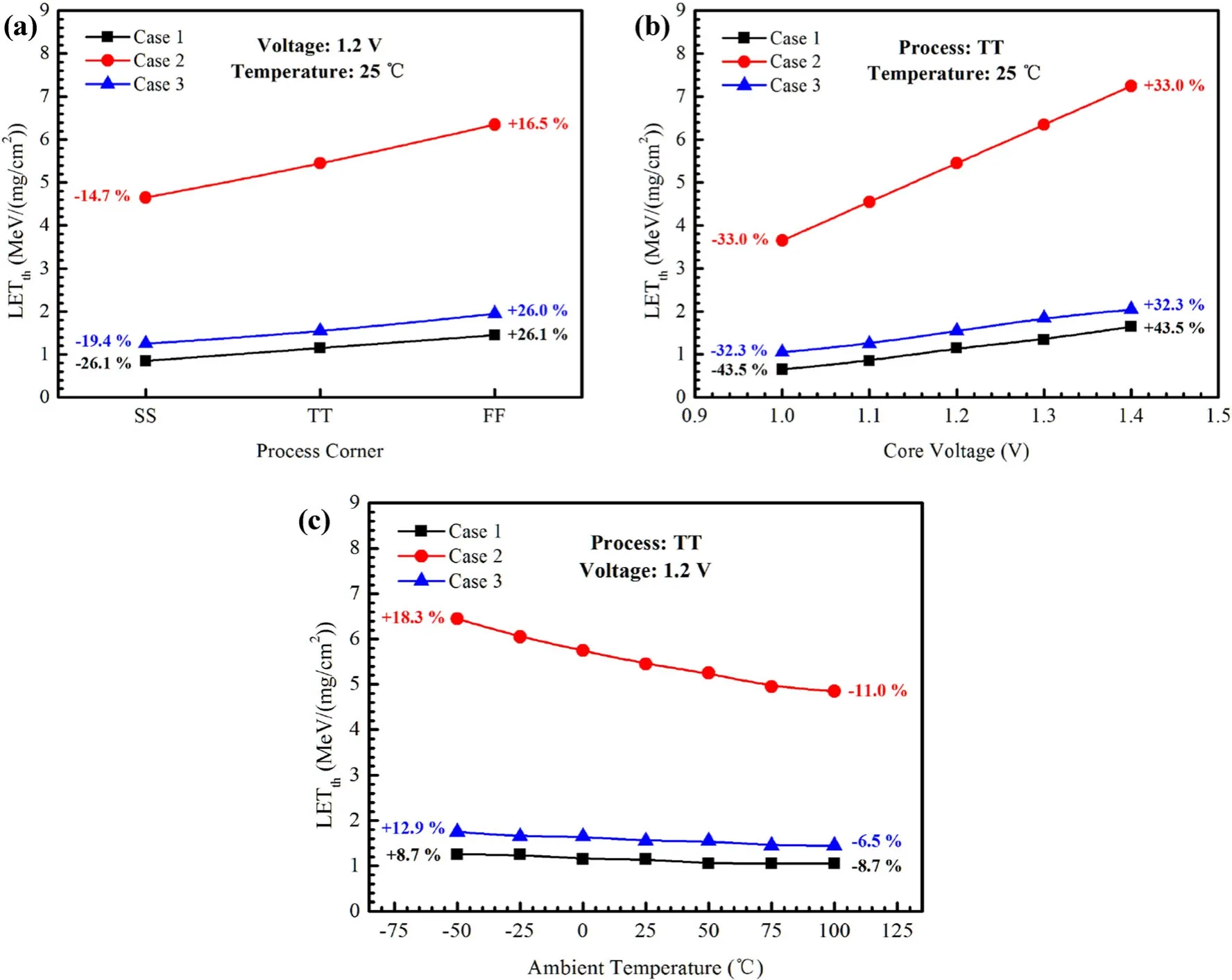
Fig.10 (Color online)Simulation results of LET th vs.a process corner,b core voltage,and c ambient temperature
The heavy ion experimental results of a conventional DICE SRAM fabricated using the identical technology as the DUT have been reported[41].A comparison of the experimental results between the designed dual DICE interleaving SRAM and the conventional DICE SRAM is shown in Fig.11.For the dual DICE interleaving SRAM,Fig.11 shows only the results of the blanket zero data pattern(the most vulnerable to SEUs)and blanket one data pattern(the most robust to SEUs).TheLETthandσsunder different conditions are listed in Table 3.It was observed that the dual DICE interleaving SRAM demonstrated higher SEU robustness.Under the blanket zero data pattern,theLETthof the 4 KB and 1 KB blocks was twice and eight times that of the conventional DICE SRAM,respectively.This suggests the efficiency of the dual DICE interleaving design and EDAC code in improving the SEU resistance.Furthermore,under the blanket one data pattern,theLETthof the 4 KB and 1 KB blocks exceeded 37.3 MeV/(mg/cm2),which indicates that theLETthof the developed SRAM will be ten times higher than that of the conventional DICE SRAM after swapping the positions of NM6 and NM7.The dual DICE interleaving design achieved superior SEU resistance with negligible power consumption and area cost compared with the conventional DICE cells,indicating its broad application prospects in the field of aerospace.Based on the experimental results and analyses presented herein,designers can employ the appropriate strategies to implement an SEU tolerance chip for diverse heavy ion radiation environments.

Table 3 LET th andσs of dual DICE interleaving SRAM and conventional DICE SRAM
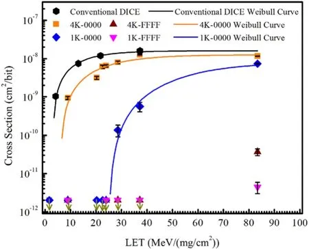
Fig.11 (Color online)Comparison of heavy ion experimental results between dual DICE interleaving SRAM and conventional DICE SRAM
5 Conclusion
In this study,the radiation response of 65 nm dual DICE interleaving SRAM was characterized via a series of heavy ion irradiation tests.The SEU cross sections and upset fault maps of the DUT under diverse data patterns are presented.The experimental results showed that both theLETthandσsof the DUT were superior to those of the standard 6 T SRAM and the conventional DICE SRAM.TheLETthof the DUT was improved significantly when the EDAC verification code was used.However,for heavy ion irradiation tests with a highLETvalue,the benefit of the EDAC code was reduced or even invalid.Therefore,the MBU resistance of devices must be enhanced while minimizing area costs.In the tilt test,the phenomenon where the SEU cross sections increased with the tilt angle was primarily due to the increase inLETeff.And the SEU cross sections also increased with the probability of sensitive node pairs being disrupted by heavy ions.Furthermore,the SEU data pattern dependence of the SRAM was primarily attributed to the specific features of the sensitive area distribution under diverse data patterns.The sensitive node pairs of the DICE cell were determined via HSPICE simulation.The spacings of sensitive transistor pairs were obtained based on the layout.By adjusting the positions of minimum-spacing transistor pairs,theLETthof an SEU occurring in the SRAM is expected to increase to more than 37.3 MeV/(mg/cm2)for all data patterns.Because the radiation resistance of the SRAM enhanced significantly,while a relatively small area and low electrical performance costs were maintained,the designed SRAM is extremely suitable for applications used in harsh radiation environments.The irradiation results presented herein will promote the application of dual DICE interleaving and EDAC code strategies in advanced nanoscale technology nodes,provide guidance to designers,and furnish sufficient SEU data for on-orbit applications.
AcknowledgementsThe authors would like to thank the members of the Heavy Ion Research Facility in Lanzhou(HIRFL)and HI-13 Tandem Accelerator for their support during the testing conducted.
Author contributionsAll authors contributed to the study conception and design.Material preparation,data collection and analysis were performed by Tian-Qi Liu,Ze He and Shi-Wei Zhao.The first draft of the manuscript was written by Ze He,and all authors commented on previous versions of the manuscript.All authors read and approved the final manuscript.
 Nuclear Science and Techniques2021年12期
- Nuclear Science and Techniques的其它文章
- Fast nuclide identification based on a sequential Bayesian method
- Screener3D:a gaseous time projection chamber for ultra-low radioactive material screening
- Performance evaluation of ultra-long lithium heat pipe using an improved lumped parameter model
- Absorption effect of pure nickel on the corrosion behaviors of the GH3535 alloy in tellurium vapor
- Design and development of the beamline for a proton therapy system
- Ensuring the possibility of using thorium as a fuel in a pressurized water reactor(PWR)