
Design and investigation of novel ultra-high-voltage junction field-effect transistor embedded with NPN*
2021-07-30 07:43:08XiKunFeng馮希昆XiaoFengGu顧曉峰QinLingMa馬琴玲YanNiYang楊燕妮andHaiLianLiang梁海蓮
Chinese Physics B 2021年7期
關(guān)鍵詞:梁海
Xi-Kun Feng(馮希昆), Xiao-Feng Gu(顧曉峰), Qin-Ling Ma(馬琴玲),Yan-Ni Yang(楊燕妮), and Hai-Lian Liang(梁海蓮)
Engineering Research Center of Internet of Things Technology Applications(Ministry of Education),Department of Electronic Engineering,Jiangnan University,Wuxi 214122,China
Keywords: junction field-effect transistors,NPN,electrostatic discharge(ESD)robustness,ESD protection
1. Introduction
With the rapid development of integrated technology,ultra-high-voltage (UHV) power devices are commonly used as main drive devices in power management, motors, automotive electronics,and industrial control applications.[1-3]In particular, junction field-effect transistors (JFETs) have been widely used in silicon-based high voltage integrated circuits(ICs)because of their high input impedance,low noise,small power consumption,good process compatibility,and temperature performance.[4-7]Various techniques and methods such as the long field plate,N-type drift and design of the reversed PN junction location, have been used to increase the breakdown voltage of the conventional JFETs.
In addition, the electrical performance optimization and electrostatic discharge (ESD) characteristics improvement of JFETs are simultaneously becoming an important research field with the wide applications in high-voltage ICs, because the ESD protection is developing into a severe and challenging issue in UHV JFETs. Nidhi and Ker used the P-type ESD implantation to adjust the pinch-off voltage of a novel horizontal n-channel JFET device,making JFET suitable for multi-power supplying circuit.[8]Vincentet al.explored an optimized vertical JFET,by embedding diffusion gates to harvest the excellent voltage control sensitivity and the enhanced overvoltage protection capability.[9]Nget al.proposed a novel sub-20-V planar power MOSFET device by using the ion implantation technology to reduce the on-resistance and the threshold voltage variation.[10]The above optimizations effectively improved the electrical performance of traditional JFET. However,these JFETs remain vulnerable in the human body model(HBM) test. Other solutions such as the reported JFET with an embedded silicon-controlled rectifier (SCR)[11]have been proposed to elevate the ESD robustness, which increases up from 1.93 kV to 2.63 kV. However, the ESD protection capability is still not strong enough for the increasingly harsh circuit operating environment.
The UHV JFET embedded with NPN to enhance the ESD performance is designed and investigated. By inserting the NPN structure,the JFET embedded with NPN exhibits a small voltage snapback and strong ESD robustness of 5.5 kV,which satisfies the ESD protection requirements of UHV JFETs in some special operations.
2. Device structures and operation mechanism
A similar top-view layout of three JFETs is shown in Fig.1. The corresponding cross-sections along A-A′and BB′directions of the conventional JFET are shown in Figs.2(a)and 2(b), respectively. The conventional JFET and JFETLNPN have identical structures along the A-A′direction as shown in Figs. 2(a) and 3(a). However, unlike the conventional JFET,the JFET-LNPN has a lateral parasitic NPN along the B-B′direction. The lateral NPN marked as T1 in Fig.3(a)improves the ESD robustness and turn-on speed under electrical stress.
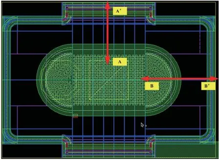
Fig.1. Similar top view of the general layout of three JFETs.
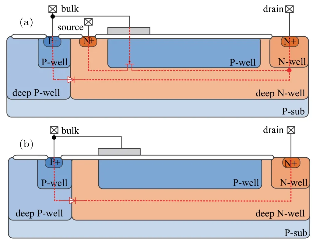
Fig. 2. (a) Cross-section along A-A′ direction and (b) cross section along B-B′ direction of conventional JFET device.
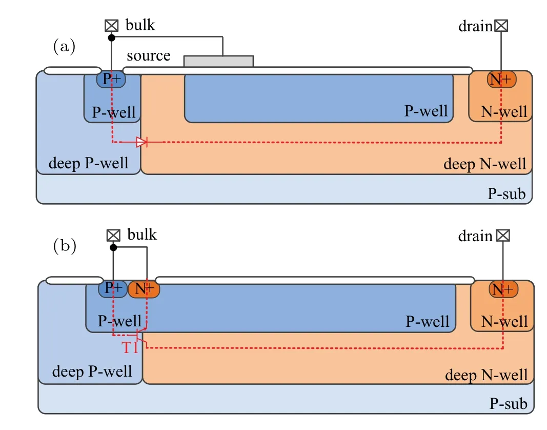
Fig. 3. (a) Cross-section along A-A′ direction, and (b) cross section along the B-B′ direction of JFET-LNPN device.
By maintaining the same structure with the conventional JFET along the A-A′direction,extending the P-well to the left deep P-well in the JFET along the B-B′direction,and inserting a high implanted N-type (N+) region into the P-well, we obtain a new JFET embedded with lateral NPN(JFET-LNPN).The cross-section of JFET-LNPN along the B-B′direction is shown in Fig.3(b).
Furthermore, by introducing an N+ region and an Nwell into the left deep P-well in the JFET-LNPN along the A-A′direction, and maintaining the structure of the JFETLNPN along the B-B′direction unchanged,we obtain an optimized JFET embedded with lateral and vertical NPNs(JFETLVNPN)as shown in Fig.4.
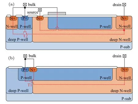
Fig. 4. (a) Cross-section along A-A′ direction, and (b) cross section along B-B′ direction of JFET-LVNPN device.
The breakdown voltage decreases because of the different reverse PN junctions. Compared with that of the conventional JFET,the reverse PN junction of the JFET-LNPN forms at the interface between the deep N-well and the top P-well. The location and doping concentration of the top P-well are valuable for optimizing the electrical performance of the JFET-LNPN.
In addition to the same lateral NPN in the JFET-LNPN and JFET-LVNPN along the B-B′direction,the JFET-LVNPN has an additional vertical parasitic NPN marked as T2 in Fig. 4(a), which dwells in the structure along the A-A′direction and helps to enhance the ESD robustness. Meanwhile,the vertical NPN is beneficial to the decreasing of the trigger voltage and the increasing of the turn-on speed due to the deep P-well parasitic resistance.
In operation,the conventional JFET and optimized JFETs embedded with the different NPNs have their own ultra-high turn-on voltage, because of the large deep N-well resistance,long field plate and top P-well. Moreover, the fabrication process of these devices is compatible with the commercial CMOS or bipolar-CMOS-DMOS (BCD) process of siliconbased ICs without extra mask cost.
3. Experimental results and discussion
3.1. Device test
The aforementioned three types of JFET devices with a width of 250 μm are fabricated in a 0.25-μm BCD process.The main process parameters of the devices are shown in Table 1. The high voltage BCD process characterized by Table 1 helps to increase the turn-on voltages of the JFETs.
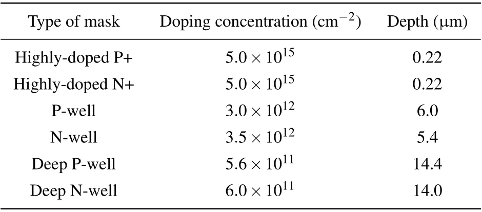
Table 1. Main process parameters of devices.
The DC electrical performances at different temperatures of the three JFETs are measured by the semiconductor tracer and variable temperature probe system. The DC test results show that the saturated voltages of the devices are all approximately 98 V, the JFETs work in the constant-current region,and the turn-on voltages of these devices are about 780 V at room temperature, which satisfies the operation requirements of the UHV JFET. When the temperature is increased to 150°C,the turn-on voltage of the JFETs slightly decreases from 780 V to 720 V;thus,the JFETs remain in a better UHV turn-on state,and exhibit good temperature characteristics.
The transient electrical performances of the JFET devices are evaluated by transmission line pulse(TLP)tests. The TLP characteristics are measured with the source end of JFETs floating and grounded. When the source end is floating, the gate and the substrate are both connected to the ground, and the drain end is stressed by a positive ESD pulse. When the source end is grounded, the source, gate and substrate are all connected together, and the drain end remains stressed by a positive ESD pulse.
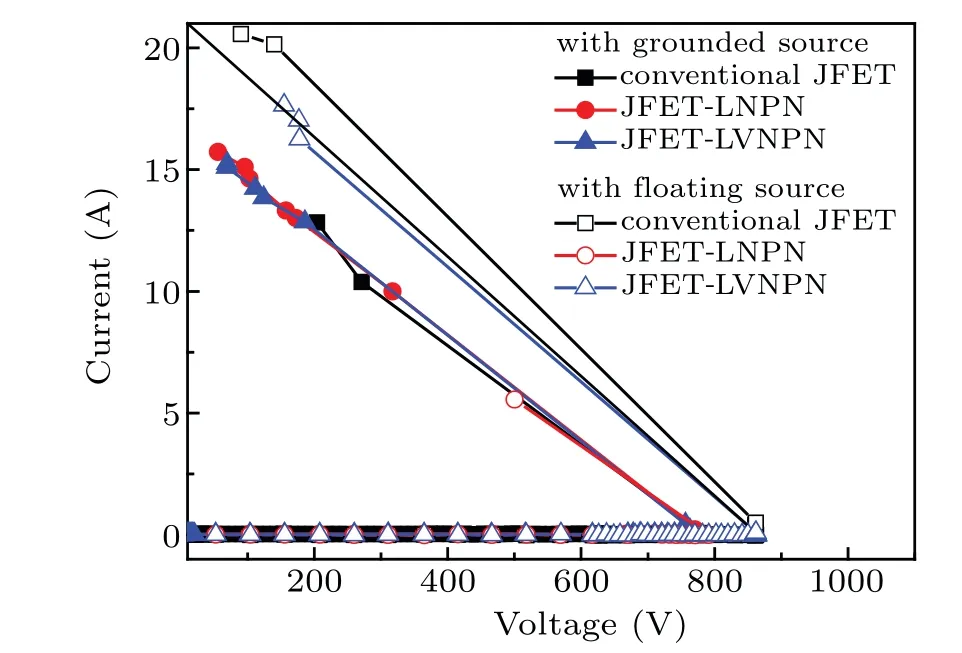
Fig.5. TLP characteristic curves of JFET devices with grounded source and with floating source.
The TLP characteristic curves are shown in Fig. 5. The curves with solid and open symbols represent the TLP characteristics of different devices with the floating and grounded source ends, respectively. The results indicate that the JFETLNPN and JFET-LVNPN have stronger ESD robustness than the conventional JFET.In addition,the holding voltages of the two optimized devices after the snapback are larger than the saturation voltage without the risk of latch-up.
The trigger voltages of the JFET devices with the floating source end and grounded source end are summarized in Table 2. The trigger voltage of the experimental device with the floating source end changes slightly,which is similar to that of the device with the grounded source end. However,compared with that of the device with the grounded source end,the trigger voltage of the conventional JFET device decreases from 861 V to 779 V because of the assistant trigger effect by the large well parasitic resistance. Meanwhile,the trigger voltage of the JFET-LNPN device decreases from 791 V to 770 V because of the combination effect of the even larger well parasitic resistance and the embedded lateral NPN in the JFET device.Similarly, the trigger voltage of the JFET-LVNPN decreases from 862 V to 756 V because of the combination effect of the lateral and vertical NPN embedded in the JFET.
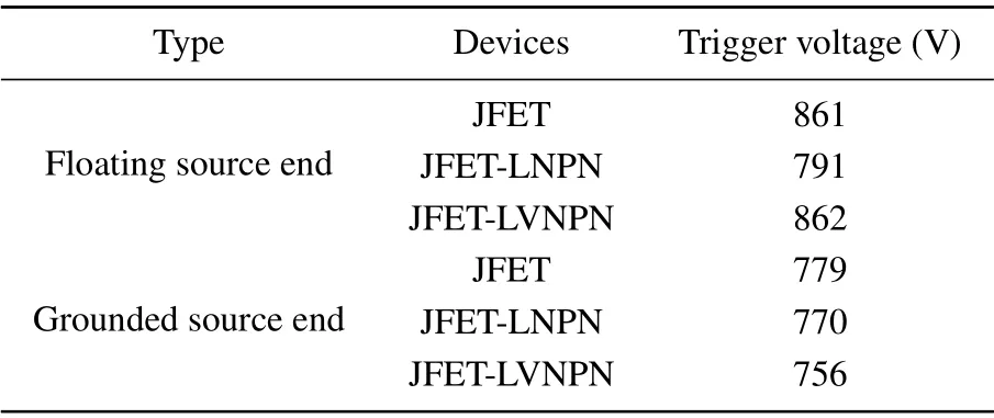
Table 2. Trigger voltages of three devices.
The ESD robustness of the JFET device is tested by the wafer ESD testing system HED-W5000M.By setting the initial ESD pulse voltage of 500 V and the step of 500 V,the ESD robustness of the conventional JFET device is 1.5 kV,which is lower than that of the 2-kV HBM ESD commercial test standard, whereas both JFET-LNPN and JFET-LVNPN can pass the 5.5-kV HBM ESD test. The tested data indicate that the ESD robustness of JFET-LNPN and JFET-LVNPN increase approximately 3.75 times due to the embedded NPN in the JFETs.
The proposed JFET simultaneously exhibits stronger ESD robustness than the 800-V SCR-JFET.[11]The main ESD characteristics of experimental devices and the 800-V SCRJFET are shown in Table 3. The trigger voltages of the JFETLNPN and JFET-LVNPN are lower than that of the 800-V SCR-JFET, which helps to improve the turn-on speed of the proposed JFETs under the ESD pulse.

Table 3. Main ESD characteristics of experimental devices and 800-V SCR-JFET devices.
3.2. Failure analysis of devices
The voltage endurance capability and inner physical mechanism of producing the damage in the JFET device are investigated by using the semiconductor tracer,scanning electron microscopy(SEM),and emission microscopy(EMMI).
When the devices are stressed by an increasing DC bias,the leakage current hardly changes. Then, the leakage current significantly increases when the DC voltage is larger than 780 V. Finally, the conventional JFET breaks down under the continuous increasing DC stress. However,the JFETLNPN and JFET-LVNPN remain robust when the DC voltage is smaller than 900 V. The delayer images obtained by SEM when the JFET devices are under the same DC stress of 780 V are shown in Fig.6.
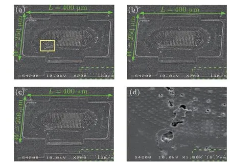
Fig. 6. Delayer images of (a) conventional JFET, (b) JFET-LNPN, and (c)JFET-LVNPN,and(d)amplified image of conventional JFET in yellow box shown in panel(a).
Compared with those of the JFET-LNPN and JFETLVNPN,the delayer image of the conventional JFET presents a damaged region as indicated by the yellow box in Fig.6(a).The amplified delayer image in Fig.6(d)demonstrates that the substrate of the conventional JFET is burned because of the thermal breakdown. Meanwhile, the good delayer images of the JFET-LNPN and JFET-LVNPN as shown in Figs.6(b)and 6(c)prove that the embedded NPN are helpful in quickly discharging the large current and avoiding the local thermal damage,without affecting the voltage endurance capability of the UHV JFET.
When the JFET-LNPN and JFET-LVNPN are stressed by continuously increasing TLP pulse, the leakage current changes on a nanoamp scale in a period of time;then,a jumping growth suddenly appears under a 900-V DC bias caused by the TLP test system. At this moment, the corresponding ESD robustness of the JFET embedded with NPN is equal to the HBM of 6 kV.
Meanwhile,the internal degradations of the JFET-LNPN and JFET-LVNPN are observed and measured by EMMI.The filament-like failure spots appear near the drain end in the JFET-LNPN,but they appear near the source end in the JFETLVNPN, which are marked by yellow arrows. Different failure positions of the JFET-LNPN and JFET-LVNPN,caused by different internal physical mechanisms,are also explored and analyzed by TCAD simulations.

Fig.7. EMMI photographs of the experimental devices((a)JFET-LNPN and(b)JFET-LVNPN)under the same DC stress.
3.3. Verification by simulations
The transient electrical performance of the JFET-LNPN and JFET-LVNPN are simulated by using the Sentaurus software. The structure simulations of JFET-LNPN and JFETLVNPN correspond to the production process, and suitable physical model and computational methods are selected to confirm the good reliability of simulating results by comparing with the measured results.
When JFET-LNPN and JFET-LVNPN with the floating source end are stressed by a pulse with a period of 100 ns and rise time of 10 ns, the electrical characteristic curves of the devices are obtained as shown in Fig.8, showing that the trigger voltages of the JFETs embedded with NPN are 889 V and 803 V. Meanwhile, the snapback voltages of the devices are 413 eV and 115 V, which are both larger than the saturated voltage of 98 V, thus, the JFETs effectively avoid the latch-up risk. So, the simulated electrical characteristics are consistent with the measured results, which confirm that the simulations are reliable. It can also be found that the JFETLVNPN has a smaller snapback voltage than the JFET-LNPN because the vertical NPN has a larger current gain than the lateral NPN. Furthermore, the large current gain of the vertical NPN in the JFET-LVNPN helps to form the parasitic SCR current discharge path, which beneficially improves the ESD robustness.
The simulated internal current density distributions of the JFETs with different structures along the A-A′and B-B′directions are shown in Fig. 9. The JFET-LNPN and JFETLVNPN have identical structures along the B-B′direction as shown in Figs.3(b)and 4(b). The internal current density distribution in Fig. 9(a) confirms that the current continues to concentrate in the drain region because of the short distance between the drain and the lateral NPN in addition to the reversed PN junction at the interface between the deep N-well and the deep P-well.
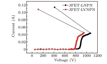
Fig.8. Simulated electrical characteristics of JFETs embedded with NPN.
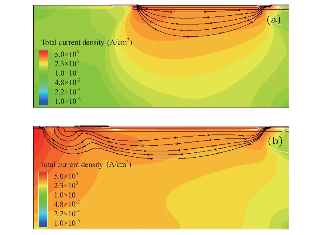
Fig.9. Internal current distributions of the JFETs with structure of(a)JFETLNPN and JFET-LVNPN along the B-B′ direction, and (b) JFET-LVNPN along the A-A′ direction.
However,figure 9(b)shows that the internal current density distribution of the JFET-LVNPN along the A-A′direction is more concentrated in the source region than that of the JFET-LNPN, indicating that two or more current conduction paths are formed in the device. Beside the lateral and vertical NPN current conduction paths, one additional parasitic SCR current conduction path is significantly helpful to increase the discharge current capacity, which enhances the ability of the N-well in the deep P-well to collect electrons. The internal current distributions of the JFETs embedded with NPN are consistent with the aforementioned analyses.
4. Conclusions and perspectives
The novel UHV JFET-LNPN and JFET-LVNPN with enhanced ESD robustness are designed and investigated by different types of test instruments and simulation tools. The TLP test results show that the ESD robustness of UHV JFETs-LVNPN increases by approximately 3.75 times, and the failure analysis performed by SEM and EMMI shows that the novel JFETs embedded with NPN have identical voltage endurance to the conventional JFETs. Moreover, the internal physical mechanism of the JFETs embedded with NPN confirms that the lateral NPN and vertical NPN are significantly useful for improving the ESD robustness. In addition,the vertical NPN has a stronger electron collecting capacity than the lateral NPN. Thus, the JFET-LVNPN is more useful for the UHV device and for the ESD protection device.
Acknowledgments
The authors would like to thank the Process Development of CSMC for providing the measured instruments and professional failure analysis tools. And this work was completed successfully under the support of many researchers worked in the CSMC.The authors are also grateful to the ESD group of Zhejiang University, Zhejiang Province, China, for providing the equipment of the transmission line pulsing system.
猜你喜歡
作文周刊·小學(xué)二年級(jí)版(2023年20期)2023-05-06 02:42:32
作文周刊·小學(xué)二年級(jí)版(2022年24期)2022-06-18 14:30:28
作文周刊·小學(xué)二年級(jí)版(2022年20期)2022-05-05 01:33:06
牡丹(2021年11期)2021-07-20 08:54:49
Chinese Physics B(2021年6期)2021-06-26 03:30:12
青年生活(2019年18期)2019-10-21 15:44:53
小學(xué)生優(yōu)秀作文(中年級(jí))(2017年9期)2017-08-09 01:31:34
作文評(píng)點(diǎn)報(bào)·低幼版(2017年9期)2017-03-23 19:17:18
西域歷史語(yǔ)言研究集刊(2015年0期)2015-08-21 08:38:46
作文評(píng)點(diǎn)報(bào)·低幼版(2015年45期)2015-05-30 10:48:04

- Chinese Physics B的其它文章
- Numerical simulations of partial elements excitation for hemispherical high-intensity focused ultrasound phased transducer*
- Magnetic-resonance image segmentation based on improved variable weight multi-resolution Markov random field in undecimated complex wavelet domain*
- Structure-based simulations complemented by conventional all-atom simulations to provide new insights into the folding dynamics of human telomeric G-quadruplex*
- Dual-wavelength ultraviolet photodetector based on vertical(Al,Ga)N nanowires and graphene*
- Phase-and spin-dependent manipulation of leakage of Majorana mode into double quantum dot*
- Deep-ultraviolet and visible dual-band photodetectors by integrating Chlorin e6 with Ga2O3