
Novel Si/SiC heterojunction lateral double-diffused metal–oxide semiconductor field-effect transistor with p-type buried layer breaking silicon limit?
2021-05-06 08:55:44BaoxingDuan段寶興XinHuang黃鑫HaitaoSong宋海濤YandongWang王彥東andYintangYang楊銀堂
Chinese Physics B 2021年4期
Baoxing Duan(段寶興), Xin Huang(黃鑫), Haitao Song(宋海濤),Yandong Wang(王彥東), and Yintang Yang(楊銀堂)
Key Laboratory of the Ministry of Education for Wide Band-Gap Semiconductor Materials and Devices,School of Microelectronics,Xidian University,Xi’an 710071,China
Keywords: Si/SiC heterojunction,LDMOS,breakdown voltage,specific on-resistance
1. Introduction
Lateral double-diffused metal–oxide semiconductor fieldeffect transistor (LDMOS) is easy to integrate with other devices and peripheral circuits. It is widely used in the smart power integrated circuits and high-voltage integrated circuits,which has attracted the attention of people in related fields.[1–5]The conventional silicon(Si)LDMOS has encountered obstacles in the application of the high power due to the mutually restrictive relationship between the specific onresistance (Ron,sp) and the breakdown voltage (BV).[6,7]Silicon carbide(SiC)material has the characteristics of the wide band gap and high BV, so it is used in the field of the highvoltage power devices.[8]However, the development of SiC power devices is limited by gate oxide because SiC has a higher density of dangling Si and C bonds at the SiC/SiO2interface.[9]The emergence of Si/SiC substrate makes it possible to solve the above problems.[10–14]
A novel Si/SiC heterojunction LDMOS with p-type buried layer (PBL Si/SiC LDMOS) is proposed in this paper for the first time. PBL Si/SiC LDMOS takes full advantages of the Si/SiC substrate by preparing the electrodes on the epitaxial layer of Si, and the drain region of the device is deep into the SiC substrate,avoiding the reliability problems of SiC gate oxide, while also taking advantage of the high critical electric field of the SiC. The drain region penetrates into the SiC substrate,that is,the breakdown point transfer(BPT)terminal technology, which modulates the vertical electric field of the device.[9,15]Meanwhile, a p-type buried layer is introduced at the Si/SiC interface to optimize the surface lateral electric field of PBL Si/SiC LDMOS.The combination of the two technologies improve the BV of the device. The structure of PBL Si/SiC LDMOS achieves a breakthrough in the limit of Si. Under the same drift region length,the novel device has higher BV and lower Rsp,oncompared to the conventional Si LDMOS and Si/SiC LDMOS with deep drain region.[16]
2. Device structure and description
The cross section of PBL Si/SiC LDMOS in Fig.1. Different from the conventional Si LDMOS,the proposed device uses p-type lightly doped SiC as the substrate,the active region of the device is prepared in the Si epitaxial layer,the drain region is deep into the SiC substrate,and a p-type buried layer is introduced at the interface between Si and SiC.SiC substrate plays three roles: first, p-doped SiC participates in depletion of n-type drift region,or the reduced surface field(RESURF)technology.[17,18]Second,it participates in modulation of vertical electric field,and deep drain region makes vertical breakdown point transfer from the edge of drain to heterojunction.Third, SiC material has high thermal conductivity, which can be used for heat dissipation of power devices. The p-type buried layer modulates the surface lateral electric field of the device to make its distribution more uniform,which increases the BV of the device.
In order to study the characteristics of PBL Si/SiC LDMOS,ISE-TCAD is used to simulate the proposed device,and the proposed device is compared with the conventional Si LDMOS and Si/SiC LDMOS with deep drain region. In this simulation,the p-type SiC substrate potential is always zero voltage. When the forward conduction characteristic is simulated,the positive gate voltage is applied to make the channel open;The gate voltage is zero when the breakdown characteristics are simulated. The standard of reverse breakdown of the device is that the drain current density exceeds 1×10?7A/μm,and the 4H–SiC parameters are used for the sic material.The physical models used in this simulation include mobility(DopingDep HighFieldsat Enormal), effective intrinsic density(OldSlotboom),and recombination(Shockley–Read–Hall(DopingDep) auger avalanche (Eparal)). The important parameters of the three devices are shown in Table 1.
The key processes of fabricating PBL Si/SiC LDMOS are presented in Fig.2. The p-type buried layer is located inside the device,so the doping process of p-type buried layer should be completed before the wafer-bonding. The formation of the Si/SiC substrate can be realized by the method in Ref.[10]and the simplified wafer-bonding processes are as follows: (a)initial SiC wafer and epitaxial growth of the Si substrate,(b)ion implantation to form the drain region in the SiC substrate and form the p-type buried layer in the Si epitaxial layer,(c)wafer bonding and wafer splitting. The remaining key processes are similar to those of the conventional Si LDMOS,which can be summarized as follows: (d) ion implantation to form the pwell and N-drift, (e) ion implantation to form the other part of the drain,(f)gate oxide and field oxide growth and ion implantation to form the source.
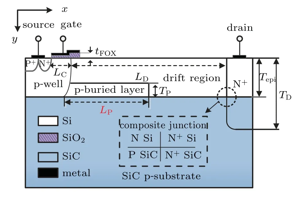
Fig.1. Cross section of PBL Si/SiC LDMOS.
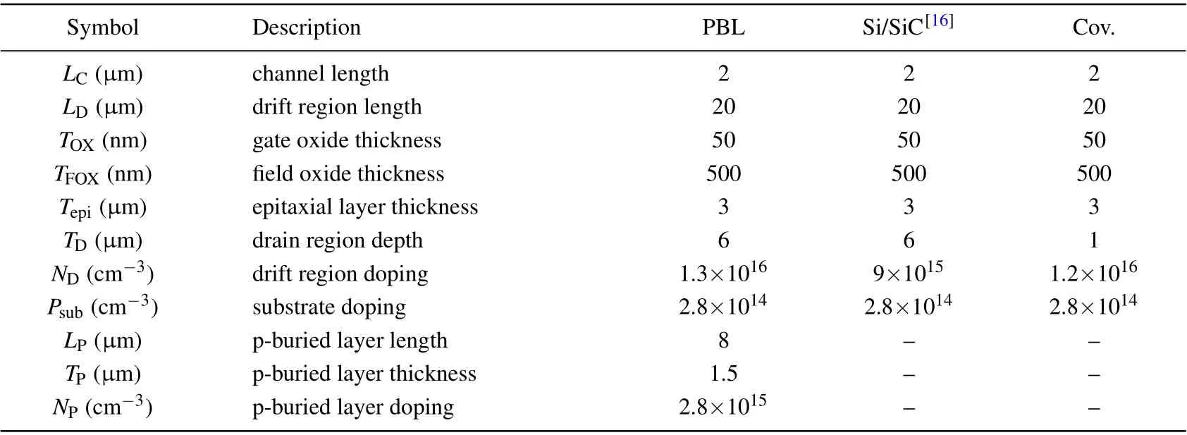
Table 1. Important parameters used in device simulation.
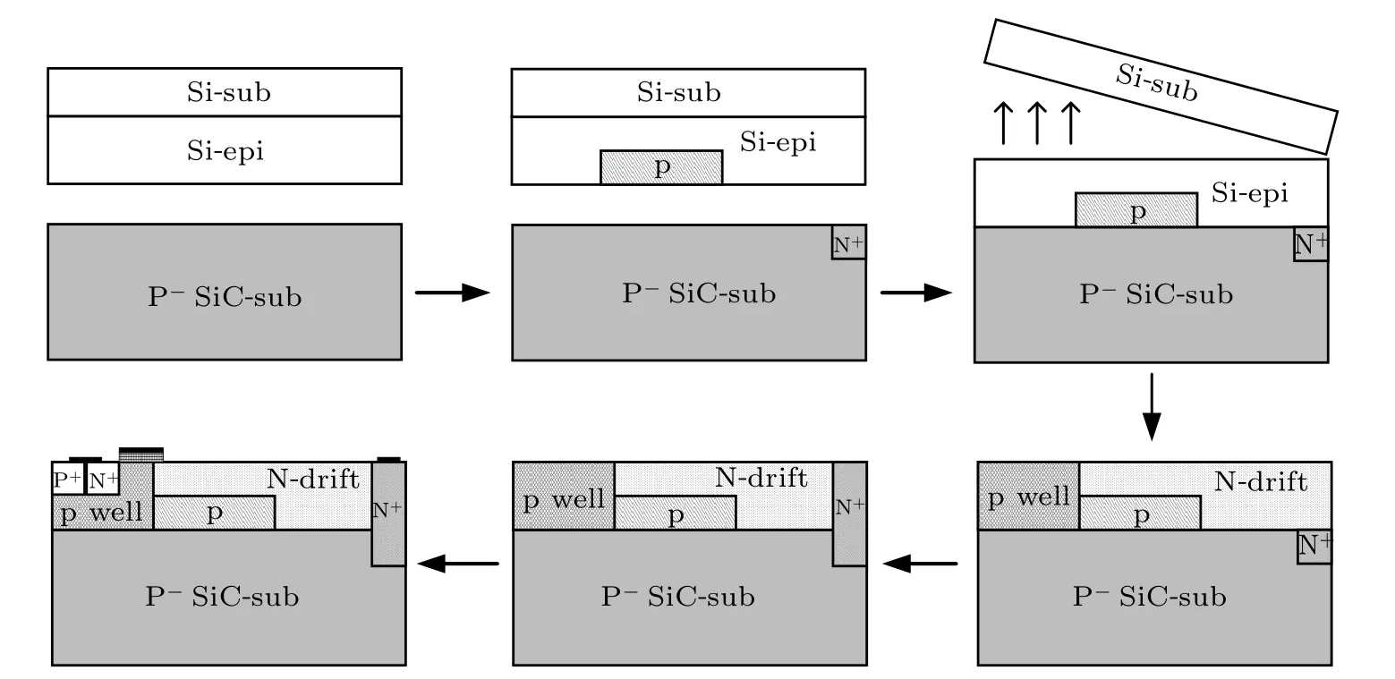
Fig.2. Simplified key processes of fabricating PBL Si/SiC LDMOS.
3. Result and discussion
In this paper,the lateral and vertical electric fields of LDMOS are optimized to improve the device performances. The proposed device introduces a p-type doped buried layer at the boundary between the drift region and the substrate, and the new buried layer will be depleted with the drift region and generate an additional electric field in the drift region. The additional electric field optimizes the surface lateral electric field of the device.[19]The drain region of the device is deep into the SiC substrate, the peak value of the vertical electric field of the device is transferred from Si to SiC. The critical electric field of SiC is larger than that of Si,thereby achieving an increase in the vertical BV.
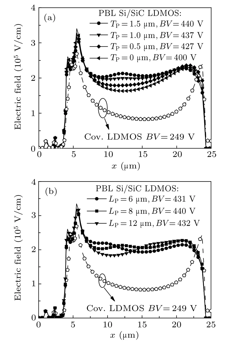
Fig.3. The influence p-type buried layer on the surface lateral electric field distribution of BPL Si/SiC LDMOS: (a) Surface electric field distributions at different TP values of the novel structure: LP=8μm. (b)Surface electric field distributions at different LP values of the novel structure: TP=1.5μm.
The effect of the size of the p-type buried layer on the lateral electric field of the device is studied. The relationship between the lateral electric field distribution of the proposed device and the p-type buried layer is shown in Fig.3.In particular,when the p-type buried layer thickness(TP)equals 0μm,the proposed device degenerates to Si/SiC LDMOS with deep drain region.Compared with the U-shaped lateral electric field of the conventional(Cov.) Si LDMOS,it is found that the ptype buried layer introduces a new electric field peak in the middle of the surface lateral electric field of the device. Figure 3(a)shows the effect of TPon the new peak in the middle of the surface lateral electric field. When TPchanges from 0.5 μm to 1.5 μm, the new peak electric field gradually increases. The peak of the electric field is caused by the PN junction formed at the interface between the right end of the p-type buried layer and the drift region. The thicker the buried layer,the stronger the peak of the electric field. When the device works in withstand voltage mode, the interface electric field of the reverse biased PN junction and the lateral electric field of Si/SiC LDMOS with deep drain region constitute the lateral electric field of PBL Si/SiC LDMOS. The BV is the integration of the electric field along the path, and the flatter lateral electric field leads to the increase of BV.
Figure 3(b)shows the relationship between the lateral position of the new peak electric field and p-type buried layer length(LP). The location of the peak of the new electric field coincides with the end position of the p-type buried layer.That is, the location of the peak of the new electric field is determined by the LP. In order to obtain a uniform lateral electric field distribution curve,the peak position of the electric field is expected to appear at the valley of the U-shaped later electric field,so the LPshould not be set too long or too short. In this simulation,when the LPis 8μm,the maximum BV can reach 440 V.
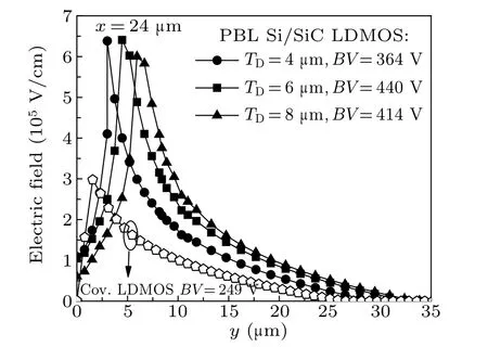
Fig.4. Vertical field distributions at different TD values of BPL Si/SiC LDMOS:LP=8μm,TP=1.5μm.
The influence of the drain region depth(TD)on the vertical electric field distribution of the proposed device has also been studied. Figure 4 shows the relationship between the vertical electric field and the TD. Compared with the conventional Si LDMOS,PBL Si/SiC LDMOS has a higher vertical peak electric field,because the bottom of the drain end of the proposed device is located on the SiC substrate with a higher critical electric field. With the increase of the TD, the position of the vertical electric field peak is farther away from the device surface(the device surface ordinate y=0). A PN junction is formed on the contact surface of the drain region and the substrate, and the vertical electric field peak is located at the interface of the PN junction. The change of the TDcauses the position of the drain liner PN junction interface to change.This is the reason why the vertical peak electric field changes with TD. The doping distribution of drain is Gaussian doping profiles, and the doping concentration decreases with the increase of diffusion depth. Therefore, with the increase of the drain region depth (TD), the doping concentration in the bottom area of the drain becomes lower, which leads to the decrease of the drain-substrate PN junction interface electric field peak. In addition, figure 4 also shows the change of the BV of the proposed device with the TDunder the given p-type buried layer parameters. When TD=6μm, the proposed device has the largest BV. When TDincreases to 8 μm, the BV of the proposed device decreases,so the drain depth should be set reasonably.
The p-type buried layer of PBL Si/SiC LDMOS will assist the depletion of the n-type drift region. When the size of the p-type buried layer changes, in order to fully deplete the n-type drift region, the concentration of the p-type buried layer and the concentration of the n-type drift region need to be readjusted,which leads the each point in Fig.5 has different ptype buried layer concentration and N drift concentration with other devices.The BV and FOM of the device change with the LPas shown in Fig.5. In the variation range of the thickness and length of the p-type buried layer shown in Fig.5, when LP=20 μm, no matter how the TPchanges, the BV of PBL Si/SiC LDMOS is higher than that of Si/SiC LDMOS with deep drain region. Under different p-type buried layer thicknesses,the maximum BV of PBL Si/SiC LDMOS corresponds to different p-type buried layer lengths. When LP=8 μm,TP=1.5 μm, PBL Si/SiC LDMOS with a drift zone length of 20 μm has a maximum BV =440 V. In this case, the surface lateral electric field of the proposed device is maximized optimization. Moreover,when LP=10μm,TP=1μm,PBL Si/SiC LDMOS with a drift zone length of 20μm has a maximum FOM=6.86 MW/cm2. In this case,the concentration of the drift region and the concentration of the p-type buried layer cause Ron,spof the proposed device to be smaller than that corresponding to the maximum BV, and the surface lateral electric field of the device is also optimized.
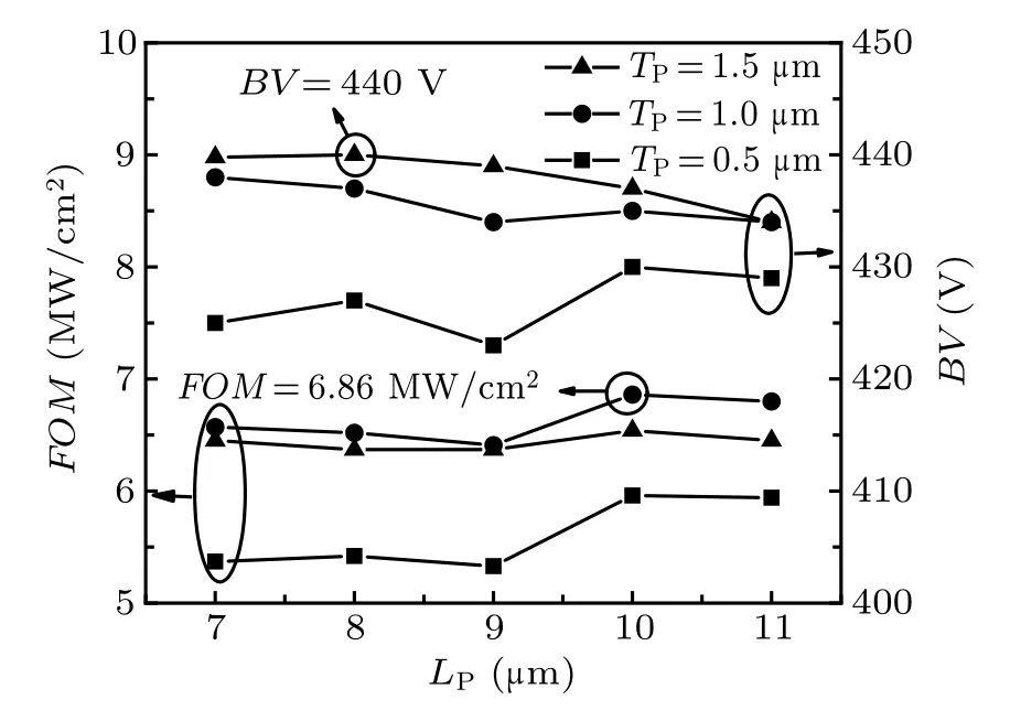
Fig.5. The relationship between FOM and BV of PBL Si/SiC LDMOS with LP.
The effect of the drift region length(LD)on BV,Ron,spand FOM of different devices is shown in Fig.6. Compared with Si/SiC LDMOS with deep drain region and the conventional Si LDMOS, PBL Si/SiC LDMOS has larger BV at the same LD. For Si/SiC LDMOS with deep drain region and the conventional Si LDMOS,the growth rate of BV decreases rapidly with LD;And PBL Si/SiC LDMOS has a steeper slope of BV compared with Si/SiC LDMOS with deep drain region and the conventional Si LDMOS. In addition, when LDis greater than 25 μm, PBL Si/SiC LDMOS has a smaller Ron,spthan Si/SiC LDMOS with deep drain region and the conventional Si LDMOS under the same LD. The growth rate of Ron,spof PBL Si/SiC LDMOS is slower than that of Si/SiC LDMOS with deep drain region and the conventional Si LDMOS.PBL Si/SiC LDMOS optimizes the surface lateral electric field and vertical electric field, which leads to an increase in BV and a reduction in Ron,sp. In addition,it can be seen from Fig.6 that when LD=20 μm, PBL Si/SiC LDMOS can take the maximum FOM value.
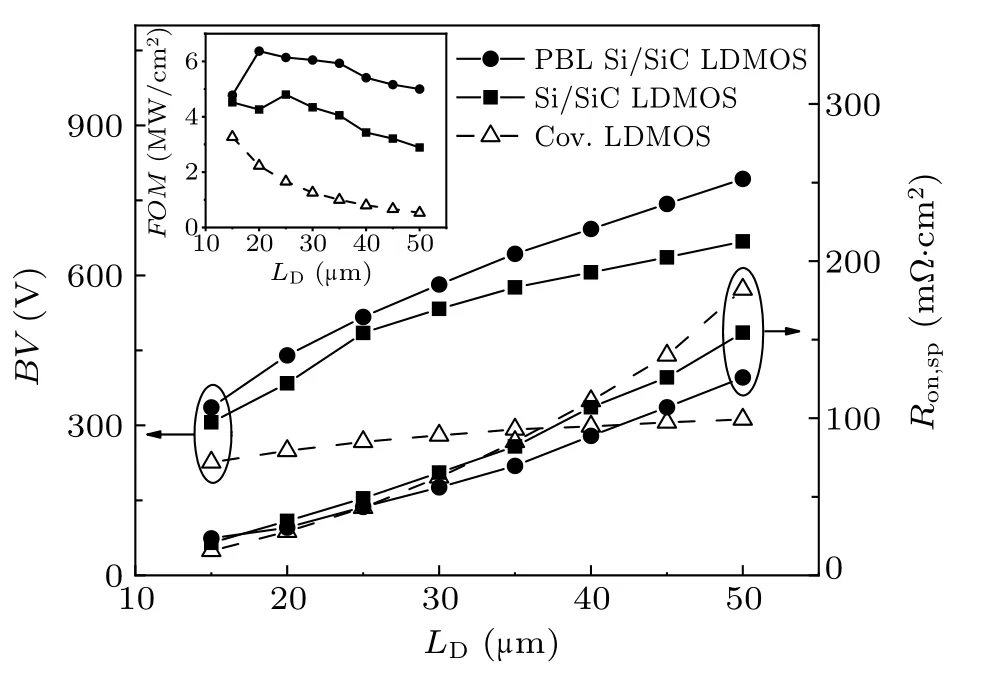
Fig.6. BV, Ron,sp, and FOM as a function of LD. Ron,sp is achieved@Vgs=10 V,Vds=20 V.
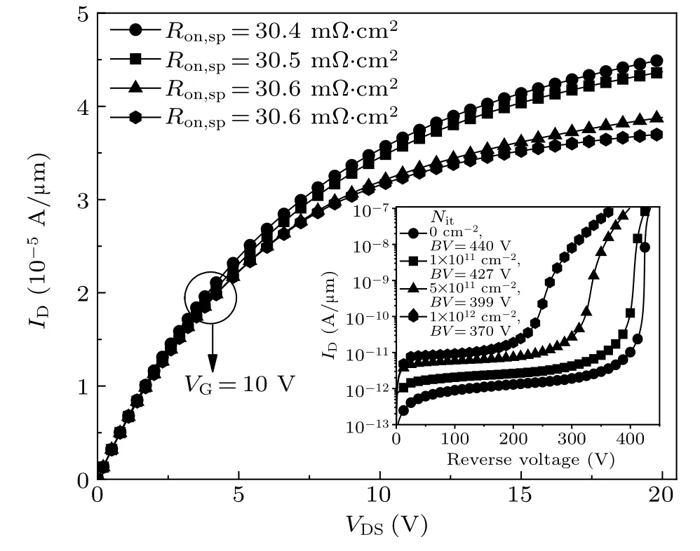
Fig.7. Forward I–V characteristics and reverse I–V characteristics of PBL Si/SiC LDMOS with different concentrations of interfacial charges.
According to the experimental results of literature,[20,21]the Si/SiC interface charges are introduced into the substrate fabrication process.[20,21]Therefore,this simulation considers the influence of acceptor-like traps in the interface on the performance of the novel device. As shown in Fig.7, the interface charges have little effect on the forward I–V characteristics of the device. It can be seen from Fig.7 that the specific on-resistance (Ron,sp) of the device changes very little under the three interface charges concentrations in this simulation.When the acceptor-like traps concentration(Nit)is lower than 1×1011cm?2,it has little effect on the BV of the device;when the Nitis higher than 1×1012cm?2,the device breaks down in advance. The BV is reduced from 440 V to 370 V, and the drain current increases rapidly,which fails to meet our design requirements. Therefore, improving the substrate fabrication process to reduce the acceptor-like traps density is the next step work.
Figure 8 shows the relationship between BV, Ron,sp, and ideal silicon limit for different devices. In the conventional LDMOS which satisfied the RESURF technology, the relationship between BV and Ron,spis Ron,sp∝BV2.[22]New structure breaks silicon limit at multiple drift zone lengths. The p-type buried layer makes the lateral electric field distribution of the device more uniform,resulting in an increase in the BV of the proposed device. At the same time, the p-type buried layer participates in the depletion of the drift region, so that the concentration of the drift region increases,which leads to a reduction in the Ron,spof the proposed device. Although the interface charges reduce the BV of the proposed device,when the Nitdoes not exceed 5×1011cm?2, PBL Si/SiC LDMOS still breaks the silicon limit.
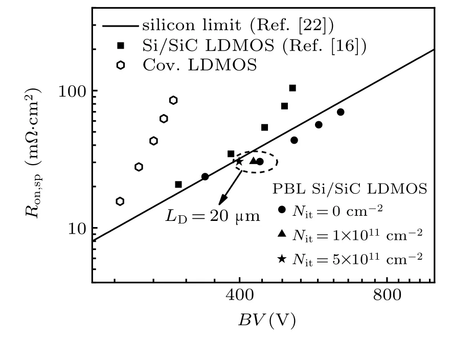
Fig.8. Ron,sp versus BV with the ideal silicon limit line. Ron,sp is achieved@Vgs=10 V,Vds=20 V.
4. Conclusion
In this paper,a novel Si/SiC LDMOS with a p-type buried layer has been proposed,which combines the electric field optimization technology of the p-type buried layer and the BPT terminal technology to increase the BV of the device and reduce the Ron.spof the device.The BV is significantly increased from 249 V of the conventional Si LDMOS to 440 V of the proposed structure with a drift length of 20 μm, while Ron.spis slightly increased. And the BV is increased from 384 V of Si/SiC LDMOS to 440 V of the proposed structure with a drift length of 20μm,and Ron.spreduces from 34.6 m?·cm2to 30.4 m?·cm2. The silicon limit is broken by PBL Si/SiC LDMOS.The influence of the p-type buried layer on the surface lateral electric field of the device and the influence of the drain region depth on the vertical electric field are studied. The high concentration of acceptor-like traps makes the BV drop. Reducing the acceptor-like traps density at the Si/SiC interface or eliminating the effect of the acceptor-like traps is the focus of future research.
猜你喜歡
農(nóng)業(yè)工程學(xué)報(bào)(2022年6期)2022-06-27 02:00:50
國(guó)畫(huà)家(2022年3期)2022-06-16 05:30:06
Chinese Physics B(2022年4期)2022-04-12 03:44:54
Chinese Physics B(2021年2期)2021-03-11 08:33:42
石材(2020年10期)2021-01-08 09:20:02
石材(2020年4期)2020-05-25 07:08:48
閱讀(低年級(jí))(2019年6期)2019-08-27 04:29:53
閱讀(低年級(jí))(2019年5期)2019-07-18 19:13:50
Asian Herpetological Research(2019年1期)2019-03-27 12:47:42
高中生·天天向上(2017年4期)2017-06-09 02:19:16
- Chinese Physics B的其它文章
- Quantum annealing for semi-supervised learning
- Taking tomographic measurements for photonic qubits 88 ns before they are created*
- First principles study of behavior of helium at Fe(110)–graphene interface?
- Instability of single-walled carbon nanotubes conveying Jeffrey fluid?
- Relationship between manifold smoothness and adversarial vulnerability in deep learning with local errors?
- Weak-focused acoustic vortex generated by a focused ring array of planar transducers and its application in large-scale rotational object manipulation?