
Review: Layer-Number Controllable Preparation of High-Quality Graphene for Wide Applications
2020-07-16 08:43:18YunBinXieMeiRongHuangandXinGuiLi
Yun-Bin Xie, Mei-Rong Huang and Xin-Gui Li
(1.State Key Laboratory of Pollution Control and Resource Reuse, and Shanghai Institute of Pollution Control and EcologicalSecurity, College of Environmental Science and Engineering, Tongji University, Shanghai 200092, China;2.Key Laboratory of Advanced Civil Engineering Materials of Ministry of Education, College of MaterialsScience and Engineering, Tongji University, Shanghai 200092, China;3.Shanghai Weikai Optoelectronic New Materials Co., Ltd., Shanghai 201111, China)
Abstract: Graphene, a well-known two-dimensional (2D) material, has sparked broad enthusiasm in both scientific and industrial communities in these years, due to its exceptional electrical, thermal, mechanical, and versatile properties. However, many properties and applications of graphene are layer-number dependent. The preparation of high-quality graphene with controlled layer numbers is full of challenge, since the layer number varies much with the synthesis routes and relevant experimental conditions. Hence, there is an urgent need to improve the layer-number controllability of graphene preparation. Generally, graphene can be prepared by two complementary approaches: “top-down” and “bottom-up”. Since they have their own advantages, the recent advances in the layer-number tunable preparation of high-quality graphene are separately studied from the two aspects in this review, especially those dedicated to single parameter. Some effective strategies are discussed in detail, mainly including 1) supercritical-CO2 assisted sonication, electrochemical exfoliation of graphite intercalation compounds, and layer-by-layer thinning with plasma or laser, for “top-down” graphene; 2) chemical vapor deposition (CVD) on dual-metal substrate, ion-implantation CVD, layer-by-layer CVD, plasma-enhanced CVD, layered-double-hydroxides template-assisted CVD; and 3) graphite-enclosure assisted epitaxial growth and pulsed-magnetron-sputtering assisted physical vapor deposition for “bottom-up” graphene on various substrates. In addition, the respective advantages of graphene with different layer numbers in properties and applications are also presented. Finally, the contribution concludes with some important perspectives on the remained challenges and future perspectives.
Keywords: graphene, nanosheet preparation, controllable layer number, tunable morphology, high quality graphene
1 Introduction
In the past decade, graphene, an emerging two-dimensional (2D) material ofsp2-bonded carbon honeycomb lattice, has become one of the most attractive topics in both research and industry sectors. It has exhibited excellent electrical, mechanical, thermal, and many other fascinating properties that result in versatile application potentials[1-4]. For example, its unique electrical properties (adjustable electrical conductivity as high as ~106S·m-1) and super-low density (as low as 0.03 g·cm-3) have made it one of the most promising light-weight electroconductive materials, as compared with the traditional metal conductors and the well-known conductive polymers such as polyaniline and polypyrrole[5-9].
However, most of the remarkable properties of graphene demonstrate strong layer-number dependence[2, 10]. Generally, compared with multiple-layer graphene, single-layer graphene (SLG) exhibits much better performance in electroconductivity, thermal conductivity, and transparency, as presented in Fig. 1(b)-(c). Nevertheless, some properties may reach the optimal value in few-layer graphene (FLG) rather than SLG, such as the Young’s modulus (Fig. 1(a)) and self-lubricating property (Fig. 1(d)).
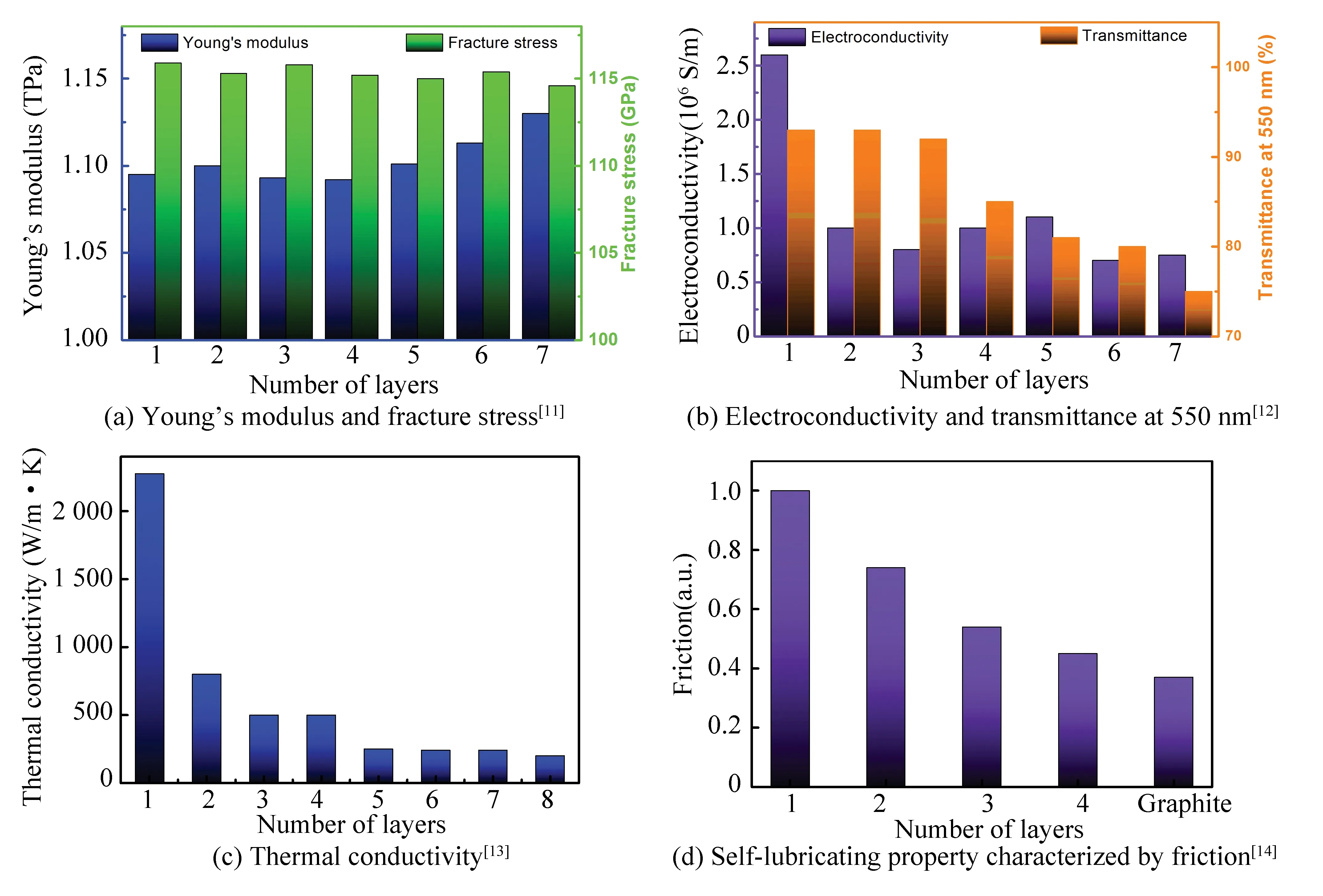
Fig.1 Layer-dependent properties of graphene
In addition, during the past years, more and more unique properties and application potentials have been found for graphene with few layers[15]. For example, due to its zero energy band-gap structure, SLG suffers from a serious current leakage in electronic devices, whereas the Bernal-stacked BLG and Rhombohedral-stacked three-layer graphene (TLG) have been found to perfectly solve the problem owing to opened bandgaps[16-18]. Besides, it is believed that TLG and four-layer graphene are more attractive in many applications, especially electronic and optical devices[19-20]. In addition, tunable optical and electrical properties can be easily achieved by FLG[21-22].
Hence, it is of great significance to synthesize graphene with different layer numbers-not only SLG, but also BLG, TLG, and FLG[23-24]. Particularly, it would be quite exciting if graphene with controlled layers could be prepared through the simple adjustment of certain parameter based on one method.
In general, graphene can be prepared by two classes of methods[25-26]: 1) The “top-down” approach, e.g., liquid-phase exfoliation which usually provides graphene in the forms of powder or dispersion, has great advantages in scalability and cost-efficiency as well as a very wide range of applications such as conducting additives in various composites[27-29]; 2) The “bottom-up” approach, usually referring to chemical vapor deposition (CVD) of hydrocarbons on metal substrates (e.g., nickel) and epitaxial growth on SiC, aims to prepare large-area and high-quality graphene that could be used in the future microelectronics industry[30-31]. Actually, these are two complementary strategies. For example, the production of transparent electrodes and sensors require large-area graphene, whereas graphene-based nanocomposites and energy storage devices ask more for bulk quantities of graphene[20].
However, both of them meet great challenge to synthesize high-quality graphene with desired layer numbers, due to their respective limitations[32-34]. For instance, the CVD growth of graphene is influenced by many factors such as the substrates, the carbon sources, and complicated process conditions, which brings about much uncertainty to the layer numbers and the thickness uniformity of the obtained graphene[33-34].
Many efforts have been devoted to the controllable synthesis of graphene in the past several years, including the strategies for the preparation of graphene with controlled morphology or doping levels[35-36]. However, no systematical review focused on the layer-number controllability of high-quality graphene has been found so far. For an overall understanding and further promotion of the controllable preparation of graphene, here the recent progress on the layer-number controllable preparation of graphene is reviewed based on the above two methods, focusing on the synthesis strategy for high-quality pristine graphene. In this work, the quality of graphene is largely assessed by two indexes: 1) lateral size, which is usually characterized by TEM or AFM and expected to be greater than a few micrometers; 2) defects level, indicated by the intensity ratio of the Raman D (ID) and G (IG) peaks (ID/IG), where a smallerID/IGvalue suggests a lower defects level. In the same way, the layer numbers or thickness of graphene can be judged from the intensity ratios ofI2D/IG, where a higherI2D/IGvalue corresponds to thinner graphene-layer[37-38]. Obviously, for high-quality graphene, both a larger lateral size and lower defects level are preferred[20].
2 Layer-Number Controllable Preparation of “Top-Down” Graphene
Here, the “top-down” graphene refers to the graphene exfoliated from graphite by top-down methods such as liquid-phase exfoliation. The biggest advantage of “top-down” graphene over “bottom-up” graphene lies in that it can be deposited on different substrates and used in a variety of environments[26]. Especially, it can be employed to produce graphene-based composites or films, which greatly broaden the application of pristine graphene. Besides, top-down methods usually exhibit greater potentials in scalable production of graphene in large quantity. Therefore, studies on the controllable synthesis of top-down graphene are not only necessary but also of great significance.
2.1 Liquid-Phase Exfoliation
Liquid-phase exfoliation refers to the exfoliation of graphite in liquid media such as some proper solvents (e.g.,N-methyl-2-pyrrolidone) or surfactants (e.g., sodium dodecyl sulfate). It is well-recognized as a versatile and scalable method to produce graphene nanosheets (GNS). GNS can be extensively employed to produce composites for various applications, such as thin-film transistors, conductive transparent electrodes, light-emitting diodes, and photovoltaics[39-44]. However, there are so many factors that influence the exfoliation and stability of the GNS, such as the type of the starting graphite and the liquid media, as well as the energy density and duration of sonication[22, 45-47]. Thus, it is of great challenge to prepare high-quality GNS with controlled layer numbers by this method, and only a few studies can be found[22, 48-49].
Wang et al.[50]reported the successful synthesis of layer-number controllable GNS using ultrasound in supercritical CO2, which can easily diffuse between the graphene layers due to its high diffusivity, low viscosity, and small molecule size[49, 51]. It has been demonstrated that the electrical conductivity of FLG exfoliated by shear-assisted supercritical CO2can reach a high level of 4.7×10⁶S/m[52]. Ultrasonication can further weaken the van der Waals interactions between the graphene layers and urgent need thus effectively exfoliate the graphite into thin GNS. It is well-recognized that the efficiency of exfoliation is greatly influenced by the power of ultrasonication. In virtue of the coupled effects of supercritical CO2and ultrasonication, they successfully prepared SLG, BLG, and FLG through 30 min-ultrasonication with preset ultrasonic power of 300 W, 120 W, and 60 W, respectively (see Ref.[50]). That is to say, in the highly-diffusive environment, the layer numbers of GNS can be controlled by the ultrasonic power. In addition, LiFePO4/graphene composite cathode made from the as-exfoliated GNS exhibited remarkable electrochemical performance. The specific capacity was reported to be 160 mAh/g which is 94.7% of the theoretical capacity. The problem lies in that the lateral size of the obtained SLG (50 - 100 nm) turned to be quite small due to the enlarged ultrasonic power. Nevertheless, it really demonstrates the advantages of supercritical CO2in the controllable preparation of graphene with desired layer numbers.
It should be noted that the liquid-phase exfoliated GNS usually turns out to be a mixture that consists mainly of FLG and only a small fraction of SLG[20]. To improve the productivity of SLG, Kovtyukhova et al.[53-54]introduced a self-made Br?nsted acid-intercalated graphite compounds as the starting material. The compounds were a mixture of graphite and 85 wt% H3PO4that was coated on glass slides and kept at 120 ℃ for enough intercalation which could reduce the interlayer cohesive energy and facilitate the exfoliation to monolayers[54]. After a systematic study on the medium polarity protic solvents such as isopropanol andn-pentanol, together with the temperature and the duration of the exfoliation process, they successfully obtained a yield of almost 100% SLG. Meanwhile, thanks to the gentle enough exfoliation process that would not disrupt thesp2π-conjugated system of graphene and preserve the crystalline integrity of graphene, the lateral size of the obtained SLG was as large as tens of microns. Although the preparation period of at least 2 days seems too long, it opens another door for the preparation of graphene with high yield of SLG together with good quality.
2.2 Electrochemical Method
Electrochemical exfoliation is a relatively simple, economic, and environment-friendly method. However, it had been less explored to prepare graphene nanosheets, due to the relatively numerous defects produced during the electrochemical process[32, 55]. Only till the past few years, it received increasing attention as a potential scalable method for the preparation of graphene[56].
To decrease the defects of graphene, Alanyalioglu et al.[55]chose SDS solution as the electrolyte in the electrochemical exfoliation graphite, which could adsorb on the surface of graphene sheets and therefore prevent them from re-stacking.It was pointed out that the exfoliation could be ascribed to the horizontal intercalation of dodecyl sulfate anion (electrolyzed from SDS) into the basal plane of graphite. The mobility and concentration of these anions could be tuned by the electrode potential. Thus, the layer numbers of graphene could be adjusted by the potential value for SDS intercalation into graphite. When the applied potential increased from 1.4 V to 2.0 V, the intensity ratio of the Raman 2D-band to G-band (I2D/IG) increased rapidly from ~0.15 to 0.31, which implied an obvious decline of the graphene thickness. According to the TEM results, the average size and thickness of the GNS prepared at 2.0 V were around 0.5 μm and 1 nm, respectively, indicating that SLG could be achieved under a high potential value for intercalation. In addition, the finalID/IGratio was found to be 0.12 which was quite close to that of the raw graphite (0.006), implying a low level of defects. Moreover, the obtained graphene/SDS suspension exhibited quite good stability for 8 months with no precipitation observed. However, it is a pity that the obtained graphene was a mixture of FLG and few SLG even after centrifuge, rather than graphene of certain layer(s) with narrow distribution.
For a better control of the graphene layer numbers, Wang et al.[32]introduced another strategy named lithium conversion electrochemical reaction, based on a series of graphite intercalation compounds (GICs) which could be easily synthesized on a large scale. Firstly, CuCl2-FeCl3-GICs with different stage numbers were prepared by the insertion of CuCl2-FeCl3layer between the graphite layers through a melt-salt method, which involved the calcination of the mixture of anhydrous FeCl3, anhydrous CuCl2, and natural graphite in a sealed reactor at 550-600 ℃ for 12 h. By adjusting the content of the reactants and the conditions of heat treatment, GICs with different stage numbers of 2, 4, and 6 were achieved. Then, the GICs were introduced as working electrode for electrochemical exfoliation (see Ref.[32]). After an initial discharge/charge process, the compounds converted to a sandwiched composite in which the CuCl2FeCl3FeCu layer was inserted between graphene layers. Since the van der Waals forces of adjacent graphene sheets were destroyed, individual graphene layers could be simply exfoliated solely by a mild sonication. Accordingly, the graphene nanosheets with 2, 4, and 6 layers were successfully prepared by utilizing the GIC with stage number of 2, 4, and 6, respectively. In addition, the obtained BLG had a large lateral size of ~8 μm from the TEM image, and exhibited a high electron mobility of about 4 000 cm2V-1s-1at room temperature. Notably, no oxygen functional groups or defects were produced during the whole process, as proved by the TEM, AFM, and Raman results in Ref.[32]. Although SLG was not available, it opens up a new avenue for producing high-quality graphene in a large scale.
2.3 Layer-by-Layer Thinning
In 2010, Huang et al.[57]demonstrated that graphene can be peeled layer-by-layer using Joule heating from transmission electron microscopy (TEM). Although it was far away from practical device fabrication, this broke a novel path in reducing the thickness of graphene to achieve desired layer numbers by the use of proper energy such as plasma and laser treatment[58-60].
2.3.1Plasmathinning
Plasma etching technique is a quite effective tool in thinning layered materials, which utilizes the direct bombardment effect of precursor gases such as nitrogen, argon, hydrogen, etc. under proper energy of plasma treatment[58-59, 61]. The gases and plasma energy is quite important, otherwise the obtained graphene may be inhomogeneous or have too much defects[59].
Zhang et al.[61]demonstrated the successful plasma-thinning of graphene from multiple to single layers on a semiconducting substrate of SiO2/Si at room temperature. They utilized medium input power (300-500 W) which is strong enough to etch graphene layers but less invasive, and chose hydrogen and argon (Ar) as the precursor gas. Owing to its heavy molecular mass of 40 g·mol-1, Ar has a high kinetic energy which is large enough to destroy thesp2-bonded hexagonal structure of graphene. Besides, since Ar is easy to be dissociated, it is of great efficiency that can etch multiple layers in a short time. As for hydrogen with much smaller mass (2 g·mol-1), it has relatively weaker ion bombardment effect which can be used to layer-by-layer etch for SLG with high precision. Hence, the thinning process was conducted by two different etching modes: one was the fast etching mode by Ar plasma, through which thick graphite flake could be etched into 5-layer graphene at a speed of 7-8 layers/min; the other was the fine mode of layer-by-layer etching with H2plasma.
By simply tuning the fast and fine etching modes, accurate control over the layer numbers of graphene could be achieved. TLG, BLG, and SLG were obtained after three consecutive fine etching for 2 min, 1 min, and 1 min, respectively (Fig.2)[61]. For all the obtained graphene with different layer numbers, it was successfully observed that large-area, uniform films covered all the domains across the sample. However, the defects level should not be ignored, as evidenced by the highID/IGratio of ~1.05 for SLG, although post annealing was introduced to effectively heal the defects produced by ion bombardment. Nevertheless, it is a less-invasive method that could be applicable in graphene-based device fabrication, since it has no obvious etching effect on the SiO2/Si substrate.
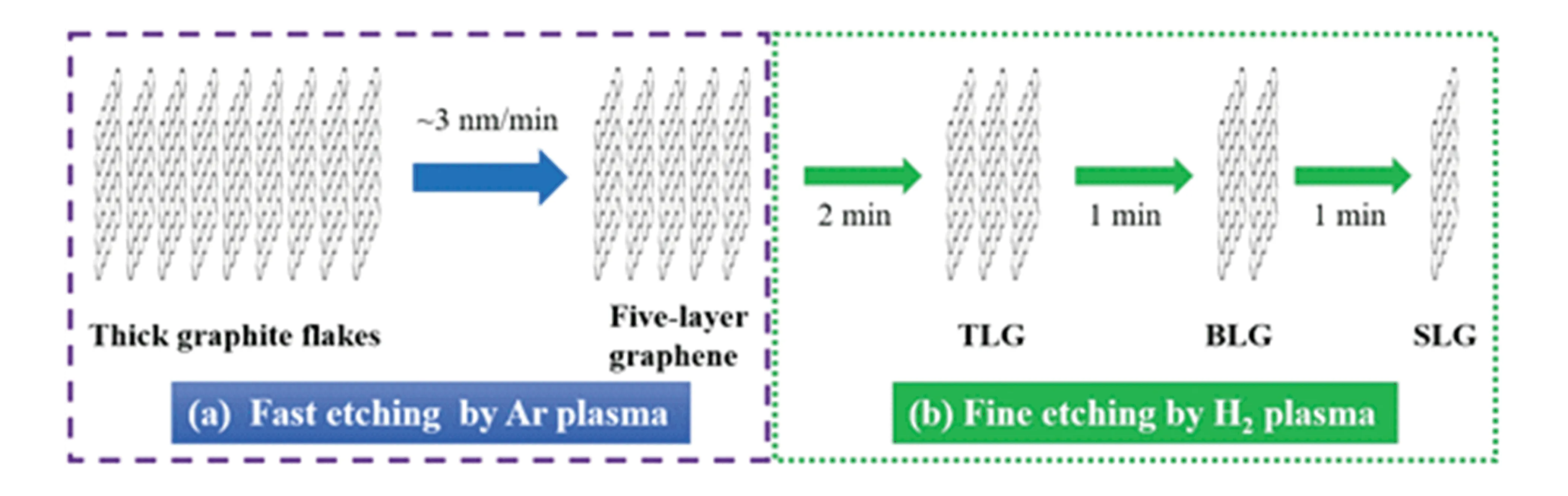
Fig.2 Scheme of the plasma-thinning process from multiple-layer graphene to desired single-to-few layer graphene[61]
2.3.2Laserablation
High-frequency laser has also found to be effective for the exfoliation of graphite[62-63]. Han et al.[60]found that FLG with 4 - 7 layers can be etched to SLG under reasonable laser power density.
To further enhance the layer-number controllability, Lin et al.[63]demonstrated an accurate control of layer-by-layer thinning 5-layer CVD-graphene through picosecond laser radiation, as illustrated in Fig. 3. Since the photon energy of the laser (1.2 eV) was much higher than the van der Waals force between the graphene interlayers (0.17 eV), the peeling-off process was able to start from the grain boundaries of the CVD graphene defects (Fig.3(c)). Subsequently, the van der Waals force would be rapidly weakened along with the increase of the distance between the interacting grains and the adjacent layers, which finally led to the peel-off of the graphene. To obtain a specific layer-number graphene, the laser energy density should be adjusted to the level higher than the corresponding threshold, such as ~1.0 J/cm2for SLG and ~0.5 J/cm2for 4-layer graphene (Fig.3(b)). By simply changing the pulse threshold energy, specific layer numbers from four to single layers were achieved in a controllable way.
It is worth notice that the formation energy of the C-C bond (3.7 eV) of the graphene is much higher than the photo energy. The graphene structure would not be broken in the whole process. As a result, the obtained graphene exhibited very few defects, as evidenced by the smallID/IGvalue of less than 0.07.More importantly, it can be conducted in atmospheric condition in a simple, non-contact, and patternable way. Therefore, although graphene grain size was relatively small (normally about 1 μm, dependent on the CVD process), it is really an attracting method for the fabrication of graphene-based electronic devices.
In short, for the “top-down” methods based on the exfoliation of graphite, to achieve high-quality graphene with controlled layer numbers, the key point is how to break the van der Waals force between the graphene interlayers in a proper way. On the one hand, no matter by ultrasonication, plasma, laser, or other energy, sufficient energy density is required to overcome the interaction between graphene layers (as presented in Fig. 3(b)). On the other hand, the energy applied should not be too high to destroy the graphene structure. Besides, effective measures should be taken to prevent the re-stacking of exfoliated GNS.
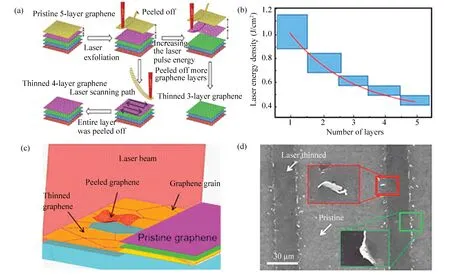
Fig.3 (a)Schematic image of laser ablation process (b) Thresholds of the laser energy density for graphene with 1-5 layers (c) Scheme of the mechanism of laser ablation (d) SEM image of the graphene after laser ablation: the peeled-off graphene grains (marked in the red box) and the graphene grain residues (in the green box)[63](Adapted with permission from Ref.[63].Copyright 2015,Springer)
3 Layer-Number Controllable Synthesis of “Bottom-Up” Graphene
“Bottom-up” graphene usually refers to the large-area graphene film synthesized by CVD growth on metal substrates or epitaxial growth (EG) on SiC. It has exhibited huge potentials in the application of future microelectronic industries, such as FETs, touch panels, and photovoltaic devices, especially the electrical interconnects in large-scale integrated circuits[25, 26, 30]. Since graphene with different layer numbers can enrich the adjustability in versatile applications, some efforts have already been devoted to the preparation of large-area graphene with controlled thickness. The strategies, the carbon sources, the substrates, as well as the layer numbers, and quality of the obtained graphene are summarized in Table 1 .
3.1 Chemical Vapor Deposition
CVD synthesis of graphene has been regarded as one of the most important techniques for high-quality graphene with large area and few defects[30, 33, 73-75]. The typical process of CVD-graphene usually consists of three steps, i.e., carbon dissolving, thermal annealing, and transfer process (usually by PMMA)[33], as illustrated in Fig. 4. It is so complicated a system that the CVD growth of graphene tends to be influenced by many factors, at least including 1) the species, structure, and concentration of carbon sources[76-78]; 2) the carbon solubility and crystallinity of the substrate[21, 33, 79-82]; 3) the process parameters, such as the gas flow ratio and rate, the growth and annealing temperature, the chamber pressure, the deposition time, the cooling rate, and so on[21, 23, 78, 83-84].
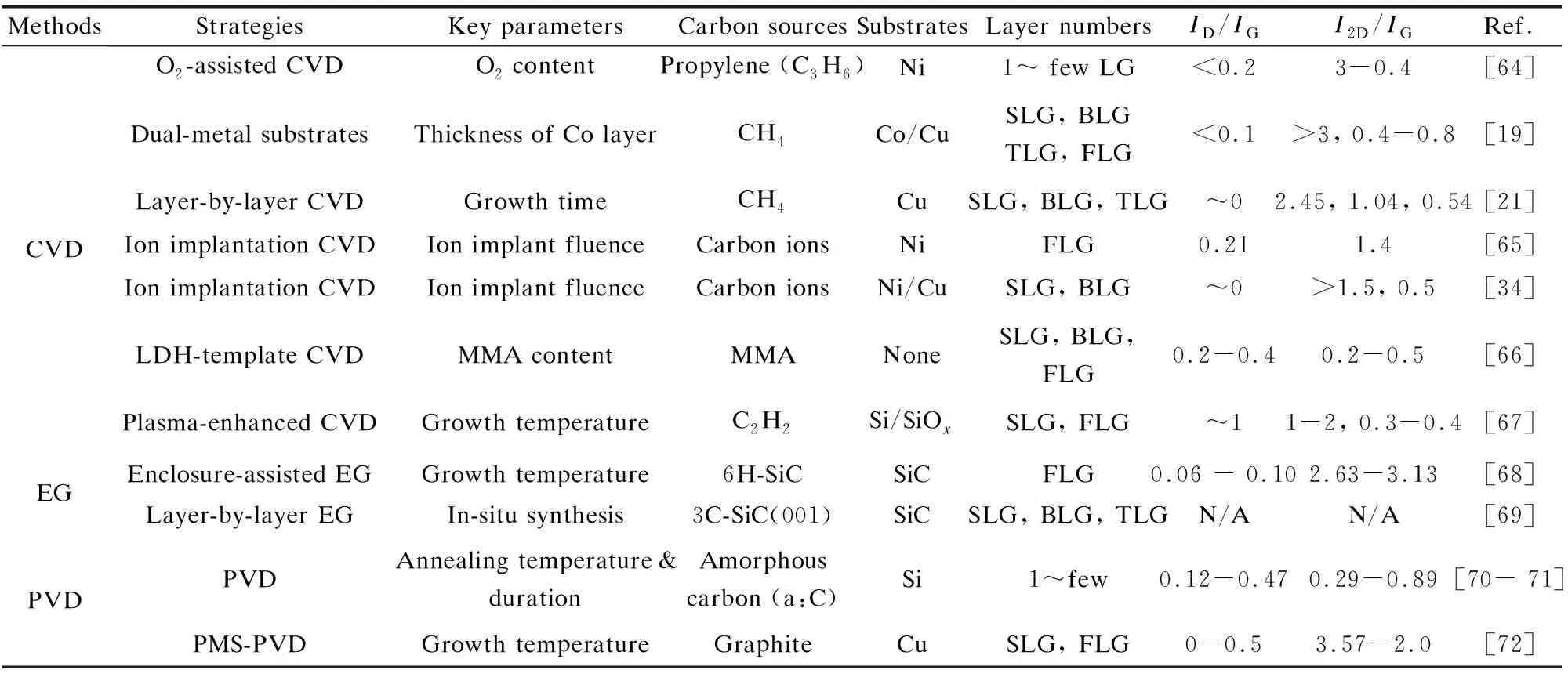
Table 1 Methods for the layer-number control of graphene synthesized by “bottom-up” approaches
Note: CVD = chemical vapor deposition; EG = epitaxial growth; PVD = physical vapor deposition; PMS-PVD = pulsed magnetron sputtering PVD; N/A = not available.
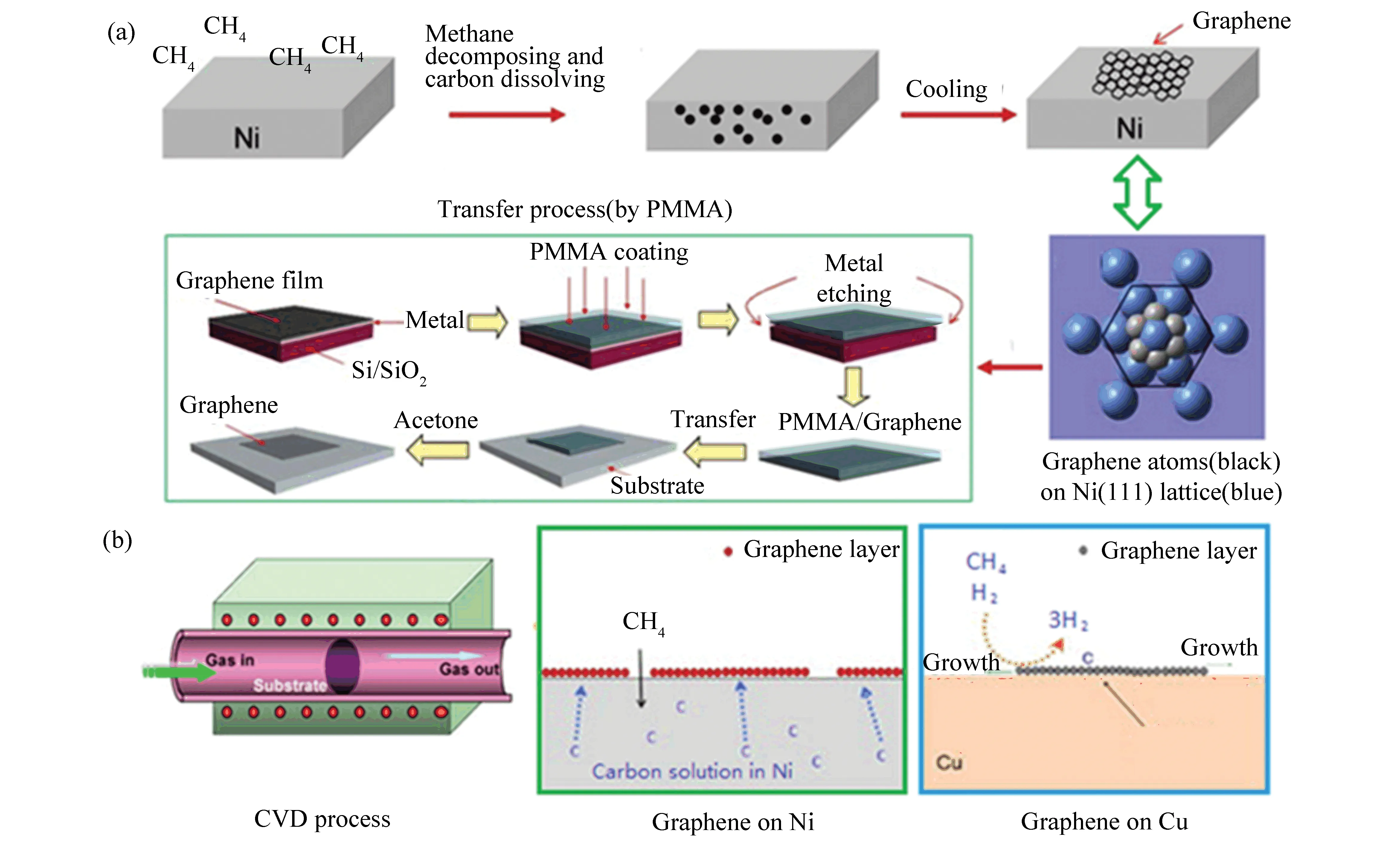
Fig.4 (a) Schematic image of the synthesis of graphene by CVD process (b) The differences in the mechanism of CVD-growth of graphene on Ni versus Cu[33] (Adapted with permission from Ref.[33]. Copyright 2013,American Chemical Society)
Therefore, the CVD synthesis of high-quality graphene with controlled layer numbers is quite challenging. Nevertheless, some effective methods have been developed to solve this problem, such as introducing composite substrates, layer-by-layer CVD, ion-implantation CVD, template-assisted CVD, as well as plasma-enhanced CVD[19, 21, 34, 66, 67].
3.1.1Dual-metalcatalyzedCVD
Studies on CVD growth of graphene have been extensively focused on two kinds of metal substrates with different carbon solubility. However, both of them have limitations in layer-number controllability. For the CVD growth of graphene based on the metals with high solubility to carbon (e.g., Ni, Co, and Ru), which refers to precipitation process after surface segregation, the problem lies in the nonequilibrium-precipitation process which makes great challenges to tune the layer numbers of graphene. In contrast, for metals with low solubility to carbon (e.g., Cu, Pt, and Ge), the CVD growth of graphene tends to yield SLG rather than FLG since it follows a self-limiting surface mechanism[19, 34].
Dual-metal substrates that combine the benefits of the two kind of metals with different carbon solubility have been found effective for enhancing the controllability of CVD growth[19, 34].
In virtue of Co-coated Cu foil substrates, Lin et al.[19]presented that the layer-number of CVD-graphene can be precisely tuned by changing the thickness of the Co layers. The Co layer with moderate carbon solubility was designed as a carbon-dissolving place for graphene growth, while the Cu layer with low carbon solubility as carbon-rejecting layer. The carbon solubility of the composite substrate was successfully adjusted by regulating the thickness of the Co layer. As a result, uniform SLG, BLG, TLG, and FLG with few defects were obtained by varying the thickness of the Co layer to 80 nm, 130 nm, 205 nm, and 400 nm, respectively[19]. It was found that the graphene thickness seemed insensitive to growth temperature and time. Besides, the obtained SLG films demonstrated high quality together with a high yield of 98%. The as-synthesized AB-stacked BLG and TLG were defects free and had a high surface coverage of 99%. In addition, the obtained graphene of 1-6 layers exhibited excellent layer-dependent properties, such as low electrical sheet resistance of 865-282 Ω/sq, together with high transmittance at 550 nm of 97.3%-84.9%.
However, it has been pointed out that the controllability of this method is still limited, since it is not easy to decouple the carbon adsorption and precipitation processes that are thermally driven and occur simultaneously[34, 85].
3.1.2Layer-by-layerCVD
Han et al.[21]developed a layer-by-layer technique to prepare CVD-graphene with desired layer numbers in a precisely controllable way. This method is based a novel two-heating zone CVD consisting of two-step procedures, see Ref.[21]. The first step was the growth of SLG as the conventional CVD did on Cu substrate with 10 sccm of CH4gas flow and 300 sccm of H2gas flow, at 1 Torr and 1 040 ℃ for 10 min. The followed step was layer-by-layer growth of graphene on the as-grown monolayer under optimized experimental parameters. In virtue of the van der Waals epi-growth of 2D layered materials, layer-by-layer growth of monolayer graphene on the as-synthesized layer was successfully achieved through simply tuning the growth time. It turned out that BLG and TLG completely covered the previous layer at the growth time of 60 min and 120 min, respectively (see Ref.[21]). The obtained SLG, BLG, and TLG were found in good quality with uniform thickness distribution and free of defects, as revealed by the Raman spectra in Ref.[21]. More importantly, these outputs exhibited outstanding optical and electrical properties. The transmittance at 550 nm was recorded to be 97.4% for the SLG and down to 83.7% for 7-layer graphene. The sheet resistance was 723 Ω/sq for SLG and subsequently decreased with the increase of the layer numbers.
3.1.3IonimplantationCVD
Ion implantation CVD refers to a pre-implantation of carbon species in the metal substrates, ahead of the high temperature annealing and quenching processes[34, 65]. As a mature technology in the microelectronic industry, ion implantation has grand advantage in controlling the content of carbon atoms, which may significantly improve the controllability of graphene thickness. However, for the substrates of single metals such as Ni and Cu, it is not so satisfactory that the layer numbers of the obtained graphene are uneven, and the correlation between the carbon fluence and graphene thickness is not strictly followed[86].
Aiming to enhance the controllability over the quality and layer numbers of CVD graphene, Wang et al.[34]adopted a dual-metal substrate, i.e., Ni-coated Cu foils (a 300-nm-thick Ni layer deposited on Cu foil). Since the final formation of graphene was on Cu-like alloy and the concentration of Ni was negligible, the graphene thickness was less sensitive to the thermodynamic process. Therefore, combining the advantages of the composite substrate and the precise implantation of carbon ions, it can be expected to achieve a stricter dependence of graphene thickness on the carbon fluence. In other words, it can be precisely controlled by simply tuning the dosage of carbon ions pre-implanted.
As illustrated in Ref.[34], carbon ions with predesigned fluence were implanted into the Ni layer of the Ni/Cu alloy. During the thermal treatment of CVD process, interdiffusion of Cu and Ni atoms occurred and carbon atoms were expelled to the surface due to its poor solubility in Cu. Ultimately, uniform SLG and BLG were formed on the surface under the carbon ion implant fluence of 4×10¹⁵and 8×10¹⁵atoms·cm-2, respectively. In addition, since the carbon ion was able to precipitate under steady temperature, defect healing of graphene could be achieved, which produced high-quality graphene with excellent crystalline and uniformity. The obtained graphene turned out to be almost free of defects, as evidenced by the negligible presence of Raman D-band. Furthermore, the SLG and BLG films exhibited excellent carrier mobilities (2 000-4 000 cm2V-1s-1for holes and 1 000-3 500 cm2V-1s-1for electrons), which indicates a bright application potential in graphene-based nano electronic devices.
3.1.4Plasma-enhancedCVD
Since the traditional CVD-graphene requires too high growth temperature (usually 800-1 000 ℃), plasma-enhanced CVD (PECVD) has attracted more and more attention as a solution to low-temperature growth of graphene (~600 ℃)[87-88]. Different from the traditional CVD system, PECVD mainly consists of three component parts, including the gaseous system, the plasma generator system, and the vacuum heating system (Fig. 5(a)). According to the power source for plasma generation, the key component, the plasma generator, is usually categorized into three types, i.e., microwave plasma (~2.45 GHz), radio frequency plasma (~ 13.56 MHz), and direct current plasma. It is a catalyst-free synthesis method that can be applied to the growth of graphene on not only metal substrates, but also dielectrics such as SiO2and Si[89]. However, since it contains various kinds of species and reactions that greatly influence the morphology and thickness of graphene, the control of layer numbers is not an easy work[89].
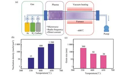
Fig. 5 (a)Schematic illustration of plasma-enhanced CVD[89]. (b,c) The dependences of nucleation density (b) and grain size (c) on temperature[67](Adapted with permission from Ref.[67].Copyright 2018,Royal Society of Chemistry)
However, it must be noted that it is so complicated a process that requires accurate control of the interaction with the SiOx. Besides, the quality is still under the thumb of the high nucleation density, which would lead to relatively low device performance. In addition, the growth rate is too low (below 10 nm·min-1) for industrial-scale production. Nevertheless, it proposed a low-temperature solution to the controllable synthesis of high-quality CVD graphene on dielectric materials.
3.1.5Template-assistedCVD
For the controllable growth of CVD graphene, Sun et al.[66]designed a novel 2D template, named layered double hydroxides (LDH), for the synthesis of graphene nanosheets in the interlayer galleries.
The LDH templates were prepared as follows: 1) Dissolve the mixture of Mg(OH)2·6H2O and Al(OH)3·9H2O in deaerated water; 2) Add methyl methacrylate (MMA) and dodecyl sulfonate (DSO) to form an emulsion; 3) Add NaOH into the emulsion and reacted at 80 ℃ for 8 h; 4) Dry the precipitate filtered at 50 ℃ for 10 h. Here, MMA acted as the carbon source, whereas the role of the DSO was to support the layers and provide space for MMA.
Subsequently, the intercalated MMA was calcined into graphene by H2/Ar at 900 ℃ for 2 h. As shown in Fig.6, it was believed that the confined 2D interlayer of LDH provided suitable space for the formation of graphene. By adjusting the quantity of MMA intercalated in the layered precursor, SLG, BLG, and FLG were satisfactorily synthesized in the interlayer.
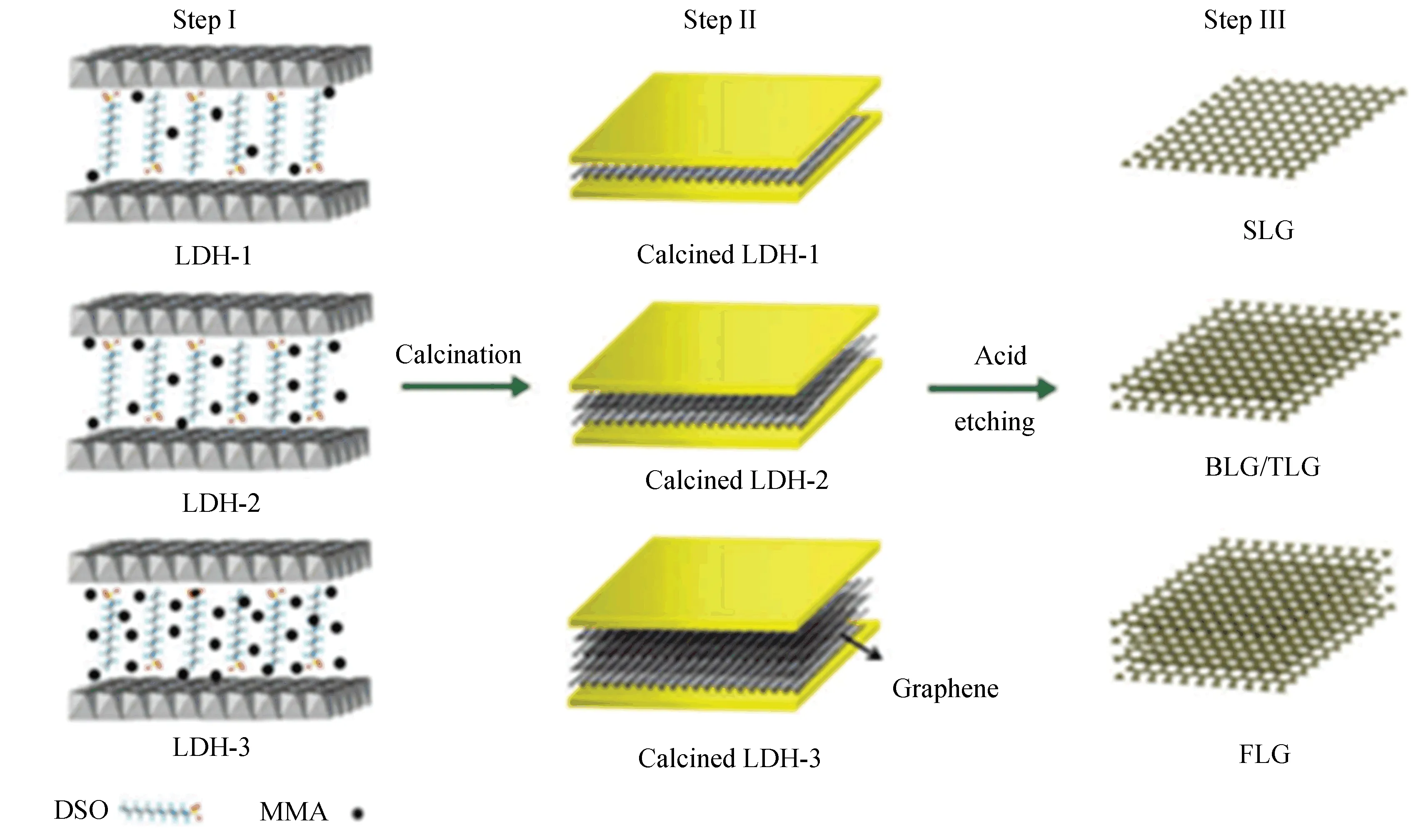
Fig.6 Scheme for the CVD synthesis of graphene with controlled layer numbers by template of layered double hydroxides (LDH) with different molar ratios of MMA to dodecyl sulfonate (DSO), marked as LDH-1 (1.2), LDH-2 (3.2), and LDH-3 (8.0), respectively[66](Reprinted with permission from Ref.[66].Copyright 2012, Royal Society of Chemistry)
Finally, GNS dispersion was easily obtained by dissolving the metal oxide phase in hydrochloric acid. Notably, the first advantage of this method lies in that it avoids the complicated transfer process of traditional metal-catalyzed CVD method. Besides, since the LDH precursor can be made from cheap materials that are readily available, it is cost-efficient and easy to scale-up. Although the defects cannot be ignored according to the strong Raman D-bands, and the properties such as electrical conductivity need to be further evaluated. It surely provides another option for the layer-number controllable CVD synthesis of graphene without transfer process.
3.2 Epitaxial Growth on SiC
The biggest shortage of CVD graphene lies in the transfer process from the metal substrates to the desired substrates, which brings many defects and impurities that may deteriorate the final properties. In fact, for successful electronic applications, graphene must be synthesized on semiconductive or insulative substrates, such as silicon wafers and glasses[90]. Hence, much attention has been paid to the epitaxial growth of graphene on the semiconductive SiC, which can be directly used in high power, high frequency, and high temperature devices such as LEDs[91-92].
“Epitaxial growth” means the growth of a crystalline layer on a crystalline substrate which follows the structure of the substrate. Since Si has a higher vapor pressure than C in SiC, large-area and high-quality graphene can be achieved by thermal decomposition of SiC single crystal under a high degree of vacuum. It was reported that the domain area of epitaxial graphene on SiC could be as large as 200 μm×200 μm, which is much larger than that prepared by other methods[93-94].
However, many factors have been found to influence the growth and properties of epitaxial graphene. First of all, the two polar faces of SiC(i.e., C-face and Si-face) exhibit quite different properties during the growth of graphene. The Si face has advantages in the thickness control and homogeneous growth of graphene due to the slow growth rate on the Si face, but the low charge carrier mobility of the obtained graphene is not satisfactory[68, 92]. As for the C face, although the electronic properties of the obtained graphene can be close to the mechanically exfoliated graphene films, the thickness of C-face graphene increases sharply with the elevating of graphitization temperature[95]. Besides, the thickness of the epitaxial graphene varies with many process parameters, such as the vacuum conditions, the growth temperature, and its duration, and so on[96-97]. Therefore, it is not easy to obtain epitaxial graphene on SiC with desired layer numbers and high quality in a controllable way.
For a better controllability over the thickness of epitaxial graphene, Hu et al.[68]introduced a graphite enclosure into the epitaxial growth process on the C-face of 6H-Si C. The graphite enclosure was designed to provide a relatively high and dynamically balanced Si partial pressure, so as to slow down the growth rate and enhance controllability of graphene growth. Specifically, the 6H-SiC was firstly etched by hydrogen at 1 600 ℃ in H280 L/min and C3H85 mL/min for 7 min. Then, the H2-etched SiC samples were put into the graphite enclosure for epitaxial growth under~10-3mbar. As the graphitization temperature elevated from 1 300 to 1 600 ℃, the thickness of epitaxial graphene exhibited a slow climb from 0.4 to 3.8 monolayers. That is to say, the layer numbers of the epitaxial graphene became tunable with the help of the graphite enclosure. In addition, along with the elevation of the growth temperature, the stacking, homogeneity, and continuity, as well as the crystalline quality were improved a lot. Therefore, the obtained graphene exhibited quite good quality, as evidenced by the homogeneous coverage, large domain size of ~3 μm, and small RamanID/IGratio of 0.06.
It should be mentioned that more accurate control over the thickness of epitaxial graphene has been realized in the lab, with the aid of some advanced instruments[69, 98]. For example, Aristov et al.[69]demonstrated the layer-by-layer synthesis of epitaxial SLG, BLG, and TLG on 3H-SiC/Si(001) wafers, utilizing LEED and high-resolution spectroscopy equipped with fast dynamic-XPS synchrotron facilities. The epitaxial growth of graphene occurred in the fast dynamic-XPS stations, while its thickness was real-time controlled by the micro-spot XPS according to the C1s core level spectra. More importantly, the synthesis procedure would stop once a desired layer numbers of graphene was gained. Therefore, the layer-by-layer growth of graphene can be achieved “automatically”, without following a particular recipe of the process parameters as the traditional epitaxial-growth method does.
3.3 Physical Vapor Deposition
Physical vapor deposition (PVD) is a low-cost, convenient, and scalable method for fabricating large-area uniform films[99-100]. Thus, it is of great potential to study the controllable preparation of graphene in this field[72, 101].
Narula et al.[70-71, 102]investigated the PVD growth of graphene on Cu using radio frequency (RF) and direct current (DC) sputtering technology. The method they developed consists of 4 steps: 1) deposition of amorphous carbon (a-C) thin film (12 - 60 nm) on Si substrate by RF sputtering; 2) deposition of Cu nanoparticles (800 nm) on the as-deposited a-C films by DC sputtering; 3) growth of graphene on the top of the Cu film under necessary sputtering energy by the catalysis of the sputtered Cu thin film; 4) annealing in hydrogen environment at 1 020 ℃ for 50 min under a low pressure of 1 Torr[103]. Based on a systematic study of the complicated factors, they suggested that relatively lower annealing temperature and shorter duration are more helpful for lowering down the thickness of the obtained graphene. When the annealing temperature decreased from 1 020 ℃ to 920 ℃ for the same duration of 50 min, theI2D/IGratio increased from 0.9 to 1.6, which indicated the presence of multi-layer graphene with more than 10 layers and FLG with 3-9 layers, respectively. After a further reduction of the duration time to 20 min at 920 ℃, theI2D/IGratio increased to 2.6, indicating the presence of SLG[102]. Therefore, graphene with different layers can be obtained by carefully adjusting the annealing temperature and duration.
To further improve the quality of PVD graphene films, Vijayaraghavan et al.[72]introduced a so-called pulsed magnetron sputtering (PMS) technique. Compared with DC and RF sputtering, PMS exhibited higher adatom mobility, surface diffusion, and deposition rate. The PMS of graphite was carried out in an argon atmosphere with high-purity of 99.999%, under a base pressure of 4.5×10⁻⁴mTorr. Carbon atoms from the graphite were sputtered on to a Cu foil and deposited to form graphene films under different growth temperature. It was found that the thickness of the graphene film was directly influenced by the deposition temperature. As the deposition temperature increased from 700 to 920 ℃, the RamanI2D/IGratio increased almost linearly from 0.40 to 3.57, which suggested the formation of graphene with 3-4 layers to single layer, respectively. The corresponding Raman D peaks exhibited an obvious decrease and almost disappeared at 920 ℃. That is to say, graphene with desired thickness from few layers to single layer can be controllably prepared by adjusting the deposition temperature. Besides, the obtained SLG had such a high quality that the defects level was quite low. Therefore, this kind of method with industrial scalability should be paid more attention to and further explored.
4 Applications of Graphenes with Different Layers
The potential applications of graphene have been reviewed by many outstanding works from various aspects, as illustrated in Table 2.
It is noteworthy that the application areas can be further expanded when it is introduced into various other materials such as polymers, ceramics, and metals[2, 104-107]. However, the respective advantages of graphene with different layers in properties and applications have not been systematically presented. Some attracting potentials of SLG, BLG, and FLG in the emerging industries are summarized, such as new energy materials, sensors, bio-materials, electronics, composites, and so on, as shown in Fig. 7[108-114]. In Fig.7, the seven number-marked application areas refer to graphene as a whole, especially for SLG. The yellow dash lines highlight the advantageous fields of BLG and FLG over SLG.
First of all, compared with BLG, TLG, or graphene with more layers, SLG usually exhibits better performance in many properties such as electrical and thermal conductivity, optical and mechanical properties, and so on[126]. Therefore, SLG has demonstrated great potentials in many fields, such as semi-transparent organic solar cells, transparent conductive anodes, organic light-emitting diodes and FETs, as well as large-scale integration[110, 127]. Nevertheless, there still exist some limitations on the application of SLG. For example, the linear band structure of SLG brings great troubles for its application in digital logic transistors, which exhibits a high off-state leakage and non-saturating drive currents due to the lack of electronic bandgap[128]. In other words, graphene with two or more layers has their own advantages for versatile application potentials owing to their unique properties.
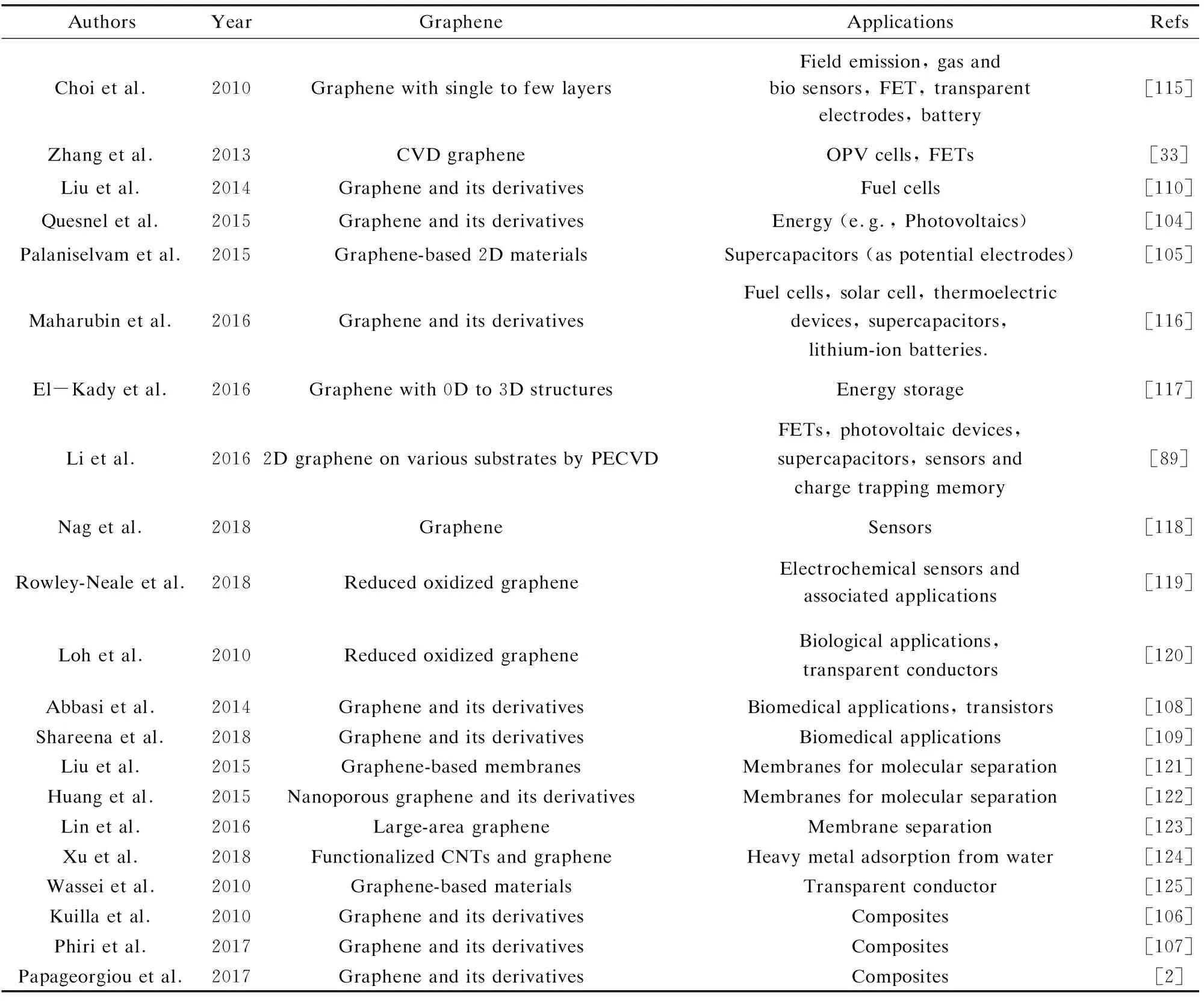
Table 2 Literatures on the applications of graphene-based materials
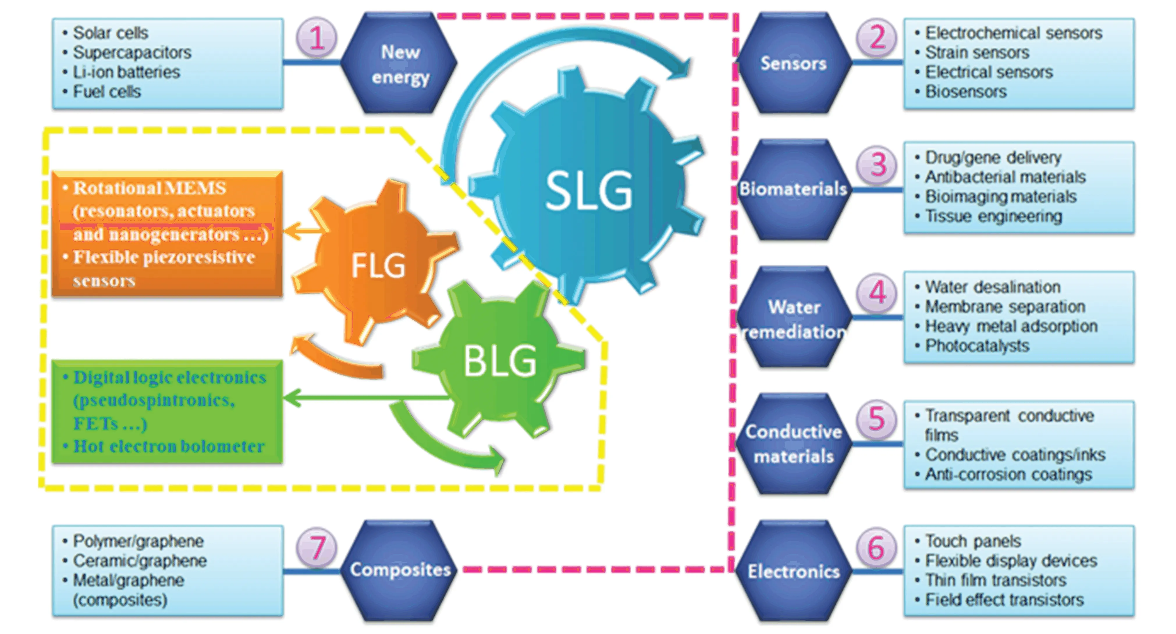
Fig.7 Potential applications of graphene
Secondly, as the simplest multilayer graphene, BLG shares not only the merits of SLG such as high electron mobility, mechanical strength and flexibility[129], but also those of other multilayer graphene, such as band-gap opening and coherent phonons, which leads to some unique and attractive potentials[17]. Here are some typical examples: 1) Owing to the tunable bandgap, BLG has exhibited many advantages, e.g., unique electrical characteristic of slowly increased conductivity with the increase of charge density, unipolar p-type MOSFET behavior and high on/off current-ratio (104- 107) at room temperature, in digital logic applications such as FETs, pseudo-spintronics and other electronics[130-131]. 2) BLG has tunable Fano resonance for the phonon mode in infrared spectra, which can be used as hot electron bolometer. It was reported that the BLG-based hot electron bolometer has much lower noise equivalent power and 3-5 orders of magnitude larger intrinsic speed, compared with the commercial silicon bolometer[129]. 3) BLG has exhibited similar effective Young’s modulus to that of SLG, but higher levels of reinforcement in nanocomposites according to the result of strain-induced Raman 2D-band shift. Notably, there was no slippage observed between the interlayers of BLG which was found for TLG and FLG and would lead to a decrease in the Young’s modulus of the composites[132]. Therefore, BLG, rather than SLG, may be the best choice for improving the mechanical properties of graphene-based nanocomposites.
Third, FLG has also received many interests from fundamental research to technological development: 1) The large structural anisotropy makes FLG a favorable candidate for the study of the rich physics from 3D to 2D systems[133]. 2) Compared with SLG and BLG, FLG has exhibited some unique advantages in the applications of solar cells and micro-electromechanical systems (MEMS)[134-138]. Li et al.[134]found that the power conversion efficiency of the solar cell fabricated with 4-layer graphene is two times larger than that with SLG. Besides, since the friction decreases monotonically as the layer-number of graphene increases (Fig. 1(d))[139], FLG demonstrates better wear resistance than SLG as tested in rotating MEMS which indicates a longer service life[140-141]. 3) FLG may exhibit better mechanical, thermal, and other properties under some circumstances[142-144]. For example, it was revealed that 7-layer CVD graphene may have higher thermal conductivity than graphene of 2-3 layers, due to the decrease of defects under higher growth temperature[142]. Liang et al.[143]found that for the graphene/polypropylene composites, FLG with 6-10 layers has better impact fracture toughness than that with 1-6 layers, since it can store more impact deformation energy. Moreover, in flexible piezoresistive sensors, FLG demonstrated better sensor sensitivity which rose from 0.051 to 11.1 kPa-1as the layer numbers of graphene increased from 4 to 14[144]. It can be predicted that the few-layer graphene with intrinsic and stable electrical conductivity and high dispersity in membrane-forming polymer solutions would be potentially used as vital additives in the highly sensitive sensing membranes for the fabrication of advanced long-life heavy-metal ion sensors[145-150].
In short, graphene with different layer numbers has exhibited respective advantages in both the physicochemical properties and potential applications. The preparation of high-quality graphene with well-controlled layer numbers will greatly enrich the commercial value and prospects.
5 Conclusions and Outlook
In summary, the status on a layer-number controllable synthesis of the graphenes based on the two complementary approaches of “top-down” and “bottom-up”, and the applications of the graphenes with different layer numbers have been elaborated. For “top-down” approaches, it is still of great challenge to prepare high-quality graphene with controlled layer numbers. However, some advances are quite enlightening:
1) Employing highly-diffusive supercritical CO2as dispersion media has demonstrated its improvement in layer-number controllability;
2) Thinning by laser or plasma are beneficial for the precise control of graphene layers.
For “bottom-up” approaches, the situation seems more optimistic:
1) Some effective techniques have been developed for precise control in the thickness of CVD graphene on metal substrates, such as introducing dual-metal substrates, layer-by-layer CVD, ion-implantation CVD;
2) Two-step plasma-enhanced CVD provides a good solution to the low-temperature growth of graphene on various substrates, especially dielectrics for application in electronics;
3) Template-assisted CVD (by layered-double-hydroxides) provides another option for the layer-number controllable CVD synthesis of graphene without transfer process;
4) In terms of thermal epitaxial growth, the introduction of graphite enclosure, which provides a relatively high partial-pressure of Si in dynamical balance, significantly enhances the controllability on its thickness and quality;
5) PMS-PVD should be paid more attention to and further explored, since it may be a low-cost and scalable solution for industrial production of high-quality graphene.
Although great challenges still exist in the scalable fabrication of high-quality graphene with controlled and homogeneous thickness, the above-reviewed significant progresses in the controllable preparation of graphene have shown us a brighter future. Considering the huge application potentials of graphene and the respective advantages of graphene with different layer numbers, more efforts should be devoted to the layer-number controllable preparation of high-quality graphene, as well as its feasibility of industrial production. We have every reason to believe that more and more achievements would be made in this field in the near future.
Acknowledgements
Xin-Gui Li and Mei-Rong Huang are grateful to Professor Hiroshi Imahori, Professor Tomokazu Umeyama, Professor Tomohiro Higashino, and Ms. Naoko Nishiyama at Department of Molecular Engineering, Kyoto University, Japan for their assistance.
 Journal of Harbin Institute of Technology(New Series)2020年3期
- Journal of Harbin Institute of Technology(New Series)的其它文章
- Evolution Toward Artificial Intelligence of Things Under 6G Ubiquitous-X
- Evaluation Method of Output Waveform Quality for Neutral-Point- Clamped Three-Level Converter
- Review: Scalable Fabrication of Polymeric Nanofibers from Nano- Spinning Techniques to Emerging Applications
- Controlled Movements in Superlubric MEMS
- Review: Recent Progress on Poly(ether ether ketone) and Its Composites for Biomedical, Machinery, Energy and Aerospace Applications
- Modified Adsorption Capacity to Space Molecular Pollutant of Zeolite via Interface Engineering with Atomic Layer Deposition