
Tunneling field effect transistors based on in-plane and vertical layered phosphorus heterostructures?
2017-08-30 08:26:30ShenyanFeng馮申艷QiaoxuanZhang張巧璇JieYang楊潔MingLei雷鳴andRugeQuhe屈賀如歌
Chinese Physics B 2017年9期
Shenyan Feng(馮申艷),Qiaoxuan Zhang(張巧璇),Jie Yang(楊潔),Ming Lei(雷鳴),and Ruge Quhe(屈賀如歌)
State Key Laboratory of Information Photonics and Optical Communications and School of Science, Beijing University of Posts and Telecommunications,Beijing 100876,China
Tunneling field effect transistors based on in-plane and vertical layered phosphorus heterostructures?
Shenyan Feng(馮申艷),Qiaoxuan Zhang(張巧璇),Jie Yang(楊潔),Ming Lei(雷鳴)?,and Ruge Quhe(屈賀如歌)?
State Key Laboratory of Information Photonics and Optical Communications and School of Science, Beijing University of Posts and Telecommunications,Beijing 100876,China
Tunneling field effect transistors(TFETs)based on two-dimensional materials are promising contenders to the traditional metal oxide semiconductor field effect transistor,mainly due to potential applications in low power devices.Here, we investigate the TFETs based on two different integration types:in-plane and vertical heterostructures composed of two kinds of layered phosphorous(β-P and δ-P)by ab initio quantum transport simulations.NDR effects have been observed in both in-plane and vertical heterostructures,and the effects become significant with the highest peak-to-valley ratio(PVR) when the intrinsic region length is near zero.Compared with the in-plane TFET based on β-P and δ-P,better performance with a higher on/off current ratio of~106 and a steeper subthreshold swing(SS)of~23 mV/dec is achieved in the vertical TFET.Such differences in the NDR effects,on/off current ratio and SS are attributed to the distinct interaction nature of the β-P and δ-P layers in the in-plane and vertical heterostructures.
tunneling field effect transistors,negative differential resistance effect,on/off current ratio,subthreshold swing
1.Introduction
The metal oxide semiconductor field effect transistor (MOSFET)is the basic building block of modern digital,analog,and memory circuits.However,the power consumption becomes a severe issue with the scaling down of the transistor.Tunneling field effect transistor(TFET)is based on the switching mechanism of band to band tunneling instead of thermionic emission as in the case of MOSFET.[1,2]Therefore,TFET does not suffer from the 60 mV/dec limit of the subthreshold swing(SS),rendering it promising forlow-power applications.
TFETs based on bulk semiconductors,such as Si and III–V materials,have been explored for TFETs.[3–7]Especially,the SS of sub-60 mV/dec has been realized in the fabricated Si[8,9]and GeSn quantum well p-channel TFETs.[10]Compared with the conventional bulk semiconductors with the presence of band-tail states,the two-dimensional(2D)semiconductors and related heterostructures with sharp band edges have shown promise to obtain sharp switching in 2D based TFETs.The fabricated 2D WSe2/SnSe2vertical heterostructure TFET achieves a SS of 100 mV/dec at room temperature over several orders of magnitude of drain current.[11]A record-low minimum SS of 3.9 mV/dec is realized in the atomically thin MoS2TFET at room temperature.[12]Theoretically,the 2D phosphorene TFETs are predicted to show SS below 60 mV/dec and a wide range of on-current depending on the transport direction due to the highly anisotropic nature of phosphorene.[13]
Besides the potential for low power applications,[14,15]another attractive feature of TFET is the possibility of a novel negative differential resistance(NDR)effect under forward bias voltage,which is caused by the quantum mechanical tunneling of electrons through an ultrathin barrier to provide high currentatlow voltage.[16]This NDR effect has a good prospect on high frequency switching oscillators and analog-to-digital converters.[17,18]
Recently,2D van der Waals(vdW)vertical heterostructures,such as graphene/BN/graphene,[19]MoS2/h BN/MoS2,[20]WSe2/SnSe2,[21]MoS2/WSe2,[22]and MoS2/MoSe2[23]have been used to fabricate TFETs.In these TFETs,it is a vdW interaction between the layers in the vertical heterostructures.Apart from the weak vdW interaction, heterostructures can be formed through the strong covalent interaction in the atomic interface between the two materials in the in-plane direction.While the current researches on 2D TFETs are mostly focused on those based on the vdW vertical heterostructures,there are few studies concerning the 2D in-plane TFETs,to the best of our knowledge.
The 2D layered phosphorus,which possesses a few stable structural phases,is attracting increasing attention recently. Among these phases,except for the commonly studied black phosphorus,few layered blue phosphorus(β-P),an in-planehexagonal isotropic structure,has also been successfully synthesized on Au(111).[24]TFET based on black phosphorushas been studied theoretically.[13]Unlike the isotropic β-P with a sizable band gap of around 2 eV,few layered δ-P is with a narrow band gap of 0.45 eV.[25]Beyond these phases mentioned above,other new monolayer(ML)phosphorus allotropes are also predicted based on ab initio calculations.[26]These different phosphorus phases could coexist by applying certain strain. The coexistence of different structural phases of layered phosphorus with fantastic properties enriches this material family and offers a novel platform for the next generation development of photoelectric devices.
In this paper,we investigate transport properties of the prototype p–i–n TFETs based on in-plane and vertical het-erostructures formed by semi-infinite β-P and δ-P layers via ab initio quantum transport simulations.Both the in-plane and vertical tunneling junctions of δ-P and β-P show a significant NDR effect.We discover that different integrations of heterostructures can affect the NDR effect.The PVR of in-plane heterostructures decreases with the increase of the intrinsic region length.However,this phenomenon is not found in vertical heterostructures.In addition,vertical TFET has a higher on/off current ratio of~106and a steeper SS of~23 mV/dec than the in-plane one,suggesting a greater probability to create an apparent switching effect and reduce operating voltage. Therefore,for heterostructures based on δ-P and β-P,the vertical heterostructure is more suitable for TFET than the in plane heterostructure,providing new prospects of the phase manipulated layered phosphorus for novel electronics.
2.Calculations methods
The electron transport properties are performed by using density functional theory(DFT)[27]coupled with the nonequilibrium Green’s function(NEGF)method,[28–30]as implemented in the ATK 2015 package.We use the generalized gradient approximation(GGA)in the form of the Perdew–Burke–Ernzerhof(PBE)functional for exchange and correlation potential.[31]To correctly account for the dispersion interaction,we apply the optimized exchange van der Waals functional B86E of the Becke(optB86b vdW)functional.[32]We employ the single-zeta-polarized(SZP)basis set during the device simulations.The k-points of the electrodes(channel) are set to 1×18×18(1×18×6)to make the separation of k-point near~0.01?A?1in the Brillouin zone,and the mesh cutoff is set to be 75 Hartree.The temperature is set to 300 K.
The current is calculated by using the Landauer–Buttiker formula[33,34]
where T(ε,Vbias)represents the energy and voltage-resolved transmission function,f is the Fermi–Dirac distribution function,andμL,R=Ef±Vbias/2 represent the chemical potentials of the left and right electrodes,respectively.To make sure of the accuracy of the calculations,we have performed test calculations with different exchange and correlation methods and basis sets.Consistent results by these methods are obtained, which suggests that our settings are reasonable(see Supplementary materials for details).
3.Results and discussion
To research the transport properties,two kinds of p–i–n junction models based on 5-nm in-plane and vertical heterostructure channels and semi-infinite δ-P and β-P electrodes have been simulated as shown in Fig.1.[35]After geometry optimization,the vdW distance of the vertical heterostructure between the β-P and δ-P layer is 2.98?A.The δ-P in the pregion and β-P in the n-region are heavily doped with the density of ρ(p)=ρ(n)=1×10²¹m?3,a reasonable doping concentration,which can be achieved for the real device fabrication.[36]The different lengths of the intrinsic region (L1=0?A,L2=11?A,and L3=19?A)are considered.
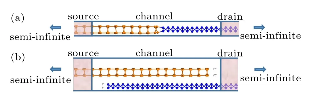
Fig.1.(color online)Heterostructures based on(a)in-plane and(b)vertical heterostructures.The source and drain are semi-infinite δ-P and β-P represented by blue arrows,respectively.The channel is composed of δ-P and β-P in-plane and vertical heterostructures,respectively.
We apply different bias voltages on in-plane and vertical heterostructures,respectively.The I–Vbiascurves with different lengths of the intrinsic region of in-plane and vertically stacked heterostructures are depicted in Fig.2.For in-plane heterostructures,significant NDR effects are observed in the output characteristic in Fig.2.The peaks and valleys of the current are located at around Vbias=0.25–0.30 V and 1.125–1.25 V,and the PVR values of the device with intrinsic region lengths of L1,L2,and L3are 59,49,and 11,respectively.The origin of the NDR effect is the change of band alignment between source and drain under different bias voltages,as shown in Fig.3.With heavily doped source and drain,the junction is of a broken type(type-III)band alignment under Vbias=0 V. The interband tunneling between source and drain dominates the current at a small bias voltage.At Vbias=0.25–0.30 V,the tunneling current reaches a peak.As the bias voltage becomes higher,the band alignment becomes type-II.The interband tunneling is unlikely to occur,and the current is dominated by thermionic injection of carriers.At Vbias=1.125–1.25 V,the current reaches a local minimum.The tunable type of band alignment by external voltage has also been demonstrated in the fabricated WSe2–MoS2heterostructures.[22]

Fig.2.(color online)(a1)and(a2)Two-probe models of the p–i–n junction composed of δ-P and β-P based on in-plane and vertically stacked heterostructures.The unit cells in gray and green shadows are heavily p-type and n-type doped,respectively.In these cases, the length of the intrinsic region is L1=0?A,L2=11?A,and L3=19?A.Yellow balls:δ-P;blue balls:β-P.(b1)and(b2)The I–V bias curves with different lengths of intrinsic region of in-plane heterostructures and vertically stacked heterostructures.
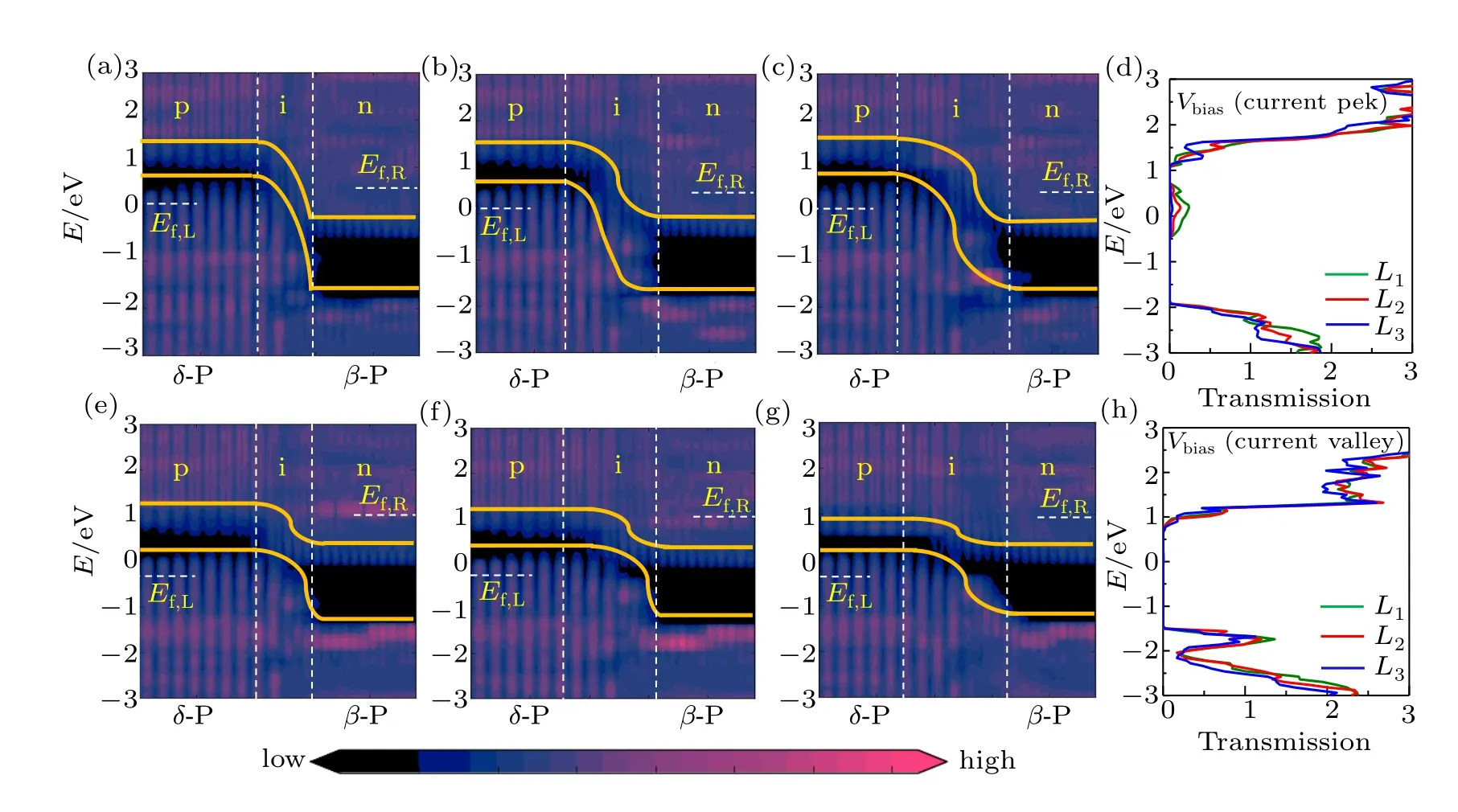
Fig.3.(color online)Spatial resolved LDOS and transmission spectra of the in-plane β/δ p–i–n junction at(a)–(d)current peak (V bias=0.25–0.30 V)and(e)–(h)valley(V bias=1.125 V),respectively.The lengths of the intrinsic regions are L1 in panels(a)and (e),L2 in panels(b)and(f),and L3 in panels(c)and(g),respectively.The Fermi levels of the left and right electrodes are denoted by E f,L and E f,R,respectively.
The NDR effect can also be understood by comparing the transmission spectra when the current reaches a peak and valley in Figs.3(d)and 3(h).Under Vbias=0.25–0.30 V (current peak),there are two gaps located in the range of 0.72 eV<E<1.08 eV and?1.86 eV<E<?0.48 eV,corresponding to the band gap of δ-P and β-P,respectively.Apparent transport humps are located between the gaps inside the bias window,contributing to the interband tunneling current.By contrast,the transmission possibility inside the bias window is almost zero under Vbias=1.125–1.25 V(current valley),suggesting a very low interband tunneling possibility. The decreasing PVR with the increase of the length of intrinsic region results from the thicker tunneling barrier in the intrinsic region and thus lower tunneling probability occurs at the current“valley”state.This trend is similar to that in the single-walled carbon nanotube and graphene nanoribbon p–n junction.[37–39]
For the vertical heterostructures of δ-P and β-P,we also observe significant NDR effects in the output characteristic in Fig.2.The peaks are located at around Vbias=0.5 V(L1= 0?A),0.375 V(L2=11?A),and 0.125 V(L3=19?A),whereas valleys of current are located at around Vbias=1.125–1.25 V. The PVR of the device with the intrinsic region lengths of L1, L2,and L3are 137,45,and 56,respectively.
The origin of the NDR effect vertical heterostructure is similar to that of in-plane heterostructuresas shown in Fig.4. Under Vbias=0 V,the junction is of broken type(type-III) band alignment resulting from the heavily doped source and drain as well.At a small bias voltage,the current is dominated by the interband tunneling between source and drain regions.At around Vbias=0.5 V,0.375 V,and 0.125 V,the tunneling current would reach a peak,then with a higher bias voltage,the band alignment transforms into type-II.There is low probability for achieving interband tunneling,and then the thermionic injection of carriers dominates the current.At around Vbias=1.125–1.25 V,the current would be a valley state.Comparing the transmission spectra in Figs.4(d)and 4(h),the phenomenon and principle of a vertical heterostructure are similar to those of an in-plane heterostructure.
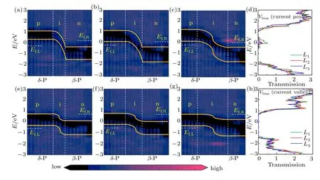
Fig.4.(color online)Spatial resolved LDOS and transmission spectra of the vertically stacked β/δ p–i–n junction at current peak (V bias=0.125–0.50 V)(a)–(d)and valley(V bias=1.125–1.25 V)(e)–(h),respectively.The lengths of the intrinsic regions are L1in panels(a)and(e),L2 in panels(b)and(f),and L3 in panels(c)and(g),respectively.The Fermi levels of the left and right electrodes are denoted by E f,L and E f,R,respectively.
For both in-plane and vertical heterostructures,the transmission eigenstates of the on-and off-state current and the kpoints Γ(0,0)are shown in Fig.5.In the upper panel,the transmission eigenstates can easily reach the drain(β-P)from the source region(δ-P),and the current reaches a peak.However,when the bias increases to~1.2 V,the carriers can hardly transport from the source to the drain region,and the current reaches a valley.
Comparing the NDR effect of in-plane and vertical heterostructures,we notice that the PVR value of the device with the intrinsic length of 0?A is the maximum value in both inplane and vertical heterostructures compared to the other two cases(L2=11?A and L3=19?A),resulting from the narrow intrinsic region.For the vertical heterostructures,PVR of the device with intrinsic lengths of 0?A and 19?A are 137 and 56,respectively,which are higher than those of in-plane heterostructures(59 and 11).However,PVR of the device with the intrinsic region length of 11?A is 45,which is similar to that of in-plane heterostructure(49).
The PVR is determined by the peak current and the valley current.When the intrinsic region length decreases,the peak current and valley current also decrease in both in-plane and vertical heterostructures.When the intrinsic region lengths are 0?A and 19?A,the PVRs of vertical heterostructures are higher than those of in-plane ones,because the valley current is similar but the peak currents of the vertical heterostructure are about 4.3 and 4.9 times larger than those of the in-plane heterostructure,respectively.However,when the intrinsic region length is 11?A,the peak current and valley current of the vertical heterostructure are both around 3 times larger than those of the in-plane heterostructure,so the PVR of in-plane and vertical heterostructures are similar.That is because the valley current of the in-plane heterostructure decreases rapidly from 0?A to 11?A relative to the vertical one.We can analyse this phenomenon from the transmission spectrum and LDOS.In the transmission spectrum in Fig.6,there are humps inside the bias window.Compared with transmission humps,we find that hump widths are almost the same,but the hump height of L2=11?A is one-third of that of L1=0?A,resulting in a great decrease in the valley current from 0?A to 11?A.The decrease of the transmission hump height is related to the existence of the interface states.In the in-plane heterostructure,the carriers could transport through the interface states from the left to the right electrodes,increasing the transmission possibility. Comparing the spatial resolved LDOS with L=0?A and 11?A, less interface states inside the gap of the intrinsic region of in-plane heterostructure are found when the intrinsic length is 11?A.Therefore,the transmission possibility from the left to the right electrodes decreases significantly when Liincreases from 0 to 11?A.
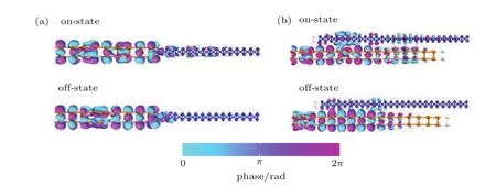
Fig.5.(color online)Transmission eigenstate of the current peak and current valley states of the(a)in-plane and(b)vertical heterostructures.Yellow balls:δ-P;blue balls:β-P.
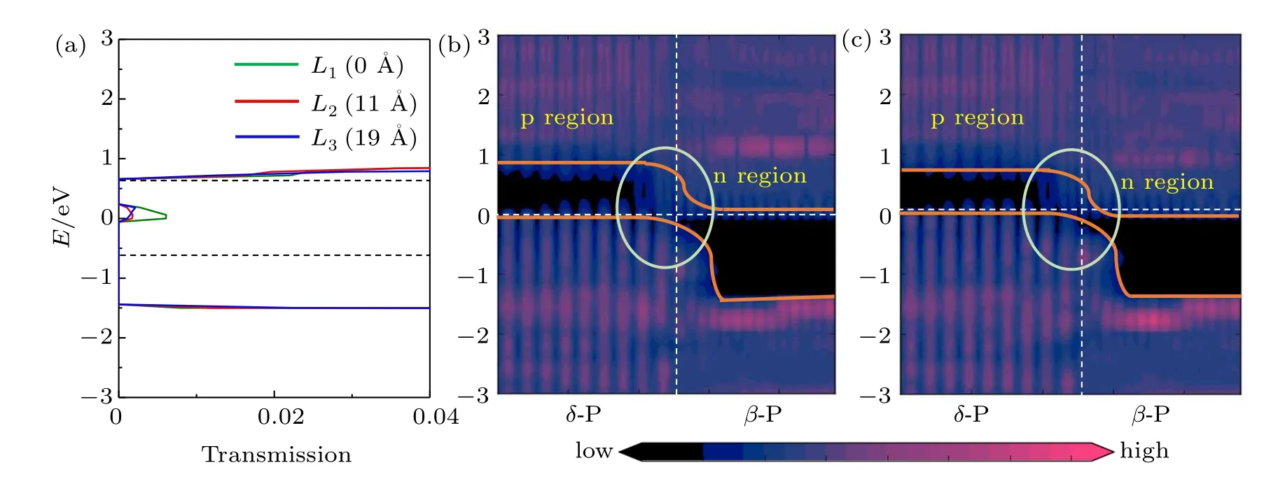
Fig.6.(color online)(a)Transmission spectra and spatial resolved LDOS of the in-plane β/δ p–i–n junction current peak valley (V bias=1.125–1.25 V),respectively.The black dash line represents the bias window.The lengths of the intrinsic regions are L1=0?A in panel(b)and L2=11?A in panel(c),respectively.The Fermi levels of the left and right electrodes are denoted by E f,L and E f,R, respectively.
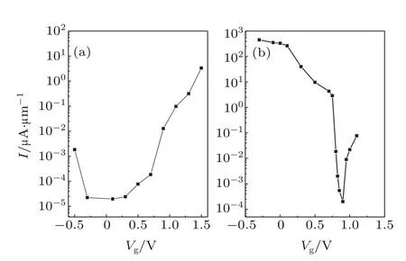
Fig.7.Transfer characteristics of(a)in-plane and(b)vertically stacked TFETs at V bias=0.1 V.
Because of the inefficient gate control and severe short channel effects with the short channel of 5 nm,we further study a long channel TFET(L=16 nm).The intrinsic region length is 13 nm in this device.The Ids–Vgcurves of in-plane and vertical TFETs are shown in Fig.7.
For in-plane TFET,the off-state current,which is read at the state where the minimum current appears,is 2.0× 10?5μA/μm.Within a supply voltage Vdd=1.2 V,the onstate is~3μA/μm and the on/off current ratio is 1.6×10⁵. The steepest SS value is 108 mV/dec.Compared with the in-plane one,the vertical TFET shows better performance in both on/off current ratio and SS value.Within a 1.2 V supply voltage,the on/off current ratio of the vertical TFET is about 2.2×10⁶,one order of magnitude greater than that of the inplane one.The steepest SS value is only 23 mV/dec,indicating a much stronger gate control ability in the vertical TFET than that in the in-plane one.Therefore,in terms of the higher on/off current ratio and lower SS value,the vertical TFET has a greater probability to create an apparent switching effect and reduce the operate voltage than the in-plane one.
The reason for the more significant NDR effect,the higher on/off current ratio and steeper SS in the vertical heterostructure than in the in-plane one might be their distinct nature of the interaction between the two materials in the heterostructures.In the vertical heterostructure,the β-P and δ-P are connected by the vdW interaction along the vertical direction.Interlayer vdW interaction will not induce structural disorder and scattering center that affects the charge transport in the vertical heterostructure.[40–42]However,in the in-plane heterostructure,the β-P and δ-P layers are connected by the strong covalent bonds,and a grain boundary forms between the two materials.As shown in Fig.8,there are some localized interface states as shown in the ellipse circle and the energy of interface states is in a range from 0.4 eV to 0.6 eV inside the band gap of β-P.Like the metal induced gap states in the metal-semiconductor heterojunction,the interface states could serve as a reservoir for holes or electrons.The interface states can become the sources of Coulomb scattering when they are charged.[43]Therefore,the existence of interface states in the in-plane heterostructure could lead to the mobility degradation and the electrical conductivity reduction.[44–47]

Fig.8.(color online)Spatial resolved LDOS of in-plane heterostructures without doping.The Fermi level is set to zero.
4.Conclusions
In summary,we show apparent NDR effects in p–i–n tunneling junction based on β-P and δ-P heterostructures.The PVR value is the highest when the intrinsic region length becomes zero in both in-plane and vertical tunneling junctions. For the vertical heterostructures,the PVRs of the device with intrinsic region lengthsof0?Aand 19?Aare 137 and 56,respectively,which are higher than those in the case of the in-plane heterostructures(59 and 11).However,the PVR of the device with an intrinsic region length of 11?A is 45,which is similar to that of in-plane heterostructure(49).Moreover,the 16-nm channel vertical TFET exhibits a high on/off current ratio of~106and a steep SS of~23 mV/dec,which has better performances than in-plane TFET based on β-P and δ-P.These outstanding performances in the TFET based on the vertical heterostructure are related to the relatively high electrical conductivity as the interlayer vdW interaction without inducing a scattering center,in contrast with the formation of the grain boundary in the in-plane heterostructures.
[1]Avci U E,Rios R,Kuhn K and Young I A 2011 Symposium on VLSI Technology-Digest of Technical Papers 124
[2]Wang Y,Jiao W L,Hu H F,Liu Y T and Cao F 2012 Chin.Phys.B 21 056104
[3]Tomioka K,Yoshimura M and Fukui T 2012 Symposium on VLSI Technology,June 12–14,2012,Honolulu,HI,USA,p.12879740
[4]Liu M,Liu Y,Wang H,Zhang Q,Zhang C,Hu S,Hao Y and Han G 2015 IEEE Trans.Electron Devices 62 1262
[5]Wang H,Han G,Liu Y,Hu S,Zhang C,Zhang J and Hao Y 2016 IEEE Trans.Electron Devices 63 303
[6]Pandey R,Schulte-Braucks C,Sajjad R N,Barth M,Ghosh R K, Grisafe B,Sharma P,von den Driesch N,Vohra A,Rayner B,Loo R, Mantl S,Buca D,Yeh C C,Wu C H,Tsai W,Antoniadis D and Datta S 2016 IEEE International Electron Devices Meeting(IEDM),December 3–7,2016,San Francisco,CA,USA,p.16651056
[7]Wang Y,Han G,Liu Y,Zhang C,Feng Q,Zhang J and Hao Y 2017 IEEE Trans.Electron Devices 64 1541
[8]Huang Q,Huang R,Zhan Z,Qiu Y,Jiang W,Wu C and Wang Y 2012 IEEE International Electron Devices Meeting,December 10–13,2012, San Francisco,CA,USA,p.13384027
[9]Jeon K,Loh W Y,Patel P,Kang C Y,Oh J,Bowonder A,Park C,Park C S,Smith C,Majhi P,Tseng H H,Jammy R,Liu T J K and Hu C 2010 Symposium on VLSI Technology,June 15–17,2010,Honolulu, HI,USA,p.11488276
[10]Han G,Wang Y,Liu Y,Zhang C,Feng Q,Liu M,Zhao S,Cheng B, Zhang J and Hao Y 2016 IEEE Electron Device Lett.37 701
[11]Roy T,Tosun M,Hettick M,Ahn G H,Hu C and Javey A 2016 Appl. Phys.Lett.108 083111
[12]Sarkar D,Xie X,Liu W,Cao W,Kang J,Gong Y,Kraemer S,Ajayan P M and Banerjee K 2015 Nature 526 91
[13]Chang J and Hobbs C 2015 Appl.Phys.Lett.106 083509
[14]Ionescu A M and Riel H 2011 Nature 479 329
[15]Seabaugh A C and Zhang Q 2010 Proc.IEEE 98 2095
[16]Zhao Y,Wan Z,Xu X,Patil S R,Hetmaniuk U and Anantram M P 2015 Sci.Rep.5 10712
[17]Brown E R 1991 Appl.Phys.Lett.58 2291
[18]Broekaert T P E,Brar B,van der Wagt J P A,Seabaugh A C,Morris F J,Moise T S,Beam E A and Frazier G A 1998 IEEE J.Solid-State Circ.33 1342
[19]Britnell L,Gorbachev R V,Jalil R,Belle B D,Schedin F,Mishchenko A,Georgiou T,Katsnelson M I,Eaves L,Morozov S V,Peres N M R, Leist J,Geim A K,Novoselov K S and Ponomarenko L A 2012 Science 335 947
[20]Srivastava A and Fahad M S 2016 Solid-State Electron.126 96
[21]Li M O,Esseni D,Nahas J J,Jena D and Xing H G 2015 IEEE J. Electron Devices Soc.3 200
[22]Roy T,Tosun M,Cao X,Fang H,Lien D H,Zhao P,Chen Y Z,Chueh Y L,Guo J and Javey A 2015 ACS Nano 9 2071
[23]Lu S C,Mohamed M and Zhu W 2016 2D Mater.3 011010
[24]Zhang J L,Zhao S,Han C,Wang Z,Zhong S,Sun S,Guo R,Zhou X, Gu C D,Yuan K D,Li Z and Chen W 2016 Nano Lett.16 4903
[25]Guan J,Zhu Z and Tománek D 2014 Phys.Rev.Lett.113 046804
[26]Wu M,Fu H,Zhou L,Yao K and Zeng X C 2015 Nano Lett.15 3557
[27]Fuchs M and Scheffler M 1999 Comput.Phys.Commun.119 67
[28]Lake R,Klimeck G,Bowen R C and Jovanovic D 1997 J.Appl.Phys. 81 7845
[29]Brandbyge M,Mozos J L,Ordejón P,Taylor J and Stokbro K 2002 Phys.Rev.B 65 165401
[30]Taylor J,Guo H and Wang J 2001 Phys.Rev.B 63 245407
[31]Perdew J P,Burke K and Ernzerhof M 1996 Phys.Rev.Lett.77 3865
[32]Klime?s J,Bowler D R and Michaelides A 2011 Phys.Rev.B 83 195131
[33]Büttiker M,Imry Y,Landauer R and Pinhas S 1985 Phys.Rev.B 31 6207
[34]Datta S 1995 Electronic Transport in Mesoscopic Systems(Cambridge: Cambridge University Press)p.70
[35]Li Y C,Zhang H M,Zhang Y M,Hu H Y,Wang B,Lou Y L and Zhou C Y 2013 Chin.Phys.B 22 038501
[36]Fang H,Chuang S,Chang T C,Takei K,Takahashi T and Javey A 2012 Nano Lett.12 3788
[37]Li Z,Zheng J,Ni Z,Quhe R,Wang Y,Gao Z and Lu J 2013 Nanoscale 5 6999
[38]Ren H,Li Q X,Luo Y and Yang J 2009 Appl.Phys.Lett.94 173110
[39]Nguyen V H,Bournel A and Dollfus P 2011 J.Appl.Phys.109 093706
[40]Lee C H,Schiros T,Santos E J G,Kim B,Yager K G,Kang S J,Lee S,Yu J,Watanabe K,Taniguchi T,Hone J,Kaxiras E,Nuckolls C and Kim P 2014 Adv.Mater.26 2812
[41]Lin Y C,Li J,de la Barrera S C,Eichfeld S M,Nie Y,Addou R, Mende P C,Wallace R M,Cho K,Feenstra R M and Robinson J A 2016 Nanoscale 8 8947
[42]Doan M H,Jin Y,Adhikari S,Lee S,Zhao J,Lim S C and Lee Y H 2017 ACS Nano 11 3832
[43]Friedrichs P,Kimoto T,Ley L and Pensl G 2011 Silicon Carbide (WILEY-VCH Verlag GmbHamp;Co.KGaA,Weinheim)
[44]Tsen A W,Brown L,Levendorf M P,Ghahari F,Huang P Y,Havener R W,Ruiz-Vargas C S,Muller D A,Kim P and Park J 2012 Science 336 1143
[45]Mesaros A,Papanikolaou S,Flipse C F J,Sadri D and Zaanen J 2010 Phys.Rev.B 82 205119
[46]Peres N M R,Guinea F and Castro N A H 2006 Phys.Rev.B 73 125411
[47]Hua T,Xu W W,Ji Z M,Guo D Y,Wang Q Y,Ma X R and Liang R Y 2016 Chin.Phys.B 25 067401
7 April 2017;revised manuscript
24 May 2017;published online 27 July 2017)
10.1088/1674-1056/26/9/097401
?Project supported by the National Natural Science Foundation of China(Grant Nos.11604019,61574020,and 61376018),the Ministry of Science and Technology of China(Grant No.2016YFA0301300),the Fund of State Key Laboratory of Information Photonics and Optical Communications(Beijing University of Posts and Telecommunications),China,and the Fundamental Research Funds for the Central Universities,China(Grant No.2016RCGD22).
?Corresponding author.E-mail:mlei@bupt.edu.cn
?Corresponding author.E-mail:quheruge@bupt.edu.cn
?2017 Chinese Physical Society and IOP Publishing Ltd http://iopscience.iop.org/cpb http://cpb.iphy.ac.cn
猜你喜歡
新作文·小學(xué)低年級版(2022年5期)2022-08-30 02:42:42
科學(xué)家(2022年5期)2022-05-13 21:42:18
家教世界·創(chuàng)新閱讀(2022年3期)2022-04-12 23:48:22
Chinese Physics B(2022年4期)2022-04-12 03:47:22
Chinese Physics B(2019年7期)2019-08-06 02:07:02
中學(xué)課程輔導(dǎo)·教學(xué)研究(2018年35期)2018-04-07 14:28:14
家庭影院技術(shù)(2017年8期)2017-10-13 08:19:16
商情(2017年5期)2017-03-30 23:58:25
瘋狂英語·新悅讀(2017年12期)2017-02-18 02:34:25
詩歌月刊(2016年10期)2016-12-16 00:51:50

- Chinese Physics B的其它文章
- Relationship measurement between ac-Stark shift of 40Ca+clock transition and laser polarization direction?
- Air breakdown induced by the microwave with two mutually orthogonal and heterophase electric field components?
- Collective motion of active particles in environmental noise?
- Temperature dependence of heat conduction coefficient in nanotube/nanowire networks?
- Analysis of dynamic features in intersecting pedestrian flows?
- Heat transfer enhancement in MOSFET mounted on different FR4 substrates by thermal transient measurement?