
Ionization wave propagation and cathode sheath formation due to surface dielectricbarrier discharge sustained in pulsed mode
2023-11-19 13:32:38KonstantinosGIOTISPanagiotisSVARNASEleftheriosAMANATIDESKristaqGAZELIGuillaumeLOMBARDIandPolykarposPAPADOPOULOS
Plasma Science and Technology 2023年11期
Konstantinos GIOTIS ,Panagiotis SVARNAS ,Eleftherios AMANATIDES ,Kristaq GAZELI ,Guillaume LOMBARDI and Polykarpos K PAPADOPOULOS
1 High Voltage Laboratory(Plasma Technology Room),Department of Electrical and Computer Engineering,University of Patras,Rion Patras 26504,Greece
2 Laboratoire des Sciences des Procédés et des Matériaux(LSPM-CNRS),Université Sorbonne Paris Nord,Villetaneuse F-93430,France
3 Plasma Technology Laboratory,Department of Chemical Engineering,University of Patras,Rion Patras 26504,Greece
4 Department of Mechanical Engineering and Aeronautics,University of Patras,Rion Patras 26504,Greece
Abstract This work deals with the experimental study of a surface dielectric-barrier discharge,as a part of the ongoing interest in the control of plasma induced electro-fluid dynamic effects(e.g.plasma actuators).The discharge is generated using a plasma reactor consisting of a fused silica plate which is sandwiched between two printed circuit boards where the electrodes are developed.The reactor is driven by narrow high voltage square pulses of asymmetric rising(25 ns)and falling(2.5 μs)parts,while the discharge evolution is considered in a temporarily and spatially resolved manner over these pulses.That is,conventional electrical and optical emission analyzes are combined with high resolution optical emission spectroscopy and ns-resolved imaging,unveiling main characteristics of the discharge with a special focus on its propagation along the dielectric-barrier surface.The voltage rising part leads to cathode-directed ionization waves,which propagate with a speed up to 105 m s-1.The voltage falling part leads to cathode sheath formation on the driven electrode.Τhe polarization of the dielectric barrier appears critical for the discharge dynamics.
Keywords: atmospheric pressure plasma,surface DBD,streamer,UV-NIR optical emission spectroscopy,ICCD fast imaging
1.Introduction
Dielectric-barrier discharges (DBDs) are nonequilibrium electrical discharges with electrode configurations containing one or more insulating layers in the current path to prevent arcing between the electrodes.Furthermore,the related setups are attractive due to the simplicity of their technical design and its implementation [1].DBDs may be divided into two broad categories,for commonly used configurations: (i) volume discharges [2-5] and (ii) surface discharges [3-5].In the volume discharge case,any physical path between the two conductive electrodes necessarily includes both the dielectric barrier and the gas medium.The associated discharge regimes and ionization waves have been investigated extensively for systems like plasma jets[6-11],packed beds[12-14],etc[15,16].In the surface discharge case,there is at least one path along which the two electrodes may be reached through the dielectric barrier only.This concept attracts interest for a large variety of fields,including medicine [17-21],material processing [22-24],flow field control(plasma actuators)[25-27],aerodynamic propulsion[28-31],assisted combustion[32-35],icing control[36-38],ozone generation[39-42],environment[43-45],and agriculture[46,47],just to name a few.
Consequently,extended research has been devoted to the physical mechanisms governing surface DBDs (SDBDs).In analogy with the traditional sliding discharges [48],the high voltage applied to the driven electrode leads to an electric field enhanced in the electrode vicinity.This field induces ionization through electron collisions osculating the dielectric barrier.At the same time,currents normal to the latter,charge the capacitance formed between the grounded electrode and the plasma.The fields due to the surface charges and the space charges account for the local electric field which resembles to a solitary wave.In the case of sliding discharges which expand along a plane,the ionization at the front of the wave is related to the transverse electric field [48].The geometry of the setup determines the propagation of the peaks of both the longitudinal and the transverse electric field along the dielectric surface.
In addition,the dynamics of the SDBDs and the kinetics of the generated plasmas are closely related to the driving voltage waveform.Therefore,SDBDs may be broadly categorized in alternating current (AC) and nanosecond pulsed (ns-pulsed)ones.In the ‘AC’case,during the positive voltage circle,the discharge is exhibited with numerous erratic high current impulses superposed on a permanent lower current component at the driving frequency.These impulses are related with the development of a positive ion cloud over the surface,but its development is interrupted by steamer breakdown and restarts from zero after each streamer pulse.The negative part of the cycle is composed of a much larger number of current pulses(frequency in the MHz range)of smaller amplitudes[49].On the other hand,in the ‘ns-pulsed’ case,when the air-exposed electrode plays the role of the anode,the discharge is exhibited with a unified current impulse coinciding with the voltage positive(steep)slope.During this phase,streamer propagation takes place along the dielectric-barrier surface.Then,at the falling(steep)part of the voltage pulse,the potential difference between the charged dielectric-barrier surface and the exposed electrode quickly increases to values over the breakdown voltage,and a second current impulse is initiated.During this phase,the exposed electrode plays the role of the cathode,and a cathode sheath is formed over it[50].
In a rigorous interpretation,SDBDs involve thermal,electrostatic,electro-hydrodynamic,and magneto-hydrodynamic effects,that lead to surface ionization waves,charge transport,accumulation,and dissipation on the dielectric barrier,discharge contraction,and different types of flow perturbations.The latter include low-speed near-surface jets,spanwise and streamwise vortices,weak shock waves,and near-surface localized stochastic perturbations.These matters are ably considered in topical reviews[3,4,51].
Concerning the relevant research,the understanding of fundamental processes is the outcome of several experiments that have been conducted for the investigation of the temporal and spatial evolution of the SDBDs.Specifically,the dynamic surface charge distribution has been calculated by measuring the electrical potential profile through the Pockels effect[52]or an electrostatic probe [53-55].These measurements indicate that the charge accumulation and release depend on the applied voltage waveform and the dielectric-barrier properties.In addition,it is shown that there is remaining charge per period on the dielectric-barrier surface which affects the discharge propagation and features.The time-resolved electric field has also been mapped on the dielectric-barrier surface directly,using electric field induced second harmonic(E-FISH)[55,56]and optical emission spectroscopy (OES) [57,58] as main diagnostic methods.The electric field near the high voltage electrode was found to be a superposition of the Laplacian field and the field due to the residual surface charge until the breakdown happens,and then the electric field decreases to a minimum value[55].Surface ionization wave propagation has been recorded too,elaborately,with the use of intensified charge-coupled device (ICCD) imaging for different SDBD setups and operational windows,such as various electrode geometries [59-61],dielectric materials [55,62],voltage waveforms[56,63-66],ratios of N2to O2gases[67,68],and environmental conditions [69].Eventually,endurance tests have been carried out,revealing aging and deterioration of the materials involved in the setups[70-73].
Meanwhile,numerous simulations have contributed to the field,either exploiting or completing the experimental results.The simulations consider the electro-hydrodynamic force and the aerodynamic flow acceleration [74],the relative contribution of the positive and negative ions in the momentum transfer[49],the momentum and the thermal transfer[50],the electro-hydrodynamic force and the power consumption[75],various chemical reactions [76-78],the Joule heating,the periodic electrostatic force,and the Lorentz acceleration[79],the photoionization [80],the periodically observed current pulses [81],the surface charges [82],the dielectric barrier configuration [83],etc.Besides,analytical models have derived equations for fundamental quantities[84].
This work presents the implementation of a particular SDBD reactor and the relative investigation under pulsed operation.The applied voltage waveform refers to square pulses having fast rise(about 25 ns)and slow fall(about 2.5 μs)time,while the amplitude,the frequency,and the pulse width are adjustable.A fused quartz sheet is selected as the dielectric barrier and the electrodes are developed on printed circuit boards(PCBs).Electrical and optical techniques are applied to probe principal features of the discharge.Power consumption is measured as a function of the amplitude,the frequency,and the width of the high voltage pulses;values lower than 3 W are found.Simplified aging tests are also considered.High resolution OES is conducted for the identification of main emissive species,the record of specific molecules’ rotational distributions,and the evaluation of the vibrational and the rotational temperatures.They are found to be around 3100 K and 310 K,respectively.ICCD fast imaging is combined with photoelectron multiplier tube signals and unveils the propagation of distinct ionization waves during the voltage positive slope.The instantaneous propagation speed is evaluated,and it is found to be on the order of 105m s-1.The negative slope of the voltage provokes cathode sheath formation on the driven electrode.Finally,the crucial role of the dielectric barrier polarization is discussed.
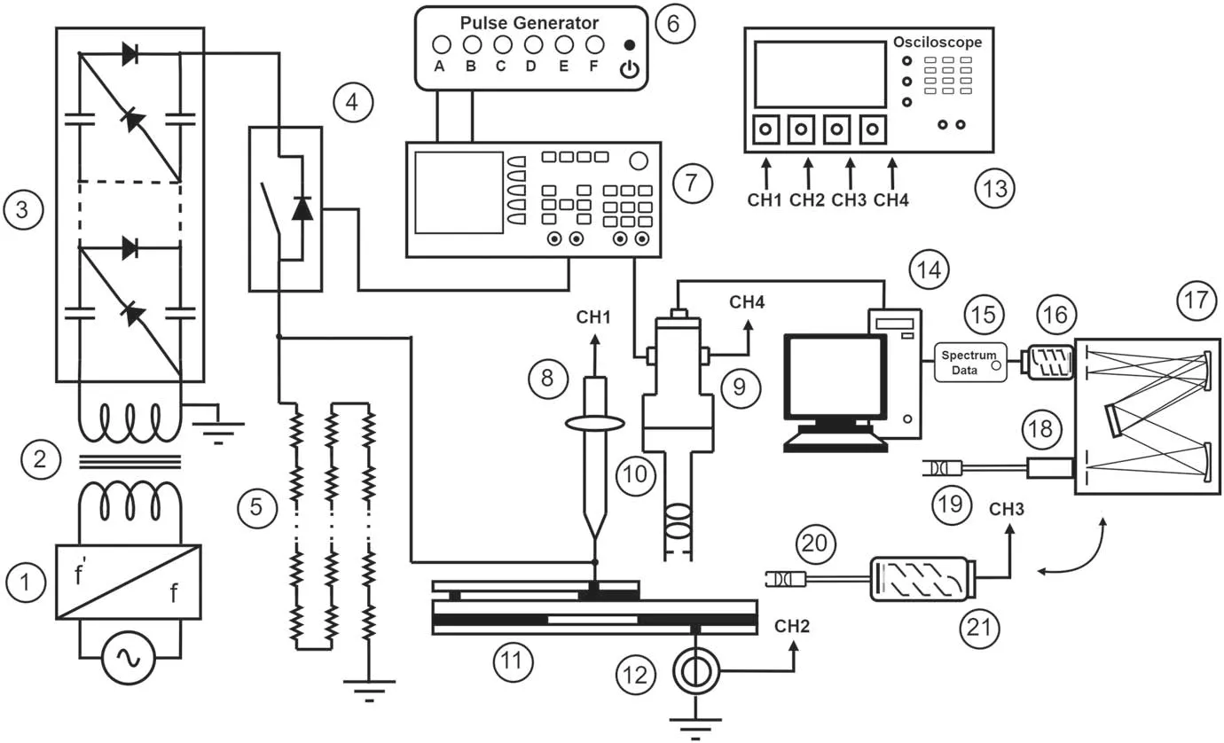
Figure 1.Conceptual diagram of the experimental setup.1:frequency-to-frequency converter;2:low voltage,isolation transformer;3:23-stage Cockcroft-Walton generator;4:high voltage MOSFET;5:pull-down resistor stack;6:6-channel pulse/delay generator;7:2-channel arbitrary waveform generator;(8):high voltage probe;(9):ICCD camera;(10):focusing system;11:plasma reactor;12:current transformer;13:oscilloscope;14:personal computer;15:data acquisition unit;16:1st PMT;17:monochromator;18:optical matcher;19:1st optical fiber with collimator;20:2nd optical fiber with collimator and pin hole;21:2nd PMT.The components 15-19,20 and 21 are interchanged.
2.Experimental setup
Figure 1 shows the block diagram of the setup used.The design of the plasma reactor is shown in figure 2.The reactor follows a DBD configuration,with the dielectric barrier to be a fused silica plate of 2 mm in thickness,provided by UQG Optics Ltd The patterns of the electrodes are developed on printed circuit boards (PCBs),having dielectric thickness of 960 μm and copper thickness of 18 μm (provided by LPKF Laser &Electronics).
The anode termination(figure 2(a):detail 1a and inset)is an array of line-to-circle parallel branches developed on the upper PCB,while the copper surface touches the quartz.The cathode is a simple rectangular strip developed on the lower PCB,while the copper surface touches the quartz(detail 3a in figures 2(a) and (b)).The copper patterns 1c and 3c in figures 2(a)and(b)serve as spacers maintaining the two PCBs and the quartz plane as parallel as possible;otherwise,the PCBs would be slightly tilted due to the copper thickness(18 μm).Thus,obviously,cathode is not encapsulated in the dielectric barrier.The PCB-quartz-PCB layers are sandwiched tightly by plastic bolts (see figure 7(a) below).The photo in figure 2(c)depicts the visible pattern of the plasma generated due to this SDBD configuration.
The driving voltage is generated by a pulsed high voltage power supply described in detail previously[85](conceptualized and designed by PlasmaHTec?;plasmahtec.com).Briefly,it consists of a Cockcroft-Walton cascade voltage multiplier and a solid-state switch connected in‘push mode’.This special design leads to high voltage square pulses of ns-rising edge and μsfalling edge,ascribing to the corresponding discharges discrete indented features(see section 3,and[85]).The output pulses,v(t),are permanently monitored with a high voltage passive probe(Tektronix;P6015;DC-75 MHz).Hereafter,the voltage amplitude is defined as the voltage value of the pulse plateau at the time point corresponding to the middle of its width.By this way,any overshoot,oscillations,plateau slope,etc,are discounted.The DBD current,i(t),is monitored with a current transformer(Pearson Electronics;6585;400 Hz-200 MHz).The wavelength-and space-integrated plasma emission is captured with a focusing probe(Newport;77646;fused silica)attached to a liquid light guide (Newport;77556;UV-visible) and observed over time with a photomultiplier (PMT;Hamamatsu R928;185-900 nm).A pin hole diaphragm(?0.5 mm)is placed in front of the focusing probe to prevent PMT photocathode saturation.The above signals are observed simultaneously on an oscilloscope (LeCroy;WaveRunner 44Xi-A;400 MHz;5 GSamples s-1per channel).
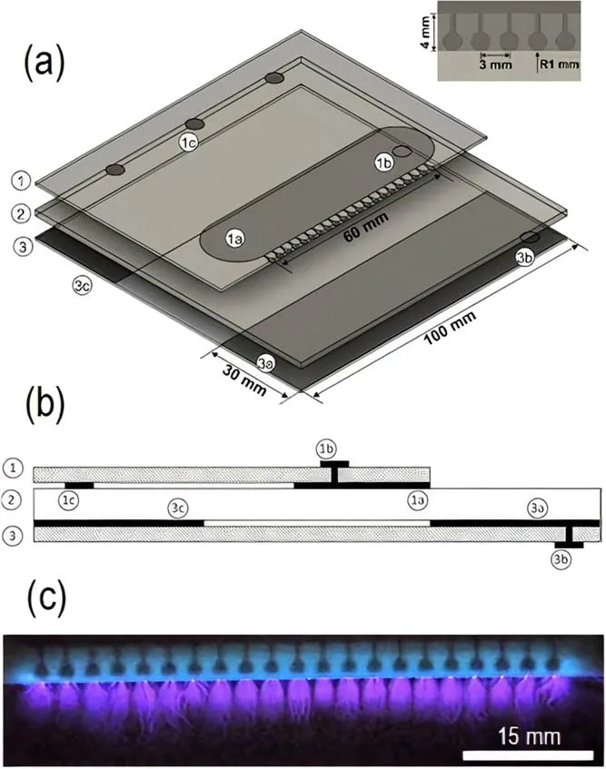
Figure 2.(a)Design of the plasma actuator(scaled).1:PCB with the high voltage electrode developed underneath(detail 1a and right-top inset);detail 1b:galvanized via-high voltage terminal;detail 1c:copper dots developed underneath-spacers.2:fused silica plate;3:PCB with the grounded electrode developed on the upper surface(detail 3a);detail 3b:galvanized via-ground terminal;detail 3c:copper stripe developed on the upper surface-spacer.(b)Cross section of the plasma actuator(not scaled).For the numbered parts refer to frame(a).(c)Conventional photo of the plasma induced by the surface DBD.Compare with the anode design in the inset of figure 2(a).Operating conditions:12 kV;2 kHz;pulse width 2 μs.
The above signals are corrected in terms of shifting in time.This is associated with(i)the coaxial cables,(ii)the head of the high voltage probe,(iii)the transit and anode rise times of the PMT,and (iv) the latency of the liquid light guide.The 1.5 ns useable rise time of the current transformer is ignored.Furthermore,due to the ns-rising part of the high voltage pulse,background noise is induced and disturbs the PMT signals.This background is recorded by masking the PMT and is then subtracted from the raw signal.The μs-falling part of the high voltage pulse does not arise such an issue.
The mean DBD power is evaluated using the integral×i(t)dt,where T stands for the pulse period and Δt for a fraction of the period corresponding to an interval around the pulse plateau.The signalsv(t) andi(t) are averaged(100 samples) and the sampling rate is 5 GSamples s-1per channel.
The time-and space-integrated light is collected and guided by an optical fiber (CeramOptec GmbH;UV 1500/1590 N;NA 0.22)to a high-resolution monochromator(Jobin Yvon;THR 1000;170-750 nm;2400 grooves mm-1)and the radiative species in the optical emission spectrum are thus identified.In this case,a fused silica collimating lens(?6 mm;8.7 mm confocal length;200-2500 nm) is used without any diaphragm,while an optical matcher is installed on the entrance slit of the instrument for optimal alignment of the fiber image.Hg(Ar)(Newport;6035)and QTH(Newport;6334NS;250 W)lamps are used for wavelength and relative spectral efficiency calibration,respectively.Rotational temperature of probe molecules is assessed using a custom software[86].
In addition,a portable spectrometer of lower resolution(AvaSpec;ULS4096CL-EVO-UA-10)is employed to explore wider wavelength ranges.It is equipped with a 300 grooves mm-1grating (200-1100 nm;blaze 300 nm) and a CMOS photodetector (4096 pixels).The light is efficiently led to the unit by means of the abovementioned collimating lens and a fused silica optical fiber(200-2500 nm;NA 0.22).Calibration of this optical assembly is carried out similarly to the monochromator case.
Discharge dynamics is visualized by means of fast imaging.An ICCD camera (Andor;iStar DH734-18F-03;180-850 nm;photocathode gating rate up to 50 kHz;minimum optical gate width 1.2 ns;active pixels 1024×1024) is employed.Two bi-convex lenses (ThorLabs,Inc.;LB941;UV fused silica) are mounted back-to-back and housed in a dark tube(detail 10 in figure 1)which is attached on the camera front flange.The back-to-back lenses are adjusted at a distance equal to two times the combined focal length both from the camera sensor and the reactor barrier(quartz surface)and are in contact with an optical aperture(?16 mm).This concept leads to 1:1 magnification of the plasma emissive pattern and corrects lens aberrations to an appreciable extent.
ICCD snapshots are captured along the high voltage pulses.A multichannel pulse/delay generator (Berkley Nucleonics Corp;Model 525;resolution 4 ns;rms jitter <50 ps)triggers an arbitrary waveform generator(Rigol Technologies,Co.Ltd;DG4102) operating in N-cycle burst mode,which can eventually trigger the high voltage MOSFET and the ICCD simultaneously.The temporal matching between the high voltage pulse and the ICCD gate is accurately ensured by observing on the oscilloscope the ICCD gate-monitor signal and the high voltage pulse itself.The delays imposed by the high voltage probe and the coaxial cable connecting the ICCD gate-monitor output to the oscilloscope,have been measured(tolerance±1 ns)and are offset in situ on the oscilloscope.The gate widthΔtGWand the gate delayΔtGDwith respect to the beginning of the rising part of the high voltage pulse(ΔtGD=0 ns),are both controlled from the camera software.
3.Results
Figure 3 provides information on main waveforms recorded during the positive slope of the voltage.A typical waveform of the latter is given in the upper frame(figure 3(a))for the case of 10 kV amplitude.The rising time(10%-90%)is roughly 25 ns and during this interval the total current waveform is shaped(figure 3(b)).This consists of two distinct overlapped impulses,which have been approximated with two Voigt functions in figure 3(b)for supporting our comments.Hence,the first peak is attributed to charge displacement due to polarization mechanisms (see discussion below),whereas the second to the DBD drift current.Following numerous tests,the first peak was found to be present even for voltages as low as 1 kV,i.e.when the discharge was not ignited.Furthermore,the UV-NIR emission,represented by the PMT waveform in figure 3(c),gives evidence that the plasma formation is associated with the second component of the current waveform,since the emission signal rises on the decaying part of the first current peak and on the rising part of the second.Finally,the current polarity indicates negative net-charge drift towards the driven electrode.
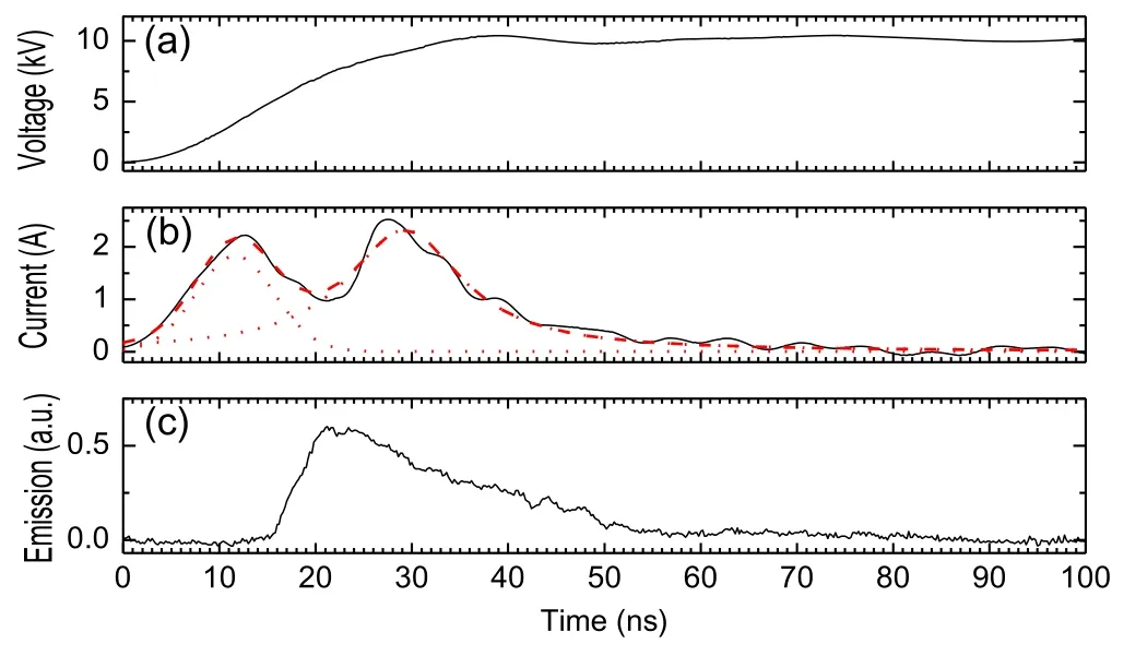
Figure 3.(a)Rising part of the driving high voltage pulse.(b)Induced total current(solid line),approximated by two Voigt functions(dot lines);the sum of the Voigt functions is also shown(dash line).(c)Induced optical emission.Operating conditions:10 kV;2 kHz;pulse width 2 μs.
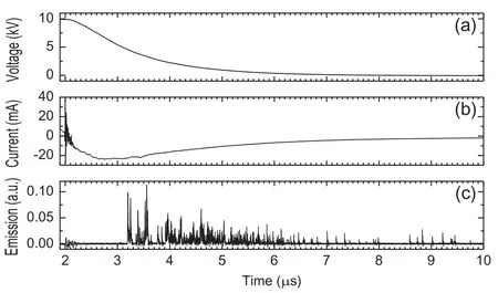
Figure 4.(a)Falling part of the driving high voltage pulse.(b)Induced total current.(c)Induced optical emission.Operating conditions:10 kV;2 kHz;pulse width 2 μs.
Figure 4 presents the corresponding waveforms recorded during the falling part of the driving voltage,under identical to figure 3 experimental conditions.In this case,the‘push mode’of the power supply(section 2)imposes a long fall time(roughly 2.5 μs;90%-10%).This relatively low slew rate leads to a weaker (about 100 times) and broader (more than 100 times)current waveform(figure 4(b))comparing to that of figure 3(b).On the other hand,figure 4(c) leads to a striking observation.Erratic emission impulses are recorded for a prolonged time,initiated at about 1 μs since the voltage decay has started and about 0.5 μs since the negative current has peaked.Contrary to figure 3,the current polarity indicates a negative net-charge drift away from the driven electrode,while the waveform approaches zero in an exponential way.In addition,the emission is long(about 10 μs in figure 4(c)) and the envelope of the erratic impulses reminds an exponential decay.Thus,it is speculated that these signals mirror charge displacement due to depolarization mechanisms(see discussion below).
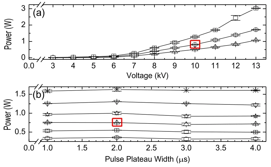
Figure 5.Electric mean power consumed by the plasma reactor,as a function of(a)the driving voltage pulse amplitude for various frequencies(Δ:1 kHz;○:2 kHz;□:4 kHz;2 μs everywhere)and(b)the driving voltage plateau width for various amplitudes(○:8 kV;□9 kV;Δ:10 kV;☆:11 kV;▽:12 kV;?:13 kV;2 kHz everywhere).Be aware of the break on the horizontal axis,before the 1 μs.The two framed points are commented in conjunction with figure 6 in the text.
In figure 5 the mean power of the reactor is given,parametrically.Higher voltage amplitude(figures 5(a)and(b))or frequency(figure 5(a))leads to increased power consumption;up to 3 W under the present operational windows.Figure 5(b)demonstrates that the width of the driving voltage pulse does not practically affect the consumed power,ceteris paribus.This is quite anticipated for the following reason.Any DBD setup has an equivalent electrical circuit where the impedance is dominated by a capacitanceCdieldue to the dielectric barrier.The induced current has thus a chief component equal toCdiel×,wherev(t)stands for the driving voltage.In the case of pulse train voltages,non-zero current values are obtained during the rising/falling edges of the pulses only,since during the pulse plateauv(t)=const.and thus the termequals zero.In turns,the instantaneous powerv(t)×i(t)should be null over the pulse plateau and the mean power is determined by the productv(t)×i(t)over the pulse transient slopes.In practice,the equivalent circuits of DBD setups are more complicated,including resistive and inductive components,and the waveforms delivered from commercial power supplies are far from ideal pulse trains.As far as the capacitive component is prevalent,the voltage pulse is free of important oscillations and the rise/fall time is independent of the duty cycle,the pulse width should not affect the mean power,like in our case.Similar results of almost constant mean energy as a function of the duty cycle have also been reported for other SDBD setups[63].In cases where the rise/fall time was duty-cycle dependent,the mean energy showed variations[87].However,the power consumption by DBDs cannot be fully interpreted based on circuitry terms only,since thermal effects,discharge dynamics,and plasma kinetics are distinctive for each setup.
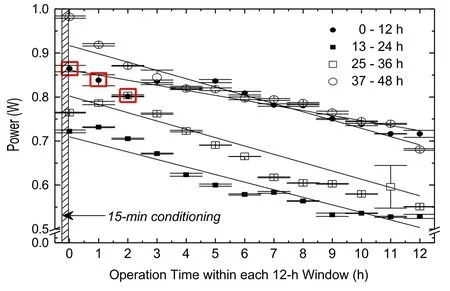
Figure 6.Electric mean power consumed by a newly fabricated plasma reactor,as a function of the accumulated operation time.Be aware of the break on the vertical axis,before the 0.5 W.A 12 h time window of continuous operation is considered per day,over four successive days(4×12 h).Mean values and standards deviations are calculated from three instantaneous measurements at the beginning of each 1 h step.Operating conditions:10 kV;2 kHz;pulse width 2 μs.The three framed points are commented in conjunction with figure 5 in the text.The shaded area marks out the 15 min conditioning period(see text).
Figure 6 delivers data on the mean power consumed by the reactor as a function of the time of continuous operation over long periods,at almost constant temperature and relative humidity (23°C and 49%,respectively).Namely,a newly fabricated reactor is employed and operated for 12 h per day for four successive days (4 × 12 h).For consistency reasons it is mentioned that,in practice,a 15 min plasma run precedes each 12 h window to allow to the reactor to be stabilized (e.g.thermally).This 15 min conditioning period is denoted by the line-pattern rectangular in figure 6.Otherwise,the power is measured at the early beginning of each 1 h step thrice,leading thus to the mean values and standard deviations given in figure 6.The data suggest that:(i)the power remains almost constant for measurements taken sequentially(see error bars);(ii)the power decreases within each 12 h window progressively;(iii) within each 12 h window there is a fluctuation pattern of the detrended power values(the trend is a declining straight line obtained by linear regression analysis);and (iv) between different 12 h windows there is not clear trend of the data (e.g.the power decreases from the 0-12 h to the 13-24 h window,but it recovers at 25-36 h and 37-48 h windows).
On the other hand,the measurements of figure 5 were carried out with a newly fabricated reactor within two successive days(one full set of data per day)and lasted about 45 min per set.Each set was preceded by a 15 min conditioning period as mentioned for figure 6 too.Hence,the operation time in figure 5 was about 1 h per day/set and the accumulated time was not more than 2 h (2 × 1 h).Consequently,one should expect the framed data of figures 5 and 6 to correspond to equal values.However,noticeable deviations do exist.It is speculated that any such inconsistency is attributed to the degradation of the electrodes which depends on the operation history.
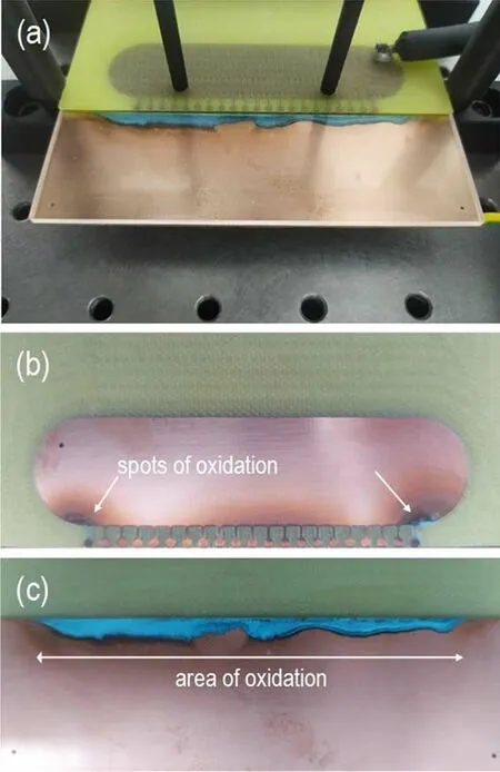
Figure 7.(a)Assembled reactor.(b)Disassembled anode electrode.(c)Disassembled cathode electrode.The photos refer to a newly fabricated reactor subjected to the four 12 h windows of figure 6.Operating conditions:10 kV;2 kHz;pulse width 2 μs.
Material degradation in SDBD reactors has extensively been reported in the literature,both for the electrodes and the dielectric barrier[70-73].In our case,the quartz plate remains unimpaired,whereas the cooper electrodes (and notably the cathode) are oxidized over time.Figure 7 sheds light on this effect and supports the speculation that power variations are principally related to repeated circles of ‘surface oxidationsurface cleaning’ due to plasma species bombardment.The control of these surface processes is beyond the scope of this work and has not been considered further on,as far as the experimental conditions and protocols are attested carefully.
A better insight to the discharge features is gained by the spectral results of figure 8.Although a much wider wavelength range has been investigated (see section 2 for grating specifications),only N2(SPS) andare detectable(figure 8(a)).Additionally,the rotational distribution of the N2(SPS) species (v′=0-v″=0;337.13 nm) is presented(resolution 2 pm),being determined both experimentally and numerically (figures 8(b) and (c)).The numerical fitting suggests a gas temperature around(307±40)K,i.e.quite low.
The results obtained are depicted in figure 9(a) where calculatedvalues at different vibrational sequences are plotted againstG(v′)values.By performing a linear regression of the data,an average vibrational temperature of(3080±70)K is found.To verify this value,the experimental vibrational spectra (figure 8(a)) are compared with simulated ones generated using the massiveOES software [89].An example is shown in figure 9(b) referring to the vibrational sequence Δv=-2 ((5) in figure 8(a)).In this case,the simulated spectrum approximates well the experimental one when considering aTvvalue of (3100 ± 100) K;figure 9(c)gives the residuals of this fitting.This temperature value is in good agreement with the value obtained from the Boltzmann plot in figure 9(a).Therefore,the rotational temperature,which in this case is characteristic of a cold atmospheric pressure plasma,is one order of magnitude lower thanTv.In other words,the present discharge is out of thermal equilibrium.
Recapping,the present setup generates surface discharges out of thermal equilibrium,correlated to low gas temperature,fast ionization/emission during the positive slope of the voltage,and slower ionization/emission during the negative slope of the voltage.
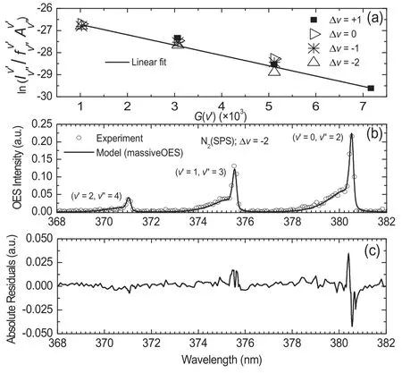
Figure 9.(a)Boltzmann plot using the vibrational sequences Δv=+1,0,-1,and-2 of N2(SPS)to determine the average N2(C)vibrational temperature from the slope of a linear regression line.(b)Experimental(open circles)and simulated(line)emission spectra of N2(SPS)corresponding to the vibrational sequence Δv=-2.(c)Absolute residuals of the fitting shown in the frame(b).
More concretely,as the voltage rises,cathode-directed streamers propagate.The ICCD images of figure 10 validate this scenario,showing the downstream propagation of the front of ionization waves emerging from the driven electrode array.In this figure,ΔtGDvaries(0-110 ns)so that the moving window ΔtGW(10 ns)sweeps progressively the high voltage pulse.For eachΔtGD,ICCD snapshots are accumulated from sequential voltage periods over a 0.5 s exposure time.The dark image of the first 10 ns(figure 10(a))and the ICCD intensity thereafter are in fair agreement with the PMT signal in figure 3(c).
Based on images like those of figure 10,the propagation speed of the front of the ionization wave is evaluated at the maximum amplitude of 12 kV.Due to the filamentary and erratic contour of the propagating front,the determination of the propagation length from the front contour becomes subjective.Thus,a simple image processing algorithm is here applied to the 1024×1024 grayscale images of the ICCD camera.The entries of each row of the matrix of each image are added up sidewise and thus an 1D vertical profile of the emission intensity is achieved.Then,any background offset is subtracted,and the end of the propagation length is considered to be coincident with the first(from up to down)row that gives an emission intensity ≤10% of the maximum value of the corresponding vertical profile.Figure 11 provides an indicative example.
Figure 12 gives the resultant instantaneous values of the propagation speed in comparison with the rising part of the voltage pulse.In a rough manner,three different phases may be considered,i.e.a launching one when the speed increases abruptly,a propagation one when the speed is quite constant,and an extinguishing one when the speed decreases gradually.However,the resolution of 10 ns is comparable to the rising time of the high voltage pulse (25 ns;figure 3) and thus not sufficient to fully capture the discharge dynamics.
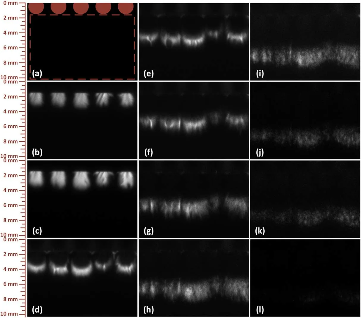
Figure 10.Top view ICCD images of the discharge.The red circles and dashed line in the frame(a)define the cropped part of the driven and the grounded electrode,respectively.Gate width ΔtGW=10 ns.Gate delay with respect to the beginning of the rising part of the high voltage pulse,ΔtGD (ns)/ICCD gain(a.u.):(a)0/230;(b)10/120;(c)20/70;(d)30/80;(e)40/100;(f)50/130;(g)60/160;(h)70/170;(i)80/170;(j)90/200;(k)100/200;(l)110/230.Operating conditions:10 kV;2 kHz;pulse width 2 μs.
Conversely,during the remaining part of the pulse plateau(120 ns to 2 μs)the ICCD camera does not detect any emission.Then,as the voltage pulse starts to decay slowly(figure 4(a)),weak emission within the vicinity of the driven electrode is detectable.Notably,ΔtGDmust be set at 2.9 μs in order to be able to detect the first emission,as figure 13(b)demonstrates.This observation is in fair agreement with the lag of the emission impulses in figure 4(c).Strictly speaking,in figure 4(c),the PMT signal becomes noticeable at about 3.2 μs,i.e.300 ns later than the ICCD indicates.This disparity is artificial for the following reason.
Referring to figure 1,ICCD collects light from the entire top-view of the discharge,whereas the PMT assembly from a side-on acceptance cone.According to figure 13(b),the discharge ignites from preferable points (usually from the middle of the driven electrode)and the emission is yet neither intense nor diffused.Thus,if the focusing probe is not aligned to this point of preference,the PMT signal will be negligible.At later moments,the emission becomes more intense and diffused,while eventually the discharge spreads over the entire driven electrode (figures 13(b)-(i)).Thus,photons may not enter the acceptance cone of the focusing probe from the beginning,depending on the focusing probe precise position.Experiments realized by mounting the focusing probe on a micro-translation stage,led to this conclusion.On the contrary,this is not an issue in figures 3 and 10 since the discharge ignites at once along the entire driven electrode (comparing figures 10(b)and 13(b)).Finally,it is noticed that at the time point around 2.9 μs the current peaks,negatively(figure 4(b)).
Furthermore,contrary to the case of figure 10 whereΔtGWis constant at 10 ns andΔtGDadjustable,in figure 13ΔtGDis constant at 2.9 μs andΔtGWadjustable.This has been done because during the decay of the voltage pulse,there is not propagation of any ionization front,as various tests have confirmed.Although the emission pattern expands downstream progressively,in a tassel-like form,it remains attached on the driven electrode.Thus,instead of shifting a fixed gate window by increasing the gate delay,a widening gate window is applied with respect to the fixed delay of 2.9 μs.This process gives practically the stitched snapshots of the emission up to the time point determined by the gate width.For eachΔtGW,ICCD snapshots are accumulated from sequential voltage periods over a 0.5 s exposure time.
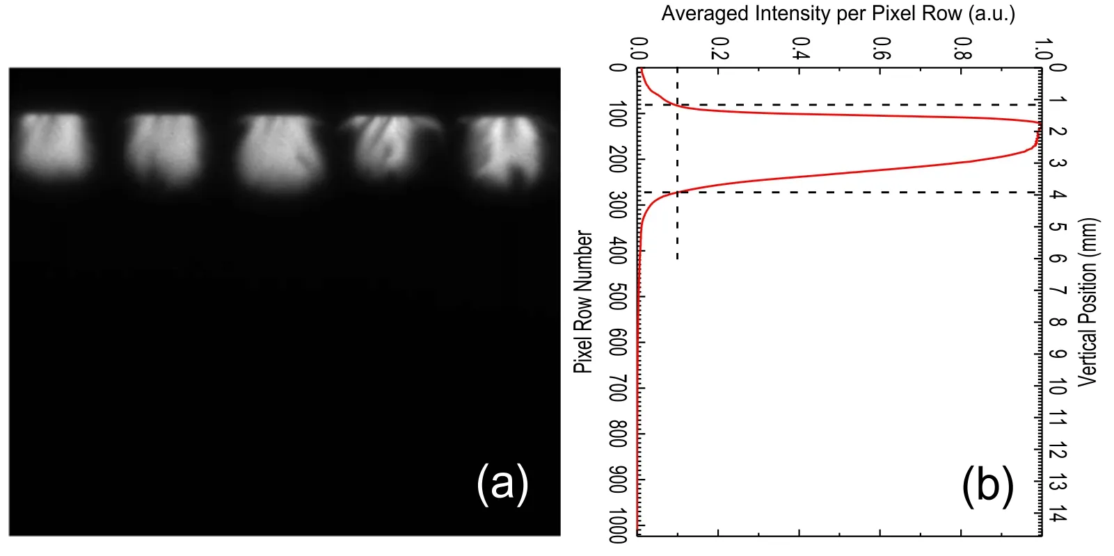
Figure 11.Image processing to define the propagation length of the ionization wave(see text for details).(a)Representative ICCD full image(1024×1024 pixels)as captured.(b)Plot of the optical emission intensity averaged over the 1024 pixel-columns for each individual pixel-row.The vertical dashed line indicates the 10%intensity level and the horizontal dashed line the considered propagation length(3.9-1.1=2.8 mm here).
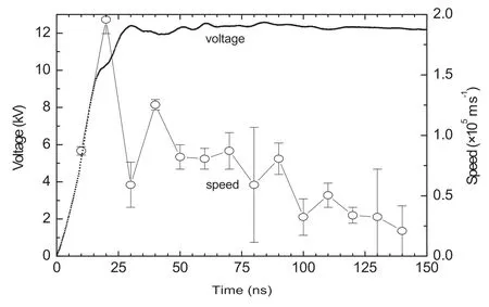
Figure 12.Instantaneous propagation speed of the discharge front with respect to the rising part of the high voltage pulse.Mean values and standard deviations are derived from 2 sets of images,like those of figure 10.Operating conditions:12 kV;2 kHz;pulse width 2 μs.
Figure 14 suggests the underlying mechanism involved in the results of figures 10 and 13,in a pictorial and quite simplified way(e.g.negative ions have been ignored).Symbols‘+’,‘-’,‘↗’,and ‘’ represent positive ions,electrons,dipolar moments,and photons,respectively.Before the external field application (figure 14(a)) there is a low-density background space charge,i.e.electrons and ions (not shown here),in the air gap and there exists no polarization in the dielectric barrier(dipole moments are randomly oriented in the bulk).The application of the electric field(figure 14(b))orients the dipoles to the corresponding direction;it is reminded that the dipole moment vector directs from the negative to the positive charge.Hence,the dielectric-barrier surface is charged with positive ions [82],balanced by electrons in surrounding positions accordingly.When the local net electric field(i.e.the resultant from the Laplacian field and the space charge field)attains an adequate value to cause gas breakdown(figure 14(c)),an ionization wave is propagating along the dielectric-barrier surface [50].This wave corresponds to a cathode-directed streamer.During this phase,positive surface charge is built up on the barrier due to the polarization of the latter and the external applied field is compensated.The launching,propagation,and extinguishing phases of this ionization wave were demonstrated above when figures 10 and 12 were commented.
Afterwards(figure 14(d)),the polarization of the dielectric is maximum and there is a depletion of electrons close to the surface of the dielectric barrier.This state is conservated as long as the voltage level remains constant(pulse plateau).As the external applied field decays(figure 14(e)),the polarization of the dielectric barrier is loosened.As a result,the number of bound positive ions and electrons diminishes,progressively.At the time that the field of the space charge outweighs the externally applied one (figure 14(f)),a second discharge is evolved.Now,the driven electrode acts as cathode[50].This discharge progression is demonstrated in figure 13.Finally(figure 14(g)),the field due to the positive surface charge becomes negligible and the electric dipoles inside the barrier tend to be randomly oriented.The dielectric barrier and the air gap approach now their initial state (figure 14(a)).The entire process implied by figure 14 is therefore repeated over the following high voltage pulses.However,a weak residual positive charge remains on the surface binding some electrons in steady state conditions[50,53,55,82].
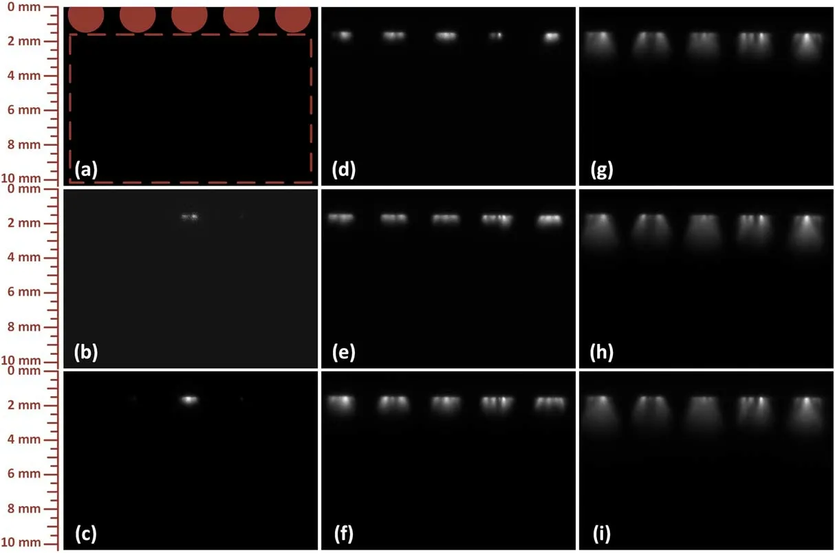
Figure 13.Top view ICCD images of the discharge.The red circles and dashed line in the frame(a)define the cropped part of the driven and the grounded electrode,respectively.(a)Dark images(gain 230)between 120 ns and 2.9 μs with respect to the beginning of the rising part of the high voltage pulse,independently of the gate width.Thus,the gate shift(delay) ΔtGDis fixed at 2.9 μs.Then,the gate width ΔtGW(ns)increases progressively/ICCD gain(a.u.):(b)50/170;(c)100/170;(d)200/100;(e)500/90;(f)1000/90;(g)2000/70;(h)4000/70;(i)6000/50.Operating conditions:10 kV;2 kHz;pulse width 2 μs.
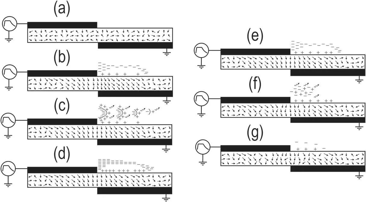
Figure 14.Conceptual and simplified mechanisms suggested with respect to figures 10 and 13.(+),(-),(),and(↗)represent positive ions,electrons,photons,and dipolar moments,respectively.(a)t=0- ns.(b)and(c)t=0+-120 ns;dielectric barrier polarization,background space charge separation,ionization wave front propagation,and surface charge built up.(d)t=120-2000 ns;external field compensation.(e)and(f)t≈2.0-12.9 μs;decay of the external field,cathode sheath formation,surface charge depletion,and dielectric barrier polarization decay.(g)12.9 μs<t<500 μs;quasi-depolarization and residual charge conservation.
Following the above interpretation,the dielectric properties of the barrier may play a determinant role in the discharge features.Dielectric permittivity is related to the dipole relaxation time and the surface charge density.This will have an impact on the local electric field evolution,as discussed above.Experiments with single-shot pulses [4]have shown that the length of the discharge depends on the relative permittivity.The larger the permittivity is the shorter the discharge length becomes.Other experiments with repetitive pulses [55] suggested that the use of a dielectric material onto which the surface charge decays faster,leads to well pronounced primary and secondary surface ionization waves having higher velocity on the voltage rising part.In addition,both the peak current and the peak electric field are found to be higher,with lower spatial attenuation along the surface ionization wave propagation path.Besides,the discharge length has been found to decrease for increased permittivity,according to experimental and modeling results[62].Further models [82] indicate that in a unipolar mode,residual surface charges suppress the development of discharges and energy deposition.Hence,the influence of the dielectric material to the SDBD properties appears unambiguous and in the present work quartz is employed due to its durability comparing to other materials tested in our previous work[70].
4.Discussion
The results unfolded and discussed above were achieved by the combination of different diagnostic techniques,applied all together to a single SDBD setup under identical conditions.Hence,complementary view on fundamental properties of a SDBD was obtained,in terms of voltage,current,and optical emission waveforms,power consumption,material endurance,reactive species,rotational and vibrational temperatures,and discharge dynamics.This last section emphasizes some key points of the present work.
Firstly,the common practice of the use of foil adhesive tapes and stack of dielectric layers for handmade SDBD setups,leads unavoidably to limited design reproducibility among different batches of the setups,dimension tolerance,uncontrollable air cavity formation,electrode irregularities,partial discharges,short lifespan,etc.These issues may highly affect the results when fundamental studies are carried out,while make the round-robin tests worthless.The SDBD setup implemented in this work is not handmade,in the sense that both the dielectric barrier and the electrode patterns are standardized.However,it is vulnerable due to the copper oxidation and periodic maintenance is necessary (e.g.soft abrasion).On the contrary,quartz showed to be an excellent dielectric for SDBD fundamental studies,extending the lifetime of the setup substantially.It is admitted that a few works introducing PCB-based SDBD setups do exist[90-94],but the dielectric barrier is formed by the PCB dielectric itself which is a rather degradable material(usually consists of glass epoxy or cotton paper impregnated with phenolic resin).
Then,the present SDBD setup is driven by high voltage pulses of asymmetric edges,i.e.short rising and long falling times.This implies a sort of novel modulation of the discharge,leading to diverse ionization/excitation effects along the driving pulse.SDBD features can potentially be tailored by adjusting those times.
Finally,there is a long debate on the current waveform pattern in the cases of SDBDs.More concretely,the double peak recorded in this work (figure 3) has been observed by other authors,but its interpretation may differ between different reports.Jiang et al [95] developed a plasma fluid model of ns-pulsed SDBD and the existence of the two current spikes was verified.They were attributed to the two phases of the discharge: propagation of the ionization wave and reignition in the gap between the latter and the dielectric surface.Komuro et al [96] demonstrated the two peaks experimentally,without further comments on their origin.Kettlitz et al[66]claimed that the steep voltage rise(and drop)caused a high displacement current of up to about 150 mA overlapping the discharge current.The discharge current during the rising slope could be recognized as a small peak at about 40 ns when the discharge ignited at approximately 7 kV.In this case,the maximum discharge current was about 80 mA.During the falling slope,the discharge current was much lower and hardly detectable.Unfer and Boeuf[50]found numerically that the first current pulse started during the voltage rise,passed through a first maximum at about 5 ns,slightly decayed(due to the charging of the surface),and increased again (because of the continuous increase in the applied voltage) and reached a second maximum,on the order of 103A m-1,at the end of the voltage rise.The numerical model of Soloviev and Krivtsov[78] showed that the rising time of the narrow peak on the electric current at the leading edge of a negative polarity voltage pulse contained two steps of different slopes.The first step (about 1 ns duration) was ascribed to fast electron-ion breeding and cathode layer formation;the second step(appeared up to 2.5 ns) referred to be a further modification of the cathode region at higher absolute voltage.In the present work,the correlation between the current signals,the PMT signals,and the ICCD images points clearly to the quartz charging and the DBD ignition as the origin of the first and second current peak,respectively.
5.Conclusions
Surface ionization waves generated by pulsed dielectric-barrier discharges were studied experimentally.The consumed electric power was found to increase almost quadratically with the driving voltage amplitude and monotonously with the corresponding frequency,whereas it remained almost constant with the pulse width.On the other hand,prolonged continuous operation was related with decreasing power consumption,implying electrode surface degradation.Conversely,quartz demonstrated a noticeable stability as a dielectric barrier for surface discharge studies.Molecular nitrogen excited neutrals and ions were the main emissive species of the discharge,while the overall gas temperature was sustained quite low.The discharge was identified to be the result of cathode-directed ionization waves,propagating at velocities close to 105m s-1during the fast-rising part of the driving voltage,and being interrupted due to the surface charge built up on the dielectric barrier surface.Finally,the slow-falling part of the driving voltage was found to be associated with the formation of cathodic sheath on the driven electrode.
Acknowledgments
The authors express their gratitude to Mr.Konstantinos Petrou(University of Patras,Department of Electrical and Computer Engineering) for his valuable technical support (PCB fabrication).
Data availability statement
The data that support the findings of this study are available from the corresponding author upon reasonable request.
ORCID iDs
 Plasma Science and Technology2023年11期
- Plasma Science and Technology的其它文章
- High-order field theory and a weak Euler-Lagrange-Barut equation for classical relativistic particle-field systems
- Design of new resonant magnetic perturbation coils on the J-TEXT tokamak
- Non-invasive optical characterization and estimation of Zn porosity in gas tungsten arc welding of Fe-Al joints using CR model and OES measurements
- A study of grid failure mode drivers and methods for accelerated life testing of a 30cm diameter ion thruster
- Research on degradation mechanism of trichlorobenzene and Hg0 by nonthermal plasma catalysis
- Development of an atmospheric fluorocarbon plasma jet generated by pulse modulated microwave discharge