
Valley polarization in transition metal dichalcogenide layered semiconductors: Generation,relaxation,manipulation and transport
2023-11-02 08:37:22HuiMa馬惠YaojieZhu朱耀杰YulunLiu劉宇倫RuixueBai白瑞雪XilinZhang張喜林YanboRen任琰博andChongyunJiang蔣崇云
Chinese Physics B 2023年10期
關(guān)鍵詞:瑞雪
Hui Ma(馬惠), Yaojie Zhu(朱耀杰), Yulun Liu(劉宇倫), Ruixue Bai(白瑞雪),Xilin Zhang(張喜林), Yanbo Ren(任琰博), and Chongyun Jiang(蔣崇云),?
1School of Physical Science and Technology,Tiangong University,Tianjin 300387,China
2College of Electronic Information and Optical Engineering,Nankai University,Tianjin 300350,China
Keywords: valley polarization,nonmagnetic transition metal dichalcogenide layered semiconductors,exciton
1.Introduction
Encoding information based on spin or valley degree of freedom is promising due to their low-power dissipation and fast processing speed.When the latter is used, it is classified as valleytronics.[1-3]The valley represents the local extremum point in the band structure in momentum space.In nonmagnetic transition metal dichalcogenide(TMD)semiconductors,there are two inequivalent valleys at+Kand-Kpoints,which can be labeled by a binary pseudospin.The application of valleytronic devices strongly depends on the carrier population distribution polarized in+Kand-Kvalleys,which is referred to as valley polarization.[4-6]It is preferable to have a high degree of valley polarization and a long valley-polarized lifetime.
Monolayer TMD semiconductors exhibit direct bandgap,large exciton binding energy, and strong spin-orbit interaction, which makes them an attractive platform for exploring valley physics and applications in valleytronics.[7-9]The broken inversion symmetry in monolayer TMD gives rise to spinvalley locking,[10]which enables exclusive valley-dependent optical selection rules in +Kand-Kvalleys.The coupling between optical signals and valley excitons facilitates information initialization and read-out.In addition,spin-valley locking allows to manipulate valley information by managing spin,such as by generating valley polarization via the injection of spin-polarized carriers.[11-14]Based on the TMD monolayer,the heterostructure, assembled with a few layers of different TMD materials via a weak interlayer van der Waals force,hosts long-lived interlayer excitons due to spatially separated electrons and holes in different layers, making it a promising system for future valleytronic devices.[15]Moreover, adjusting the twist angle between layers could result in further valley physics manipulation.[16,17]Therefore,valley polarization based on TMD layered semiconductors has received much attention recently.
In this review, we focus on valley polarization in the nonmagnetic TMD monolayer and its hybrid hetero/homobilayers.We start by introducing the valley physics and valley information carrier of excitons in TMD semiconductors.We then comment on approaches to generate valley polarization,including optical pumping with circularly polarized excitation and electrical spin injection via ferromagnetic semiconductors or metals.In view of the dynamic stability of valley information,depolarization and relaxation of valley polarization are discussed after that.In light of the imperfect initialization of valley polarization, strategies to manipulate and improve valley polarization are reviewed.These involve employing gate voltage to induce electrostatic doping or tune outof-plane dipole moments, applying a magnetic field or magnetic proximity effect to produce band offset and valley Zeeman shift,and utilizing moir′e pattern with spatially modulated selection rules for optical transitions.Whereafter, the transport, referring to the diffusion and separation of valley polarization,is discussed.After that,we briefly discuss valleytronic devices, including valley light-emitting diodes (LEDs) and valleytronic transistors.Finally, we provide a summary with an outlook and challenge for future research on valley polarization and its practical applications in TMD-based semiconductors.
2.Valley physics and valley excitons
In the hexagonal 2D layered materials, such as TMDs,there are two inequivalent valleys with energy degenerate band edges(±K)at the corners of Brillouin zone(Fig.1(a)).These valleys operate as a binary pseudospin and offer another degree of freedom in addition to charge and spin.In monolayer TMD,the broken inversion symmetry gives rise to spin-orbit coupling, which induces spin splitting in each valley.The time-reversal symmetry dictates spin down(up)in the+Kvalley to be degenerate with spin up(down)in the-Kvalley,resulting in spin-valley coupling (Fig.1(b)).[10]This coupling allows the manipulation of valley properties by controlling the spin.
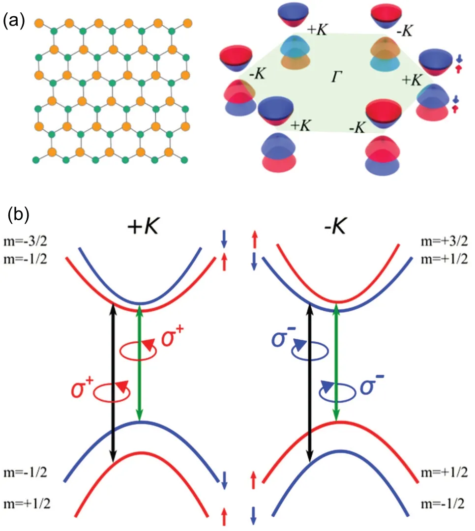
Fig.1.The 2D hexagonal lattice and valley physics.(a) 2D hexagonal lattice of a monolayer TMD consisting of chalcogen atoms(green)and transition metal atoms (orange), and the first Brillouin zone with two inequivalent K points in disulfide of tungsten.(b)Spin-valley coupling and valley-dependent optical selection rules for A excitons(green double sided arrows)and B excitons(black double sided arrows)at two valleys. m is the azimuthal quantum number of the total orbital momentum. σ+ (σ-)circularly polarized light couples with+K(-K)valleys because only transitions with Δm=+1(-1)are allowed.
The broken inversion symmetry also results in the valleycontrasting Berry curvature and orbital magnetic moment,which offer an effective way for controlling the valley degree of freedom.[18-20]The Berry curvature is analogous to a magnetic field in that it causes an anomalous velocity transverse to the applied electric field,i.e.,the Hall effect,including the spin Hall effect and the anomalous Hall effect in spin-orbit coupled systems.The orbital magnetic moment is caused by the electron wavepacket’s self-rotating motion.It permits the valley pseudospin to be coupled with a magnetic field,allowing the valley polarization to be detected as a magnetic signal.The valley-dependent phenomena of Berry curvature and orbital magnetic moment will be discussed in the subsequent sections.
In TMD semiconductors, excitons, which are composed of electrons and holes via the Coulomb interaction, are the dominant quasiparticles to convey valley information owing to the localization of the constituent electrons and holes in the+Kand-Kvalleys.Excitons behave as stable carriers of valley information because their binding energy,which can reach hundreds of meV,is higher than the thermal activation energy at ambient temperature.[8]There exist several types of excitons according to their components,such as the neutral bright(dark) exciton consisting of an electron and a hole with spin conservation(flip),the charge exciton,i.e.,trion,with the neutral exciton capturing an extra electron or hole, and the biexction composed of two electrons and two holes.[9]Different excitons can be distinguished by photoluminescence spectra due to their distinct binding energies.Besides,different excitons possess different physical origins and distinct sensitivities to electrical gating,optical density,and magnetic field,providing a degree of freedom to manipulate the excitonic response in different applications.[21-24]
3.Valley polarization
Valley polarization refers to the imbalanced carrier population between+Kand-Kvalleys,[25-27]which distinguishes binary valley information and supplies a practical platform for information processing.Valley polarization with a high initial degree, a long-lasting lifetime, and long-range transport are necessary for valleytronic devices.In this part,we present recent progress on the generation,relaxation,manipulation,and transport of valley polarization in nonmagnetic TMD layered materials.
3.1.Generation of valley polarization
There are mainly two approaches to generate valley polarization,one of which is the optical pumping with circularly polarized light.In theory, orbital magnetic moments enable the valley pseudospin link to a magnetic field, which creates the valley-dependent optical selection rules,[10,28]i.e., the interband transition in the+K(-K)valley couples exclusively to theσ+(σ-)circularly polarized light(Fig.1(b)).The valley polarization is usually determined in experiments by the polarization-resolved photoluminescence (PL) spectroscopy,which can be defined by the circular polarization as
whereI(σ±)is the intensity of the left-and right-handed circular component.Mak and Zenget al.[25,26]reported the first experiment in monolayer MoS2almost at the same time.They discovered that the valley polarization switched when the excitation changed fromσ+toσ-circularly polarized light(Fig.2(a)).Besides, the valley polarization was observed to be sensitive to the excitation photon energy(Figs.2(b)-2(e)),reaching a maximum with on-resonance excitation.Hereafter,valley polarization in other TMD monolayers and their hybrid bilayers was investigated.Valley polarization in these systems ranges from 30% to nearly 100%.[25,26,29,30]The less-than-perfect degree of polarization is mainly attributed to intervalley scattering[29,31]and the electron-hole exchange interaction.[32,33]On-resonance excitation is one strategy to enhance the valley polarization, which could significantly decrease the phonon-mediated intervalley scattering or the electron-hole exchange interaction.Kioseoglouet al.[29]have demonstrated a threshold of twice the LA phonon energy,beyond which phonon-assisted intervalley scattering gives rise to depolarization.Almost complete depolarization occurred when the excitation is about 100 meV above the threshold energy.
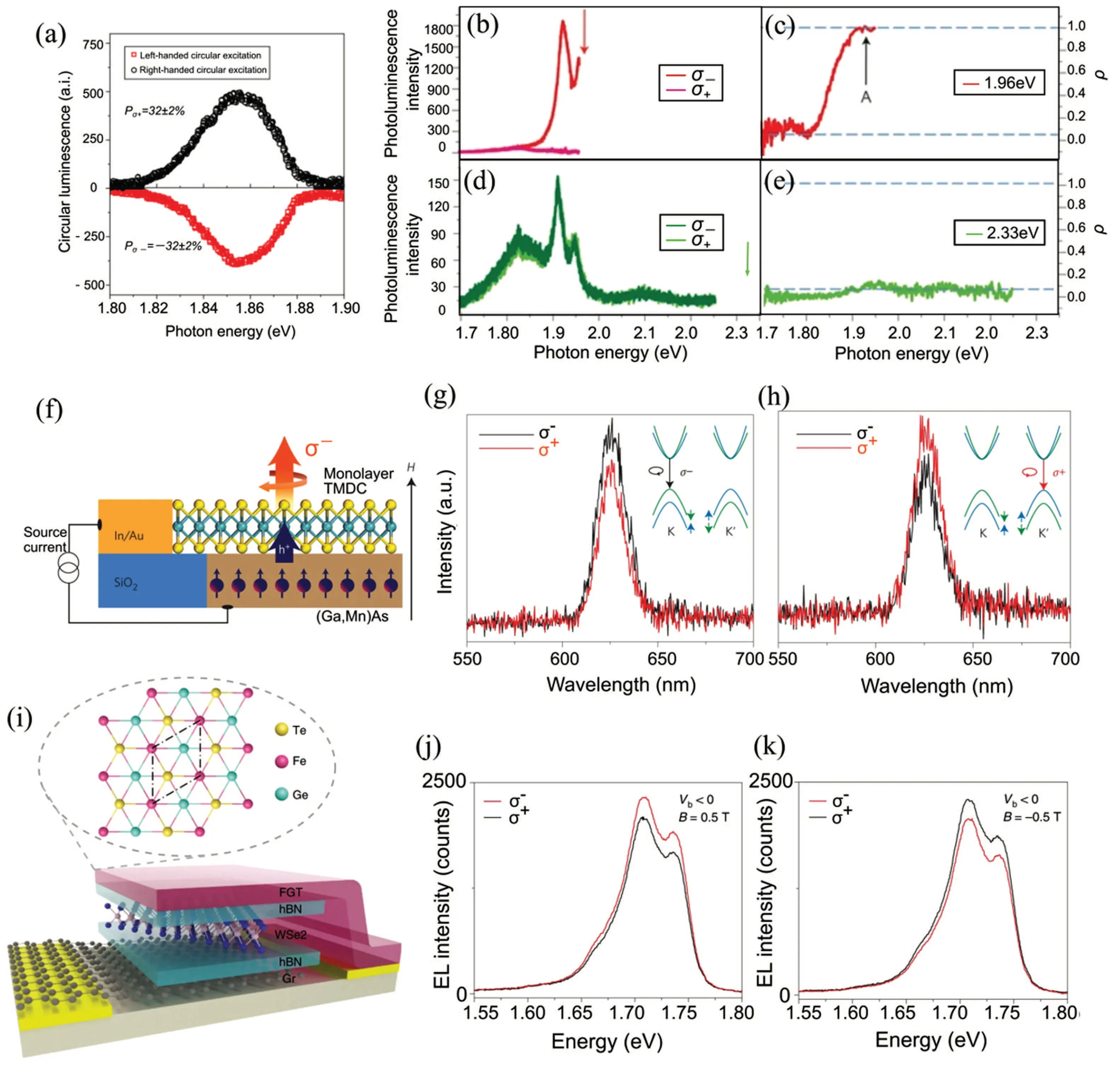
Fig.2.Optical (a)-(e) and electrical generation (f)-(k) of valley polarization.(a) Polarization-resolved PL spectra under left-handed (black symbols)and right-handed(red symbols)circular excitation in monolayer MoS2 at 1.96 eV and 10 K.[26](b)-(e)Helicity-dependent PL spectra and corresponding circular polarization ρ for σ-excitation at 1.96 eV(on-resonance,(b),(c))and 2.33 eV(off-resonance,(d),(e))in monolayer MoS2.[25] (f)Schematic for an electrical valley polarization device using monolayer TMDC/(Ga,Mn)As heterojunction.(g),(h)σ+ and σresolved EL spectra under an outward(g)and inward(h)magnetic field of 400 Oe perpendicular to the surface of device(f).Inset: diagram of the electrical excitation and emission processes.[13] (i)Schematic of vertically stacked FGT/hBN/WSe2/hBN/graphene heterostructures.(j),(k)Polarization resolved EL spectra for σ+ and σ- detection under a negative bias Vb,outward(j)and inward(k)magnetic field to the surface of device(i).[12] Figure reproduced with permission from(a)Ref.[26],Nature Publishing Group;(b)-(e)Ref.[25],Nature Publishing Group;(f)-(h)Ref.[13],Nature Publishing Group;and(i)-(k)Ref.[12],Nature Publishing Group.
In addition to the optical generation of the valley polarization, which may facilitate the development of optovalleytronic devices, another approach is the electrical generation through spin injection via a diluted ferromagnetic semiconductor.Pioneering work was performed in the n-WS2/p-(Ga,Mn)As heterojunction,[13]where the ferromagnetic semiconductor of (Ga, Mn)As supplies an out-of-plane magnetic easy axis as a spin aligner and allowed spin-polarized hole injection at forward bias (Fig.2(f)).The degree of valley polarization of this heterojunction was confirmed from the polarization-resolved electroluminescence (EL) spectroscopy(Figs.2(g)and 2(h)).The EL helicity is found to approach a maximum of 16.2%.When the applied magnetic field is inverted,an opposite EL helicity of-14.8%is obtained.This is because the +Kvalley is preferentially injected with spin-up holes from spin-polarized(Ga,Mn)As due to spin-valley locking(inset of Figs.2(g)and 2(h)),which leads toσ-emission as a result of optical selection rules.The reversed magnetic field enables the injection of spin-down holes into the inverted valley-K,resulting inσ+emission.This work demonstrates the electric generation of the valley polarization with spin injection as a new perspective of electronic devices for future information processing.
However, the use of a magnetic substrate for spin injection limits further development of integrated valleytronic devices.Hereafter, spin-polarized charge carriers injected by local permalloy electrodes[11]and van der Waals (vdW) ferromagnetic metal were demonstrated.[12,14]As another route of electrical generation of valley polarization, utilizing vdW ferromagnetic metal as a spin injector has the potential to be integrated with TMD to form vdW heterostructures without lattice-mismatching constraints.One promising candidate for vdW ferromagnetic metal is Fe3GeTe2(FGT),which has a Curie temperature higher than 130 K and possesses a single magnetic domain together with large coercivity and strong perpendicular magnetic anisotropy.Liet al.[12]fabricated a vertically stacked heterostructure composed of FGT/hBN/WSe2/hBN/graphene with FGT as the spin injector into monolayer WSe2under a bias voltage(Fig.2(i)).EL helicity was observed at a negative voltage and external magnetic field (Figs.2(j) and 2(k)), which flips sign when the external magnetic field changes to the opposite direction and is still preserved even though the magnetic field is removed.They further confirmed the role of FGT by elevating the temperature to higher than its Curie temperature and replacing ferromagnetic FGT with nonmagnetic graphene, which results in the EL helicity vanishing.It is anticipated that valley polarization near room temperature may be realized when the FGT electrode is replaced with ferromagnetic metals working near room temperature,such as Fe5GeTe2(TC~270 K)and MnSex(TC~300 K).[34-36]
3.2.Relaxation of valley polarization
Exciton lifetime and valley-polarized lifetime are two important parameters for valleytronic devices, which reflect the dynamic stability of valley information.The valley lifetime can be shorter or longer than the exciton lifetime(recombination lifetime).Their relative magnitude could highly influence the degree of valley polarization.The valley polarization and the two lifetime parameters are related by[37]
whereP0is the initial degree of circular polarization,τis the recombination lifetime,τvis the valley lifetime.[38]If the valley lifetime is longer (shorter) than the recombination lifetime, high (low) valley polarization is expected.In monolayer TMD, the strong electron-hole exchange interaction is the dominant depolarization mechanism of excitons, resulting in exciton lifetime and valley lifetime in the order of picoseconds.[39-41]In contrast,trion lifetime is prolonged because the dominant mechanism of intervalley scattering demands spin flips of individual carriers, which are energetically and spin forbidden for trions.[42]Bound exciton, stemming from the localization of impurities, defects, or strains in monolayer (ML) TMDs, enables the valley lifetime to reach the microsecond level.[43]Besides,experiments in MLWSe2have shown that the dark excitons and dark trions,lying tens of meV below the bright exciton, depolarize on a time scale of hundreds of picoseconds and several nanoseconds,respectively.[44,45]
In TMD heterostructures, electrons and holes are separated in two monolayers, forming interlayer excitons, which possess longer exciton lifetime and valley lifetime due to greatly reduced electron-hole exchange interaction.Riveraet al.[15,46]have observed exciton lifetime of 1.8 ns at 20 K and valley lifetime of 40 ns at 30 K in WSe2/MoSe2heterostructures.Scuriet al.[47]have demonstrated long valley lifetimes exceeding 40 ns in twisted WSe2-WSe2bilayers.Huanget al.[48]have achieved valley lifetime of 1 ns at room temperature by transferring WSe2/MoS2heterostructures to a silicon suspended slab.Nanosecond or even microsecond scale of(valley)lifetime of interlayer exciton makes vdW heterostructures a promising platform to study valley exciton physics and explore novel valleytronics and spintronics devices.[49,50]
3.3.Manipulation of valley polarization
Valley polarization with a high polarization degree and a long lifetime is desirable for the development of valleytronic devices with energy-efficient information coding and processing.However,nonmagnetic TMD semiconductors have a limited range of intrinsic valley properties.Thus,several manipulation methods,including electrical gating,magnetic field and magnetic proximity effect, and moir′e pattern, have been explored.
3.3.1.Electrical gating
Electrical gate manipulation of valley properties is effective in natural bilayer TMD because the intrinsic inversion symmetry can be broken.It has been reported that in bilayer MoS2,the circularly polarized PL could be continuously tuned from-15% to 15% by gate voltage, whereas in monolayer MoS2with intrinsic broken inversion symmetry,the PL polarization is gate independent.[51]This phenomenon is attributed to the continuous variation of orbital magnetic moments between positive and negative values through symmetry manipulation.
Electrical gate can act as electrostatic doping to manipulate the valley polarization.As discussed above, the longrange e-h exchange interaction dominates the intervalley scattering process in ML TMD, which results in short valley lifetime.Electrostatic doping could induce screening effect,which suppresses the long-range e-h exchange interaction and thus improves the degree of valley polarization and valleypolarized lifetime.[30,52-54]Zhanget al.[55]have reported that the degree of valley polarization in ML-MoTe2could be increased to 38%for excitons and 33%for trions through electrical manipulation(Figs.3(a)and 3(b)).The valley-polarization lifetime could be extended by a factor of 1000 to nanoseconds by converting excitons to trions through gate control(Fig.3(c)).Shinokitaet al.[56]have demonstrated an enhancement of the valley polarization from about 20% to 40% via electrostatic doping,which is ascribed to the prolonged valley lifetime induced by the weakened e-h exchange interaction.Similar experimental results have also been reported in MLWS2and ML-MoS2.[6,57]

Fig.3.Gate voltage manipulation of the valley polarization.(a) Schematic of the electrically gated ML-MoTe2 device.(b) The gate-dependent circular polarization degree of excitons(black dots)and trions(red dots).The neutrally charged region(NCR)is shaded in yellow.(c)The gate-dependence of fitted intravalley decay time 1/(black dots) and intervalley decay times 1/ΓTir(blue dots) of trions.[55] (d) Cartoon depiction of MoSe2/WSe2 heterostructure and the interlayer exciton with a permanent out-of-plane dipole.(e)Time-resolved PL of interlayer exciton at different gate voltages.The blue curves display the decay of valley polarization.Lifetimes of 39 ns, 10 ns, and 5 ns for gate voltages of +60 V, 0 V, and -60 V are obtained from single exponential fits,respectively.[46](f)Schematic of a TMD homo/heterojunction devices with dual gates.[16](g),(h)Degree of circular polarization(DOCP)as a function of outof-plane electric field(g)and doping density(h)in twisted WSe2-WSe2 bilayers. X0 and XI denote intralayer excitons and interlayer excitons,respectively.[47](i)The circularly polarization(ΔIRL)as a function of the gate voltage VTG with σ+ polarized excitation.Insets show the excitation and emission polarization in different voltage ranges.[58] Figure reproduced with permission from(a)-(c)Ref.[55], Nature Publishing Group; (d), (e)Ref.[46], AAAS;(f)Ref.[16],Nature Publishing Group;(g),(h)Ref.[47],American Physical Society;(i)Ref.[58],Nature Publishing Group.
Electrical gate control also plays an important role in TMD homo/heterobilayer.In this system, interlayer excitons possess an out-of-plane dipole moment due to the electrons and holes being separately located in two monolayers(Fig.3(d)).Thus, apart from the carrier doping, gate voltage can also modulate the dipole moment and vary the electronhole wavefunction overlap.In MoSe2/WSe2heterostructures,it has been reported that the valley polarization of interlayer excitons decays with lifetimes of about 39 ns,10 ns,and 5 ns for gate voltages of+60 V,0 V,and-60 V,respectively,which can be seen in Fig.3(e).The valley polarization of interlayer exciton reaches a maximum of about 40% at +60 V.[46]The long-lasting valley polarization and maximum degree of valley polarization that emerged at positive gate voltage can be interpreted by a decrease in oscillation strength and intervalley scattering resulting from a reduction of electron-hole wavefunction overlap of the interlayer excitons.
To distinguish between the electrostatic doping and electric field effects on interlayer excitons, homo/heterojunction devices with dual gates have been designed and developed,as shown in Fig.3(f).Such devices are usually composed of the hetero/homobilayer encapsulated with bottom and top h-BN, outside of which bottom and topmost graphite serve as the electrodes to assist in light absorption and emission.Top gate and bottom gate can be assigned appropriate values according to the thickness of the bottom and top h-BN so as to independently control the out-of-plane electric field and electrostatic doping of the device.[59]
Scuriet al.[47]have investigated the electric field dependence of the degree of circular polarization (DOCP) of interlayer excitons in twisted WSe2/WSe2bilayers(Fig.3(g)).The linear stark effect is a typical signature of the interlayer excitons due to their out-of-plane dipole moment.An electronhole separation of 0.37 nm was extracted from the slope,which is smaller than the interlayer spacing,indicating at least one of the carrier wave functions is partially delocalized between the layers.This work suggested that interlayer excitons consist of electrons fromQpoint of the conduction band and holes formKpoint of the valence band.Therefore, electric field control of interlayer excitons could reveal the band extrema.The doping dependence of the DOCP of interlayer excitons is shown in Fig.3(h), which exhibits around 80%in the n-doped regime and almost zero in the p-doped regime.The strong asymmetry in the DOCP results from the interplay between valley depolarization and exciton decay dynamics.They also found the valley lifetime could be tuned by more than three orders of magnitude via electrostatic doping.
Ciarrocchiet al.[58]have realized a circular polarization switch in a MoSe2/WSe2heterostructure from almost unity to around-50%by dual-gating control in the electrostatic doping mode.The circular polarization(ΔIRL)as a function of the gate voltage is presented in Fig.3(i).When the gate voltage is between 0 V and 5 V, positive ΔIRLindicates the emission polarization preserved the input polarization,acting as the polarization transmitter(inset in Fig.3(i)).In contrast,when gate voltage is outside the range of 0-5 V,negative ΔIRLreveals the emission polarization switching the input polarization, working as a polarization inverter.This result could be explained by the alteration of the moir′e potential caused by the electrostatic doping,which changes the exciton localization from one minimum to another in the moir′e pattern with different local symmetry and light coupling rules.Details about the moir′e pattern will be presented below.
3.3.2.Magnetic field and magnetic proximity effect
Time-reversal symmetry permits the intrinsic energy degeneracy of two valleys in nonmagnetic monolayer and multilayer TMD structures.This degeneracy can be lifted by applying a magnetic field.In analogy to the spin Zeeman effect,the interaction between the magnetic field and the valley magnetic moment gives rise to the valley Zeeman effect.[41,60]Valley Zeeman shift induces large band offsets between two valleys(Fig.4(a)), which provides a powerful tool to manipulate the valley degree of freedom.
It has been reported that magnetic-field-modulated valley polarization of excitons or interlayer excitons linearly increases at a rate from 1%/T to 7.7%/T in nonmagnetic TMD monolayer and bilayer (Table 1).[61-66]This is because the magnetic-field-induced valley Zeeman effect pushes specific valleys in the energy spectrum up and down, expanding the differences in exciton populations between two valleys.Moreover,the band offset reduces the intervalley scattering and results in an increase in valley polarization.As a consequence,valley polarization approaching 100%is expected if the magnetic field is strong enough,which has been demonstrated in a MoS2/MoSe2/MoS2heterostructure(Fig.4(b)).[67]
Applying a magnetic field not only significantly increases the degree of valley polarization but also prolongs the valleypolarized lifetime.[49,65]Our research group extended the valley-polarized lifetime of interlayer excitons from 15 ns at 0 T(Fig.4(c))up to 1.7μs at-3 T(Fig.4(d))in MoSe2-WSe2heterostructures.We demonstrated that the microsecond scale of lifetime was contributed by the transfer process of dark to interlayer excitons(Fig.4(e)),where the intervalley scattering rate of dark excitons is substantially smaller than that of bright excitons due to the relatively smaller exchange interaction between dark excitons.
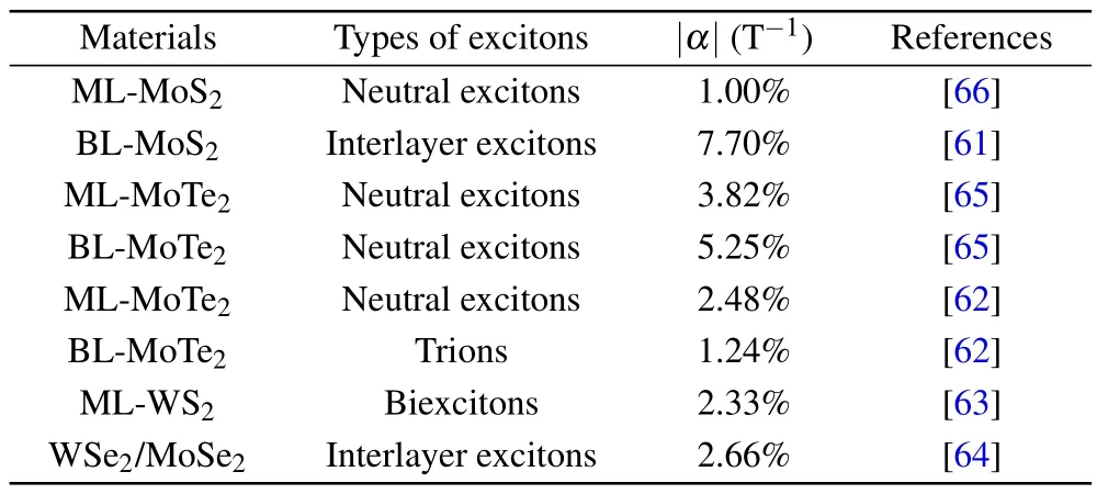
Table 1.Magnetic modulation factor of valley polarization.Magnetic modulation factor α=ρ/B,where ρ is the valley polarization,and B is the magnetic field.ML and BL are abbreviations for monolayer and bilayer,respectively.

Fig.4.Magnetic field manipulation of the valley polarization.(a)Energy level without(left side)and with(right side)out-of-plane magnetic field.Valley Zeeman shifts are shown by short dotted lines.(b) Magnetic field dependence of circular polarization in a MoS2/MoSe2/MoS2 heterostructure under σ- polarized excitation of 740 nm.[67] (c), (d) Dynamics of valley polarization.At BZ =0 the valley polarization is hardly seen after 50 ns and has a decay time of 15 ns (c).At BZ =-3 T, the valley polarization can be seen even at 200 ns, corresponding to a decay time of 1.745 μs (d).(e) The two conversion routes from the WSe2 dark exciton to the interlayer exciton.In the right-side and left-side routes, the spin flip happens before and after the interlayer charge transfer, respectively.The transition rate for the right-side route is exponentially dependent on the magnetic field,while it is a constant for the left-side route.[49] Figure reproduced with permission from(b)Ref.[67],American Chemical Society;(c)-(e)Ref.[49],Nature Publishing Group.
In addition to applying a magnetic field,the time-reversal symmetry of nonmagnetic TMD semiconductors can be broken by proximity to magnetic layered materials or substrates,giving rise to an interfacial magnetic exchange field in TMD semiconductors, which offers an effective method for valley control.By transferring the monolayer WS2onto the LaMnO3ferromagnetic substrate, Danget al.[68]observed a considerably improved valley polarization of up to 80%in monolayer WS2under nonresonant excitation at 4.2 K.The temperature dependence of the valley polarization indicates the excitonmagnon coupling between WS2and LaMnO3.They proposed that the nonradiative transfer of photoexcited energy to the LaMnO3or the formation of interlayer excitons decrease intervalley scattering and thus boost valley polarization.Castroet al.[69]recently claimed that the magnetic proximity effect from a ferromagnetic substrate could increase the valley polarization of interlayer excitons in MoS2/WS2heterostructures.They proved that the phonon-assisted intervalley scatterings between two split interlayer exciton states in two valleys promote the population imbalance of intervalley exciton,resulting in the enhancement of valley polarization.
The valley polarization of the TMD monolayer could be further modulated via the magnetic proximity effect by applying gate voltage or adjusting the optical excitation power.Liet al.[70]employed electrical gating to switch valley polarization in monolayer WSe2coupled with a magnetic insulator, CrI3.This switching is thought to occur as a result of the gate control of the interlayer spin-flip transition in 2D CrI3.Zhanget al.[71]enlarged the valley polarization in monolayer MoSe2proximitized by a 2D ferromagnetic semiconductor Cr2Ge2Te6via a back-gate voltage.Seyleret al.[72]reported a wide continuous tuning of the valley polarization with minor variations in laser excitation power in heterostructures constructed with monolayer WSe2and 2D magnetic CrI3.This phenomenon is attributed to the optical control of the magnetic exchange field of CrI3over a range of 20 T.These findings shed fresh light on valley-polarization manipulation in nonmagnetic TMD by means of ferromagnetic semiconductor proximitizing.
3.3.3.Moir′e pattern
In vdW heterostructures with a slight difference in lattice constants between the two monolayers or a small commensurate twist angle, a ubiquitous moir′e pattern with a nanoscale periodic landscape would emerge(Fig.5(a)).[73-75]The moir′e superlattice potential in vdW hetero/homobilayers strongly affects interlayer excitons due to the locally different interlayer registry.There are three local atomic registries withC3symmetry in moir′e pattern, Rhh, RXh, RMhfor near 60°twisted angle, and Hhh, HXh, HMhfor near 0°twisted angle, which dictate the energy extrema of the exciton potential (Fig.5(b)).Besides, interlayer excitons at these registries exhibit different optical selection rules.[76]In the case of 60°twisted, as depicted in Fig.5(c),the spin-up excitons at Rhh(RXh)site couple toσ+(σ-)circularly polarized light exclusively,whereas circularly polarized light coupling is forbidden at RMhsite.This optical selection rule has been demonstrated in experiments.Ciarrocchiet al.[58]have observed the polarization switch of interlayer excitons by electrostatic doping, shifting the local minimum from one registry to another in MoSe2/WSe2moir′e superlattice(Fig.5(d)),with IX1and IX2being spin-conserved(singlet)and spin-flip(triplet)interlayer excitons,respectively.
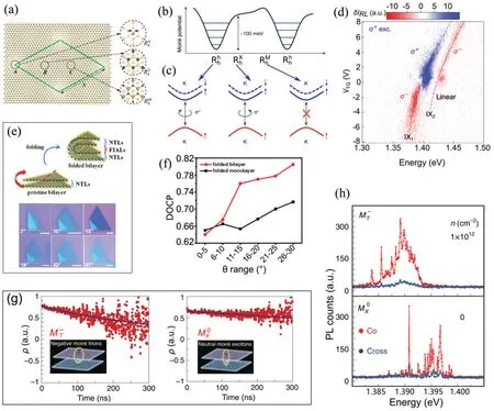
Fig.5.Valley polarization in moir′e superlattice.(a)Moir′e pattern in an MoX2/WX2 (X =S,Se)heterostructure.Three local atomic registriesof R-stacking withμsite of the MoX2 layer aligning with the hexagon center of WX2 layer.[74](b)The spatial variation of the moir′e potential and the constrained interlayer exciton resonances.(c)Optical selection rules of different atomic registries.[73](d)Polarization-resolved PL map.Net polarization ΔIRL =IR-IL as a function of the gate voltage VTG.IX1 and IX2 correspond to spin-conserving and spin-flip transitions,respectively.[58] (e) Fabrication process of one-interface-twisted multilayer MoS2 and the optical microscopy of folded bilayer MoS2 with different twist angles.(f)Twist angle dependence of DOCP in folded bilayer(red curve)and monolayer(black curve)MoS2.[77] (g)Decay of valley polarization for negative(M-T)and neutral(M0X)moir′e excitons in MoSe2/WSe2 moir′e superlattice heterostructure,with valley lifetime of about 370 ns and 1μs, respectively.(h)Helicity-resolved PL spectra for negative(M-T)and neutral(M0X)moir′e excitons in MoSe2/WSe2 moir′e superlattice heterostructure.[16] Figure reproduced with permission from (a) Ref.[74], AAAS; (b), (c) Ref.[73], Nature Publishing Group;(d)Ref.[58],Nature Publishing Group;(e),(f)Ref.[77],John Wiley and Sons;(g),(h)Ref.[16],Nature Publishing Group.
Moir′e pattern,including the moir′e periodicity and the superlattice potential, severely depends on the twist angle and lattice mismatch between two monolayers.Excitons exhibit tunable valley properties with variable twist angles.Valley polarization has been observed to be co-circularly polarized for 57°and 20°heterobilayers and cross-circularly polarized for 2°twist angle.[17]Zhanget al.[77]have systematically investigated twist angle dependent valley polarization evolution in multilayer moir′e supperlattics of MoS2with one twisted interface(Fig.5(e)).The DOCP was found to increase with enhanced rotation angle in both folded monolayer and bilayer MoS2(Fig.5(f)).The highest DOCP reaches a maximum value of above 70% near 30°in folded monolayer and 86%at 27°in folded bilayer.This result is higher than reported for twisted homobilayers, which is attributed to the strengthened dielectric screening effect from the self-encapsulation.The upward tendency of DOCP with twist angle was suggested to result from band mismatch.In specific, as twist angle increased, enlarged mismatch momentum led to a smaller transition dipole, suppressing the intervalley depolarization and achieving a longer valley lifetime.Since the positive correlation between valley lifetime and valley polarization is depicted by Eq.(2),increasing valley polarization is obtained.
In the presence of a moir′e pattern, free excitons are captured in the moir′e potential, termed moir′e excitons.Moir′e excitons were reported to exhibit an ultra-long lifetime.Mahdikhanysarvejahanyet al.[78]have observed moir′e exciton lifetime up to 300-800 ns in R-stacking (near 0°twisted) MoSe2/WSe2heterostructures.In H-stacking (near 60°twisted) MoSe2/WSe2moir′e superlattices,[16]valleypolarized lifetimes of 1 μs and 370 ns have been observed for moir′e excitons and moir′e trions, respectively, by means of electrostatic doping(Fig.5(g)).Analogously,Kimet al.[79]have revealed the negative circularly polarized emission of the single moir′e exciton and trion and observed the valley dynamic of moir′e trions lasting around 700 ns via the focus ion beam technique.This phenomenon is attributed to the participation of the moir′e dark trions, which are composed ofKKexciton and an excess electron from theQ-valley(I-valley)trapped in the moir′e potential.Apart from the long-lasting lifetime,giant valley polarizations up to 70%-100%have been reported in MoSe2/WSe2moir′e superlattices with 60°twist angle(Fig.5(h)),which were suggested to result from fast interlayer transfer together with long valley lifetime.[16,17,80,81]
3.4.Transport of valley polarization
Valleytronic devices based on vdW materials are promising for optical communication and information processing in integrated circuits.One prerequisite is that valley-polarized excitons possess a sizeable diffusion length,which requires a long exciton lifetime and valley-polarized lifetime.This is because of the proportional relation between the diffusion lengthLDand the valley lifetimeτ,which is described awhereDis the diffusion constant.Excitons in monolayer TMDs hold short valley lifetime, typically in picosecond order.In contrast, the valley lifetime of interlayer excitons is remarkably extended in TMD heterostructures due to the reduced e-h exchange interaction.In this part, we will discuss the diffusion of valley-polarized interlayer excitons in TMD heterostructures and the separation of valley-polarized excitons assisted by metasurfaces in monolayer and heterostructures.
3.4.1.Diffusion of valley-polarized interlayer excitons
Interlayer excitons are ideal candidates for valley information transport owing to their long valley-polarized lifetime.Riveraet al.[46]have determined a valley lifetime of 40 ns under a gate voltage of 60 V in MoSe2/WSe2heterostructures at 30 K.Such a long-lived polarization enables the visualization of the diffusion of valley-polarized excitons over micrometers.Figure 6(a) shows the evolution of valley polarization,which exhibits a ring with a diameter increasing with excitation intensity.This result can be explained by valleydependent many-body interactions in interlayer exciton gas of high density.Considering interlayer excitons possess out-ofplane dipoles, interlayer excitons experience mutually repulsive forces through dipole-dipole and exchange interactions.When the interlayer exciton density is high enough,an increasing expansion of valley polarization with excitation intensity can be observed away from the excitation spot.
The formation of moir′e pattern results in moir′e potential up to 100 meV,[74,75]which limits the diffusion of interlayer excitons.In response to this issue, Unucheket al.[82]introduced an atomically thin spacer layer of h-BN between the constituent monolayer of MoSe2/WSe2heterostructures,which effectively enhances the diffusion length of valleypolarized excitons.Furthermore,they realized a switch device that electrically operated the flow of valley-polarized excitons via multiple back gates.Valley-contrasting interlayer excitons were optically initialized byσ+circularly polarized light,and the emitted polarization for the off and on states are shown in Figs.6(b)and 6(c).Valley-polarized excitons were found to be capable of traveling an additional 1.3μm in the on state while being stopped before the control gate in the off state.The valley polarization switch could sustain up to a temperature of 100 K due to the large binding energy of interlayer excitons.
3.4.2.Separation of valley-polarized excitons
Building valleytronic devices calls for the separation of valley-polarized excitons.One strategy to accomplish this goal is to couple the TMD monolayer or heterostructures to plasmonic nanostructures, which can facilitate valley transport and establish an interface between valleytronic and photonic devices.Sunet al.[83]have designed an array of subwavelength asymmetric grooves (Fig.6(d)), which support chirality-dependent surface plasmon polariton(SPP)propagation along its side walls.By placing monolayer MoS2on top of this metasurface,spatial separation of the valley-polarized excitons was observed at room temperature(Fig.6(e)).This separation is enabled by the near-field coupling between excitons and guided surface plasmon polariton modes in the grooves.The spatial separation between valley excitons is determined to be about 1.2μm and the maximum valley polarization along the propagation is around 18%.This is a big improvement for monolayer TMDs, which commonly exhibit no valley polarization at room temperature.
The spatial separation of valley-polarized interlayer excitons has also been demonstrated in MoS2/WSe2heterostructures at room temperature.[48]The heterostructures are stacked on a silicon-on-insulator with a 220 nm thick silicon film on a 2 μm buried dioxide, as shown in Fig.6(f).The silicon film and heterostructures are suspended, which would induce strain and thus a potential gradient, leading to the appearance of the valley Hall effect.This speculation was experimentally verified.Figure 6(g) displays the spatially resolved polarized-dependent PL emission with dashed lines indicating the edge of individual monolayer.The interlayer excitons from two valleys propagate towards the sample edge and then are separated into two opposite transverse directions.The robust valley-polarized interlayer exciton transport at room temperature provides realistic possibilities for the development of opto-valleytronic devices based on TMD heterostructures.
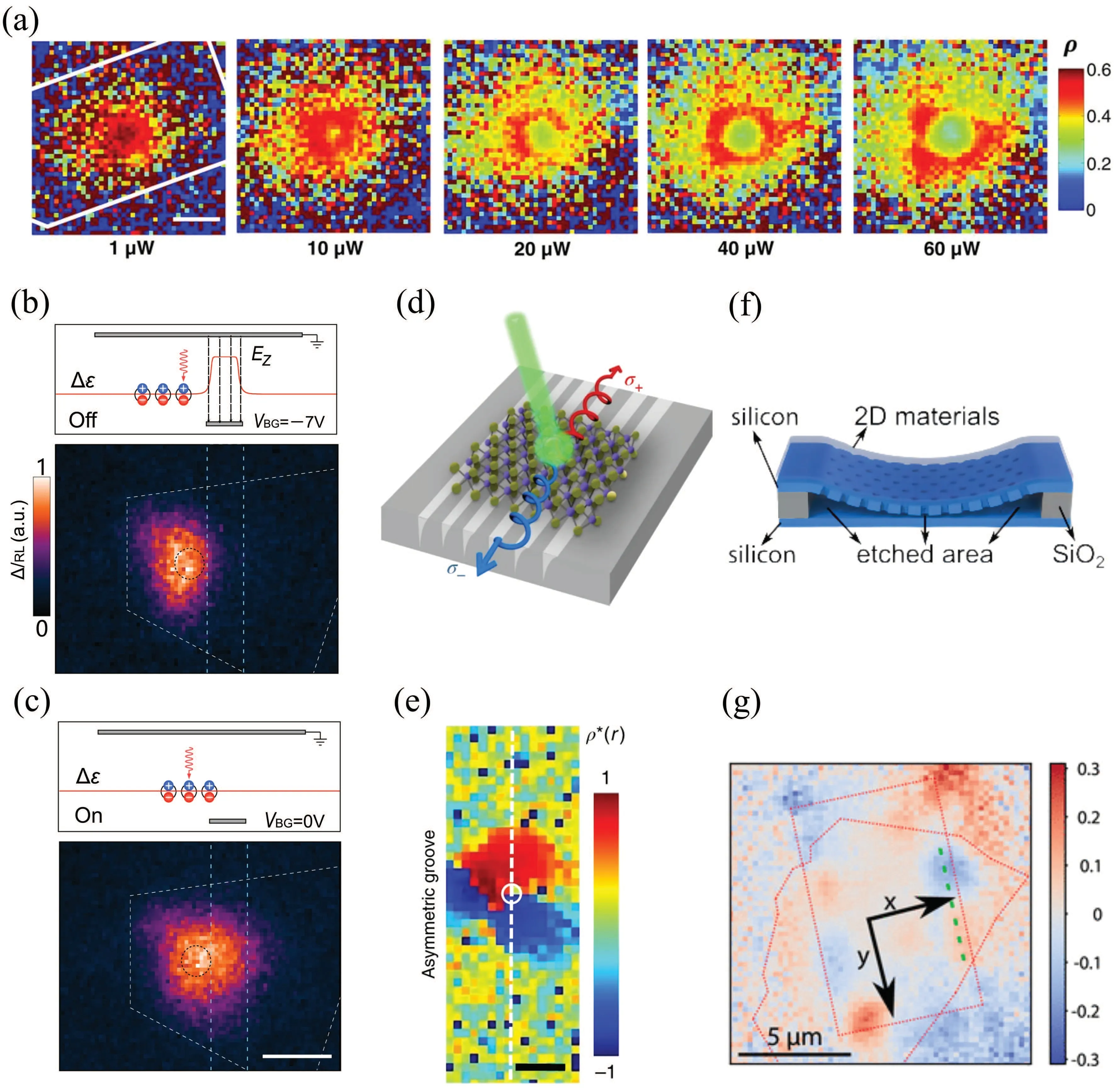
Fig.6.Transport of valley polarization.(a)Spatial map of valley polarization in MoSe2/WSe2 heterojunction under 1-60μW excitation.[46](b),(c)Energy profile in the off((b),VTG=0 V,VBG=-7 V)and on((c),VTG=0 V,VBG=0 V)states of the MoSe2/WSe2 excitonic transistor,and the corresponding maps of circular polarization ΔIRL.[82] (d)Schematic of valley excitons separation by attaching a MoS2 monolayer to a metasurface composed of subwavelength asymmetric grooves.(e) Color maps of valley polarization of (d).[83] (f) Structure of the silicon suspended slab,made of SOI material with 220 nm thick silicon layer(blue layer)on 2μm buried oxide(gray layer).(g)Spatial map of the degree of polarization in(f)structure at room temperature.The excitation spot serves as the origin for the x and y axes.Scale bar,2μm in(a),(c),(e),and 5μm in(g).[48] Figure reproduced with permission from(a)Ref.[46],AAAS;(b),(c)Ref.[82],Nature Publishing Group;(d),(e)Ref.[83],Nature Publishing Group;(f),(g)Ref.[48],American Chemical Society.
4.Valleytronic devices
Based on valley polarization, novel valleytronic devices have been designed and demonstrated.In this part,we briefly discuss the latest developments in the optoelectronic devices of valley LEDs and valleytronic transistors.
4.1.Valley LED
PN junction is the essential element for the fabrication of traditional LEDs,in which electrons and holes are injected into n-and p-doping regions under electric field,respectively,and then radiative recombination happens.For TMDs that have two isolated anisotropic valleys, the carrier distribution of electron-hole overlap in two valleys can be shifted by an in-plane electric field, which gives rise to circularly polarized luminescence.Consequently,valley LED is designed and demonstrated.
WSe2could display ambipolar conductivity under opposite gate voltages.Based on this unique characteristic,Zhanget al.[84]have designed and formed the p-i-n junction valley LED by using an electric-double-layer transistor(EDLT)structure with WSe2thin flake as the channel material(Fig.7(a)).Figure 7(b) shows the EL spectra in two opposite source-drain bias directions at 100 K.Circularly polarized luminescence from the specific valleys was observed.The circular polarization switches its sign when the bias is reversed.This electrical control of circularly polarized luminescence could be explained by the inset of Fig.7(b).The distribution of electrons and holes shifts in the opposite direction under an in-plane electric field.Then,the electron-hole overlap differs in two valleys due to anisotropic carrier distribution induced by trigonal wrapping.Valley overlap polarization gives rise to an intensity difference in luminescence from two valleys,resulting in circularly polarized luminescence.
Hereafter, Yanget al.[85]constructed a p+-Si/i-WS2/n-ITO heterojunction with monolayer WS2.They observed circularly polarized luminescence decreased as the forward bias increased, with a maximum polarization of 81%.This decreased tendency of valley polarization is mainly attributed to the rising intervalley scattering with the increasing doping.
Valley LEDs typically work at low temperature due to the exponential decay of temperature-dependent polarization induced by phonon-mediated intervalley scattering.Puet al.[86]realized a room-temperature chiral LED in monolayer WS2by introducing uniaxial strain to the device with a bending stage(Fig.7(c)).Figures 7(d) and 7(e) show the valley-polarized EL from the strained and unstrained regions under forward and reverse source-drain bias, respectively.Chiral EL was only observed in strained areas at room temperature.Besides,the intensity difference betweenσ+andσ-flips when the inplane electric field is inverted,indicating the electrical control of room-temperature valley-polarized EL in strained WS2valley LED.These results were interpreted by strain-induced giant valley drifts and electric-field-induced Fermi pocket deviations in+Kand-Kvalleys.This work provides a new route for practical valley LEDs based on monolayer TMD semiconductors.

Fig.7.Valley LEDs.(a) Device structure of TMD electric-double-layer transistor (EDLT) with WSe2 thin flake as the channel material.(b) Circularly polarized EL spectra of (a) for two opposite current directions at 100 K.Inset: schematic of electron and hole distributions shifted by the built-in electric fields Ebi.[84] (c) Optical setup to measure the EL polarization of chiral LED based on strained WS2 at room temperature.The emitted circularly polarized light passes through λ/4,linear polarizer,finally enters a Si photodiode and is collected as the photocurrent Iph.(d),(e)Integrated Iph for σ+and σ-polarized emission detected in both flat(middle)and bent(bottom)conditions with a bias of+3.3 V(d)and-3.3 V(e).The shaded area shows the dark currents,which originate from background photocurrents.[86]Figure reproduced with permission from(a),(b)Ref.[84],AAAS;(c)-(e)Ref.[86],John Wiley and Sons.
4.2.Valleytronic transistor
Broken inversion symmetry induces out-of-plane Berry curvatures with opposite signs in +Kand-Kvalleys.Berry curvature is analogous to a magnetic field in moment space,[10]which allows the electrical transport to exhibit valley-contrasting performance.One example is the valley Hall effect (VHE) shown in Fig.8(a).Carriers from opposite valleys (+Kand-K) obtain an anomalous velocity and move towards two opposite transverse directions in the presence of the in-plane electric field.Transistors based on VHE have been developed.
The first experimental work was reported in monolayer MoS2at 77 K.[87]By preferentially exciting electrons into a specific valley with circularly polarized light on resonance with A exciton of MoS2monolayer,valley Hall voltage is detected.Figure 8(b)shows the valley Hall voltage as a function of the bias voltage applied along the short channel.The linear dependence under right-to-left(R-L)or L-R modulated circularly polarized excitation indicates a photoinduced anomalous Hall effect driven by a net valley polarization.The sign of the hall voltage is reversed when the excitation is changed to LR modulation, revealing its helicity-dependent characteristic.Hall voltage is absent when replacing the excitation with linear polarized light(s-p)or changing the sample with a bilayer device due to the inversion symmetry.
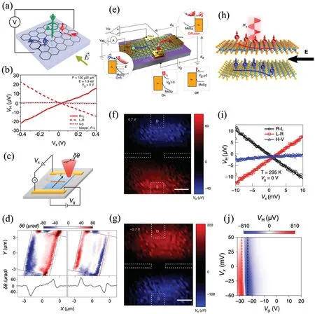
Fig.8.Valleytronic transistor.(a)Schematic of valley Hall effect(VHE).(b)The source-drain bias(Vx)dependence of the Hall voltage(VH)for the monolayer MoS2 device under R-L (red solid line), L-R (red dashed line), and half-wave s-p modulations (red dotted line).Result from the bilayer device under R-L modulation(blue solid line)is also shown.[87] (c)Diagram of the measurement of bilayer MoS2 field effect transistor.(d) Spatial map and selected horizontal linecut of the Kerr rotation angle δθ under gate voltage Vg =20 V (left panel) and -5 V(right panel).Black dashed lines show the boundaries of the channel.[88] (e)Schematics and operation mechanism of a valleytronic transistor composed of a standard MoS2 transistor, two lateral Hall probes and a purposely aligned chiral plasmonic antennae array. Ex and Ez denote Vsd and Vg,respectively.(f),(g)Valley Hall voltage mappings of device(e)under Vsd =0.7 V(f)and-0.7 V(g).[89] The white dashed lines display the edges of the metallic electrodes.Scale bar,4μm.(h)Illustration of VHE in the MoS2/WSe2 heterostructure.In-plane electric field E and carrier layer-separation-induced valley and layer-dependent anomalous velocity.(i)VHE based on the MoS2/WSe2 heterostructure at room temperature.(j)VH as a function of Vx and Vg.[90]Figure reproduced with permission from(b)Ref.[87],AAAS;(c),(d)Ref.[88],Nature Publishing Group;(e)-(g)Ref.[89],Nature Publishing Group;(h)-(j)Ref.[90],Nature Publishing Group.
In order to break the inversion symmetry in bilayer TMD and produce the VHE, the same research group realized the VHE transistor based on bilayer MoS2by applying gate voltage(Fig.8(c)).[88]By Kerr rotation microscopy detection,the valley polarization induced by the longitudinal electrical current was observed to be present only near the two edges of the device channel with opposite sign(Fig.8(d)), which is a signature of the VHE.In addition, it was demonstrated that the valley polarization accumulated near the edge can be modulated by the gate voltage,indicating the electrical tunability of VHE.
The VHE transistors in the above two reports can only work at cryogenic temperature.Liet al.[89]demonstrated a VHE device operating at room temperature by decorating monolayer MoS2with asymmetric ends of the plasmonic antennae to the source and drain electrodes (Fig.8(e)).This alignment could selectively generate valley-polarized carriers,give rise to opposite valley polarization between source and drain pumping,and result in the anomalous Hall voltage at the contact interface as a manifestation of the VHE(Figs.8(f)and 8(g)).They also revealed gating manipulation of the magnitude of the valley Hall voltage.
VHE transistors operating either at cryogenic temperatures[87,88]or via plasmonic structures[89]limit their practical application.Our research group reported the observation of the VHE at room temperature in MoS2/WSe2heterostructures (Fig.8(h)), which is depicted by the linear dependence of the valley Hall voltage on the channel bias under R-L (L-R) modulated circularly polarized excitation(Fig.8(i)).[90]Besides, both the polarity and magnitude of VHE are gate tunable (Fig.8(j)).This result is in stark contrast with VHE in MoS2monolayer,where only the magnitude is tunable.[87,88]We discussed the bipolar nature of the VHE mechanism and suggested that the combined action of the bipolar nature of carrier transport and electrically induced valley-dependent band shift in the heterostructure created the bipolar valleytronic transistor.
5.Conclusion and perspectives
In this review, we have systematically summarized the recent advances in valley polarization in nonmagnetic TMD layered semiconductors, including the initial generation, relaxation, manipulation, and transport of valley polarization,which are closely related to the information processing based on the valley degree of freedom.As for the generation of valley polarization, there are two typical approaches, optical pumping with circularly polarized light and electrical injection of spin-polarized carriers, both of which are based on the strong SOC induced spin-valley coupling in TMD materials.In the case of the relaxation of valley polarization, TMD heterostructures possess long-lasting valley polarization decay time in contrast to TMD monolayer owing to the weakened electron-hole exchange interaction.In view of the manipulation of valley polarization, a variety of strategies have been developed, and we mainly discuss the external electrical gating,magnetic field and magnetic proximity effect,and internal moir′e pattern.Progress on the transport of valley information is also discussed from the perspective of diffusion and separation of valley polarization.Finally,we discuss the development of two typical valley optoelectronic devices,valley LEDs and valley Hall transistors.
Although significant progress has been achieved in improving valley polarization,this field is still in its infancy and faces many challenges and obstacles.On the one hand,robust valley polarization still needs to be demonstrated,especially at room temperature.Valley polarization is currently mostly between 30%and 80%, but primarily at low temperatures.The valley polarization decreases dramatically as the temperature increases due to strengthened intervalley scattering.Although plasmonic structures or exerting a magnetic field can effectively enhance the valley polarization, their practical application is limited.Electrical generation through spin injection via ferromagnetic semiconductors or metals is proposed to be efficient,but it is still at a relatively preliminary conceptual level and is hindered by the imperfect interface.On the other hand,the transport of valley polarization still needs to be prolonged.Strategies to drive excitons and valley polarization dynamics are desirable and should be further exploited.Improved single crystal growth and upgraded device processing are required,which serve as building blocks for future valleytronic devices.Although valleytronics is still at the level of novel physics phenomenon and needs more efforts to be developed as a technology element, this field opens up a new direction in future information processing and storage.
Acknowledgements
C.Y.J.acknowledges the Key Laboratory of Photoelectronic Thin Film Devices and Technology of Tianjin and the Engineering Research Center of Thin Film Optoelectronics Technology,Ministry of Education of China.
Project supported by the National Key Research and Development Program of China(Grant No.2022YFB2803900),the National Natural Science Foundation of China (Grant Nos.61704121 and 61974075), Natural Science Foundation of Tianjin City (Grant Nos.19JCQNJC00700 and 22JCZDJC00460),Tianjin Municipal Education Commission(Grant No.2019KJ028),and Fundamental Research Funds for the Central Universities(Grant No.22JCZDJC00460).
猜你喜歡
音樂天地(音樂創(chuàng)作版)(2023年5期)2023-09-25 02:45:16
樂山師范學(xué)院學(xué)報(2022年10期)2022-11-25 05:36:52
大眾文藝(2022年21期)2022-11-16 14:21:20
青年文學(xué)家(2021年29期)2021-11-19 16:11:47
中老年保健(2021年12期)2021-08-24 03:30:16
金秋(2021年24期)2021-04-01 10:05:42
金橋(2021年2期)2021-03-19 08:34:26
青年生活(2020年5期)2020-03-27 14:29:00
金秋(2019年24期)2019-06-17 11:30:58
中國農(nóng)資(2019年2期)2019-01-15 08:40:58
- Chinese Physics B的其它文章
- Corrigendum to“Reactive oxygen species in plasma against E.coli cells survival rate”
- Dynamic decision and its complex dynamics analysis of low-carbon supply chain considering risk-aversion under carbon tax policy
- Fully relativistic many-body perturbation energies,transition properties,and lifetimes of lithium-like iron Fe XXIV
- Measurement of the relative neutron sensitivity curve of a LaBr3(Ce)scintillator based on the CSNS Back-n white neutron source
- Kinesin-microtubule interaction reveals the mechanism of kinesin-1 for discriminating the binding site on microtubule
- Multilevel optoelectronic hybrid memory based on N-doped Ge2Sb2Te5 film with low resistance drift and ultrafast speed