
A field-effect WSe2/Si heterojunction diode
2023-02-20 13:16:42RuiYu余睿ZheSheng盛喆WennanHu胡文楠YueWang王越JianguoDong董建國HaoranSun孫浩然ZengguangCheng程增光andZengxingZhang張增星
Chinese Physics B 2023年1期
Rui Yu(余睿), Zhe Sheng(盛喆), Wennan Hu(胡文楠), Yue Wang(王越), Jianguo Dong(董建國),Haoran Sun(孫浩然), Zengguang Cheng(程增光), and Zengxing Zhang(張增星),2,?
1State Key Laboratory of ASIC and System,School of Microelectronics,Fudan University,Shanghai 200433,China
2National Integrated Circuit Innovation Center,Shanghai 201203,China
Keywords: two-dimensional material,ambipolar semiconductor,field-effect transistor,optoelectronic device
1. Introduction
In the past decades, silicon-based devices have been extensively developed and applied, which has promoted the development of semiconductor technology. However, with the rapid growth of information technology,especially the internet of things (IoTs), enormous information needs to be acquired and processed, putting forward urgent demand for devices with high performance and high energy efficiency. Therefore,it has become an emergent field to explore new materials and new physical properties, and thus to develop new principle devices and new computing architectures.[1]Recently,two-dimensional(2D)materials have attracted tremendous attention due to their ultrathin structure and excellent physical properties,[2–5]which have been widely proposed for excellent electronic and optoelectronic devices.[6–9]Among these 2D materials,ambipolar 2D semiconductors,[10–12]like WSe2,are receiving especial interest,in which the major charge carriers can be dynamically tuned by controlling the electrical field. Based on such characteristic,various field-effect diodes have been reported,[13–18]in which the electronic and optoelectronic properties can be modulated by a gate voltage.They thus have potentials for logic optoelectronic devices[19,20]or neuromorphic optoelectronic devices[21]for ultrafast image sensors by implementing the artificial neural network(ANN)algorithm[22]to perform the in-sensor computing circuits.
Although the ambipolar 2D semiconductor based fieldeffect diodes have shown great potential, it is expected that silicon-based devices will still be the mainstream of semiconductor technology in the near future with the advantages of mature technology and low cost. Therefore, it is significant to integrate 2D materials into Si to develop a heterogeneous integration technology so it can make full use of the superiorities of Si and 2D materials. To this end, there have been some reports which tried 2D-materials/Si heterojunction devices that exhibited excellent properties in electronics and optoelectronics,such as graphene/Si,[23,24]MoS2/Si[25,26]and WS2/Si.[27,28]However, so far, few works have been carried out to push forward the field-effect diodes based on heterogeneous 2D ambipolar semiconductor and Si. In addition, the often-used bulk Si in these reported heterogeneous devices is not conductive for device isolation and integration.[29]Here,we demonstrate a field-effect heterojunction diode,where the channel is ambipolar-WSe2/Si heterojunction and the Si is from Si on insulator(SOI)that is conductive for device insolation and large-scale integration. The investigation indicates that the device exhibits a diode behavior with gate-modulated electronic and optoelectronic properties,indicating that it has potential as logic optoelectronic devices and neuromorphic optoelectronic devices for in-sensor computing circuits.
2. Result and discussion
Figure 1(a) illustrates the schematic configuration of the field-effect WSe2/Si heterojunction diode, in which the ntype Si and p-type WSe2heterojunction serves as the channel,hexagonal boron nitride (h-BN) and graphene (Gr) as the dielectric and gate electrode, respectively. All of the materials are assembled via van der Waals force interaction. In a typical fabrication process,a SOI wafer was used to obtain the bottom Si sheet. The thickness of the device layer is 100 nm and the resistivity is 0.005 Ω·cm. The Si sheet with a length of 15 μm and a width of 10 μm was firstly defined by e-beam lithography (EBL) and etched by inductively coupled plasma (ICP).And then metal electrodes(30 nm Au)were patterned on the Si sheet and around.After that,WSe2,h-BN and Gr flake were transferred and stacked on the specific positions layer by layer,all of which were mechanically exfoliated from bulk crystals.The details of the fabrication process can be seen in the supplementary material. Figure 1(b)shows an optical microscope image of a typical fabricated field-effect WSe2/Si heterojunction diode. The boundaries of each component are marked by solid lines with different colors and the area of the heterojunction region is around 44 μm2. Atomic force microscopy(AFM)was employed to determine the thickness of the flakes.As demonstrated in Fig. S2, the thicknesses of the Gr, h-BN and WSe2are 7 nm, 16.5 nm and 6 nm, respectively, indicating all of which are few-layer structures. Compared with 2D-material/Si heterojunctions using bulk silicon, our device based on the SOI technology enables the mutual isolation between devices, which should be feasible to realize the largearea on-chip integration in the future.

Fig.1. (a) Schematic device structure of the field-effect WSe2/Si heterojunction diode. (b)Optical microscope image of a typical fabricated device.
In our device,the contact between the Au electrodes and the WSe2is formed by transferring the 2D flake to the predeposited metal electrodes. Compared with directly depositing metal to 2D materials, such technique can reduce damages to the surface of the 2D materials and form a Van der Waals contact.[30,31]Figure 2(a)is theId–Vdscurves across the WSe2with various gate voltages(Vg)applied on the electrode E5, in which the drain/source voltage (Vds) is applied on the electrode E1 (drain) and E2 (source), as indicated in Fig. 1.It can be seen that the current (Id) is nearly linearly dependent on theVdsand the linear relationship of theId–Vdscurves is hardly affected by the gate voltagesVg, indicating that the Au/WSe2contact is close to ohmic. The Si/Au contact is studied with the electrode E3 (drain) and E4 (source). As shown in Fig. 2(b), theId–Vdscurve of the Si sheet is obviously linear with a high current at the level of 10-3A at 1 V, indicating that a high quality ohmic contact is formed between the Au and the Si sheet. Figure 2(c) shows theId–Vdscurve across the WSe2/Si heterojunction tested by applying voltages on the electrode E1 (drain) and E4 (source) with the top Gr gate open. The heterojunction exhibits an obvious rectifying behavior of p–n diode. WithVdsof-2 V and 2 V, the currentIdis-2.6×10⁻⁶A/cm2and 7.8×10⁻⁴A/cm2, respectively, demonstrating a rectifying ratio of~300. As both of the Au/WSe2and the Au/Si are nearly ohmic contacts, such rectification is reasonable to be ascribed to the WSe2/Si interface. From the slope of the curve,it can be extracted that the ideality factor(n)is about 1.37(detailed calculation method is shown in the supplementary material). The ideality factor is described asn=e/kT×dV/d(lnI), whereeis the electron charge,kis the Boltzmann constant,Tis the temperature,Vis the voltage andIrepresents the current.According to the Sah–Noyce–Shockley theory,[32]nis the parameter that reflects the current transport mechanism in p–n diodes. Whennis close to 1,the current is dominated by the diffusion effect. While it is close to 2,it is ascribed to the recombination effect.Thenhere is close to 1,indicating that the transport should be dominated by the diffusion rather than the recombination mechanism.
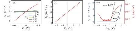
Fig.2. (a) The Id–Vds curves across the WSe2 at different Vg. (b) Id–Vds curve across the Si sheet. (c) Id–Vds curve across the WSe2/Si heterojunction,in which the blue is in linear scale and the red is in logarithmic.
An important application of p-n diodes is for photodetectors. We studied the optoelectronic properties of the WSe2/Si heterojunction diode and the results are shown in Fig. 3. As shown in Fig. 3(a), an obvious photocurrent is generated under the light illumination and it increases with the increase of the light power density (P). Here the photocurrent is defined asIph=Ilight-Idark, whereIlightis the current density under light illumination andIdarkis the current density in dark. For the light power densityP, we used an optical power meter to measure the power(Q)of the incident light;Pwas calculated by dividingQwith the light spot area. For the current densityIlightandIdark,we extracted the currents from theI–Vcurves of the WSe2/Si heterojunction at a certainVdsunder light illumination and dark,respectively;the current densities were calculated by dividing the currents with the junction area(overlapping area of the WSe2and Si,44 μm2). The p–n diodes often work at the reverse bias voltage state when used for photodetectors. To obtain the optimal work voltage of the WSe2/Si heterojunction diode,theIph–VdsandRT–Vdscurves are measured under the light power density of 2.66 mW/cm2, whereRTis defined asIph/Idark.As shown in Fig.3(b),the photocurrent is generated under both positive and negative bias ofVds,andRTreaches the maximum of 103atVds=-1.2 V.Generally,IphandRTshould be as large as possible for photodetectors.Therefore,Vds=-1.2 V should be the optimal work voltage for our device at such situation. In the following,Iphdependent on light power density(P)is studied atVds=-1.2 V unless other stated. As presented in Fig.3(c),theIph–Pcurve is roughly linearly, which is benefit for photodetection. For photodetectors,some specific indicators are often used to characterize their performance, like response time, photo-switch property,stability,responsivity(R),detectivity(D*)and external quantum efficiency(EQE).Rrepresents the ability of photoelectric conversion of photodetectors,which is described asR=Iph/P.D*represents the detection ability of photodetectors and it is described asD*=R/(2eIdark)1/2,whereeis the electron charge. EQE represents the ability of photodetectors to transform the photonic signal into an electrical signal and it is determined by the equation EQE=Rhc/eλ,wherehis the Planck constant,cis the light speed andλis the wavelength of the incident light. Our experimental results reveal that the device has good response time with rise time(tr)of 0.13 ms and fall time(tf)of 5.55 ms,as shown in Fig.3(d),which were obtained via measuring the time with the current rising(falling)from 10%(90%)to 90%(10%). The WSe2/Si heterojunction diode also possesses a pretty good photo-switch property and stability with a test time more than 1000 s(Fig.3(e)). As presented in Fig. S3,RandD*of the heterojunction diode are 0.045 A/W and 4.5×10¹⁰Jones, respectively. Meanwhile,the maximum EQE is calculated to be 8.9%. A comparison of our device with other reported photodetectors based on 2Dmaterial/Si heterojunction is shown in Table 1.It demonstrates that our device is competitive in main performances. In addition, we also studied the photoresponse of our device to the light with different wavelengths; all of them were measured with a power density of 2.66 mW/cm2atVds=-1.2 V. As shown in Fig.3(f),the responsivity of the device is dependent on the light wavelength. When the light is of 805 nm, the photoresponse decreases obviously. For the 1045 nm incident light,it is difficult to observe the responsivity.

Fig.3. (a)The Id–Vds curves across the WSe2/Si heterojunction diode under light illumination with different power densities. (b)The corresponding Iph–Vds and RT–Vds curves of the WSe2/Si heterojunction diode. (c)Scatting points of Iph dependent on the light power density P. (d)Response time(rise: tr, fall: tf) and (e) photo-switch property of the WSe2/Si heterojunction diode. (f) Scatting points of responsivity (R) dependent on the light wavelength. Data from(a)to(e)were all acquired with the light of 638 nm,data from(b)to(f)were all at P=2.66 mW/cm2,and data from(c)to(f)were all at Vds=-1.2 V.
Table 1. Performance comparison of our device with reported 2D-material/Si heterostructured photodetectors.
As reported,the optoelectronic properties of the ambipolar 2D semiconductor based devices can be modulated by an electrical field. Such behavior can be used for logic optoelectronic devices and neuromorphic optoelectronic devices for in-sensor computing circuits, which has been attracting great attention recently. Therefore,it is significant to study the gate-modulated properties of the heterojunction diode. Figure 4(a) shows theId–Vdscurves of the WSe2/Si heterojunction diode withVgopen, 5 V and-5 V respectively, and the electrodes E1, E4 and E5 serve as the drain, source and gate,respectively. As shown in the curves, whenVg=5 V is applied on the Gr gate, it can be obtained that the currentIdis-8.35×10⁻⁴A/cm2atVds=-2 V and 3.17×10⁻⁶A/cm2atVds=2 V,respectively,with a rectifying ratio of~263. Compared with theVgopen, the rectifying direction is reversed.WhenVg=-5 V is applied, the heterojunction is of similar rectifying direction like that ofVgopen. The currentIdis-1.30×10⁻⁵A/cm2atVds=-2 V and 1.61×10⁻³A/cm2atVds=2 V with a rectifying ratio of 124.That is to say,the gate voltage can modulate the heterojunction,including the rectifying ratio and direction. To confirm this modulation,the transfer characteristic curves of the heterojunction atVds=-2 V and 2 V were measured and shown in Fig.4(b). The diagram is divided into two regions (region I and region II) by the intersection of the two curves at the position ofVg= 1 V. The current atVds=2 V is larger than that atVds=-2 V in region I but smaller in region II,further proving that the diode is indeed modulated when the gate voltage varies from-5 V to 5 V,and the modulation is continuous.
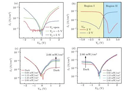
Fig.4. (a) The Id–Vds curves of the field-effect WSe2/Si heterojunction diode with Vg open, 5 V and-5 V respectively. (b)Id–Vg curves of the heterojunction with Vds of -2 V and 2 V, respectively. Id–Vds curves of the heterojunction under light illumination with different power densities at(c)Vg=5 V and(d)Vg=-5 V,respectively.
Figures 4(c) and 4(d) show the optoelectronic properties of the diode at different gate voltages under 638 nm light illumination. With the similar method as discussed above, we can get that the optimal work voltageVdsof 1 V forVg=5 V,and the maximum values ofR,D*and EQE are 0.122 A/W,1.2×1011Jones and 24.1%, respectively (Fig. S4). ForVg=-5 V,the optimal work voltageVdsis-1 V,and the maximum values ofR,D*and EQE are 0.044 A/W,1.33×1010Jones and 8.7%,respectively(Fig.S5).Compared withVgopen,these indicate that the optoelectronic behavior of the field-effect diode can be modulated by the gate voltage,exhibiting that it can be used for logic optoelectronic device and neuromorphic optoelectronic devices.
To well understand the field-effect WSe2/Si heterojunction diode,we further studied the gate-modulated mechanism.Figure 5(a)shows the transfer characteristic curve of the WSe2FET,where the drain/source and gate electrode are E1/E2 and E5, respectively. The curve with a valley shape demonstrates that it is a typical ambipolar FET. When the gate voltage is scanned from-5 V to 5 V,the current first decreases and then increases. The neutral point is a little bigger than 0 V,indicating that the WSe2is a little p-doped. We also studied the gateeffect on the Si sheet,where E3/E4 and E5 electrode serve as the source/drain and gate electrode, respectively. The result exhibits that the Si sheet is nearly not affected by the Gr gate probably due to the low resistivity of the Si (Fig. S6). Based on such fact,the band diagrams of the WSe2/Si heterojunction at different gate voltages are shown in Figs.5(b)–5(d). As for the few-layer 2D WSe2,the electron affinity is~4.06 eV and the bandgap is~1.31 eV.[36]The Si has the electron affinity of 4.05 eV and the bandgap of 1.12 eV.When the heterojunction is formed,electrons(holes)in the n-type Si(p-type WSe2)diffuse into the p-type WSe2(n-type Si)due to the difference of charge carrier concentration,bending down(up)the energy band of WSe2(Si)close to the interface,initiating a depletion region and making the heterojunction as a p–n diode with a built-in electrical field(Fig.5(b)). WhileVg=5 V is applied,electrons are highly doped in the WSe2and the Si sheet is not affected, leading to that electrons diffuse from the WSe2to the Si,making the heterojunction as an n+–n diode with a reversed rectifying direction(Fig.5(c)). WhenVg=-5 V is applied,similarly,more holes are accumulated in the WSe2,and the heterojunction finally becomes a p+–n diode due to the difference of carrier concentration (Fig. 5(d)). For the photoresponse, while light is illuminated on the heterojunction,the photons can be absorbed by both WSe2and Si due to that the light can be transmitted through the very thin WSe2. The absorbed photons generate photo-excited charge carriers that are then separated by the built-in electrical field in the heterojunction and the photocurrent is present. As we all know, a reverse bias voltage can strengthen the built-in electric field in the p–n diode,leading to the increase of the photoresponse in the reverse bias condition. Therefore, in our experiment we used a reverse bias voltage to strengthen the photoresponse. It should be noted in Fig. 3(f) that the photoresponse decreases obviously for the light of 805 nm and almost disappears for 1045 nm,which should be due to the decrease of the absorbed photons since they are consistent to the light absorption characteristics of the WSe2and Si.[33,37]
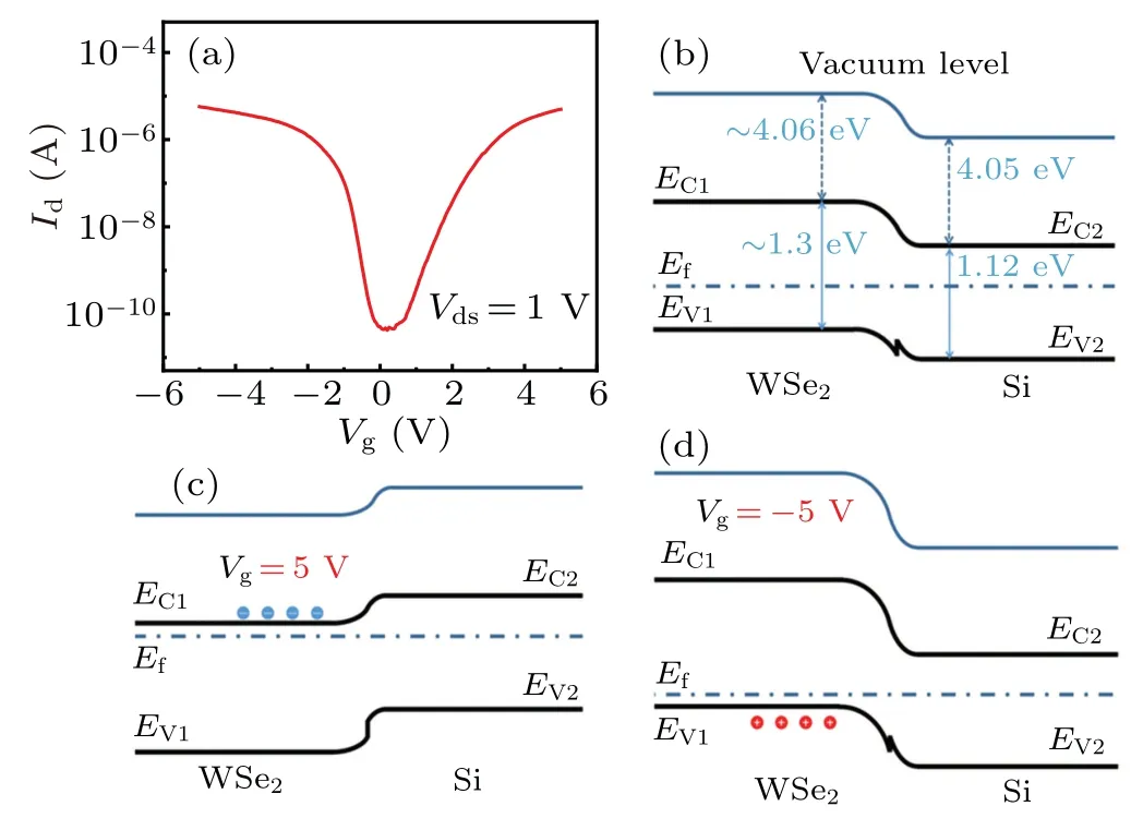
Fig.5. (a) Transfer characteristic curve of the ambipolar WSe2 FET.Band diagram of the WSe2/Si heterojunction diode with gate voltage of(b)open,(c)5 V and(d)-5 V,respectively.
3. Conclusion
We reported a field-effect WSe2/Si heterojunction diode by adopting the 2D WSe2and the device layer of SOI. In terms of electrical properties,the heterojunction exhibits a p–n diode behavior with a rectifying ratio of~300 and an ideality factor of 1.37. As a photodetector, the heterojunction has optoelectronic properties with response time of 0.13 ms,Rof 0.045 A/W,D*of 4.5×10¹⁰Jones and EQE of 8.9%.Due to the ambipolar characteristic of the WSe2, the heterojunction can be modulated among p–n, n+–n and p+–n diode by controlling the gate voltage, accompanied by the modulation of electrical and optoelectronic properties. WithVg=5 V, the heterojunction exhibits an n+–n diode behavior withR,D*and EQE tuned up to 0.122 A/W, 1.2×10¹¹Jones and 24.1%,respectively. WhileVg=-5 V,the heterojunction exhibits a p+–n diode behavior withR,D*and EQE of 0.044 A/W, 1.33×10¹⁰Jones and 8.7%, respectively. Our field-effect WSe2/Si heterojunction diode with gate tunable properties should be applicable as logic optoelectronic devices and neuromorphic optoelectronic devices for in-sensor computing circuits. In addition, the SOI wafer used here makes the device more easily isolated and integrated,which may enable large-scale integration and be more suitable for integrated circuits and image sensors.
Data availability statement
The data that support the findings of this study are openly available in Science Data Bank at http://doi.org/10.57760/sciencedb.j00113.00055.
Acknowledgements
Project supported by the Ministry of Science and Technology of China(Grant No.2018YFE0118300),the National Key Research and Development Program of China (Grant No. 2018YFA0703703), and State Key Laboratory of ASIC& System (Grant No. 2021MS003), and Science and Technology Commission of Shanghai Municipality, China (Grant No.20501130100).
猜你喜歡
Chinese Physics B(2023年12期)2023-12-15 11:48:20
大眾文藝(2023年3期)2023-03-03 03:30:50
大眾文藝(2023年3期)2023-03-03 03:30:44
好孩子畫報(2022年6期)2022-12-01 07:10:30
好孩子畫報(2022年5期)2022-06-06 21:29:20
Chinese Physics B(2021年3期)2021-03-19 03:20:52
藝術(shù)評鑒(2020年2期)2020-03-23 13:34:24
Communications in Theoretical Physics(2018年10期)2018-11-24 07:40:02
世紀人物(2017年8期)2017-08-07 07:40:04
知音·上半月(2017年3期)2017-03-16 16:52:50
- Chinese Physics B的其它文章
- LAMOST medium-resolution spectroscopic survey of binarity and exotic star(LAMOST-MRS-B):Observation strategy and target selection
- Vertex centrality of complex networks based on joint nonnegative matrix factorization and graph embedding
- A novel lattice model integrating the cooperative deviation of density and optimal flux under V2X environment
- Effect of a static pedestrian as an exit obstacle on evacuation
- Chiral lateral optical force near plasmonic ring induced by Laguerre–Gaussian beam
- Adsorption dynamics of double-stranded DNA on a graphene oxide surface with both large unoxidized and oxidized regions