
Interfacial defect engineering and photocatalysis properties of hBN/MX2(M =Mo,W,and X =S,Se)heterostructures
2022-06-29 08:56:10ZhiHaiSun孫志海JiaXiLiu劉佳溪YingZhang張穎ZiYuanLi李子源LeYuPeng彭樂宇PengRuHuang黃鵬儒YongJinZou鄒勇進(jìn)FenXu徐芬andLiXianSun孫立賢
Chinese Physics B 2022年6期
Zhi-Hai Sun(孫志海), Jia-Xi Liu(劉佳溪), Ying Zhang(張穎), Zi-Yuan Li(李子源),Le-Yu Peng(彭樂宇), Peng-Ru Huang(黃鵬儒), Yong-Jin Zou(鄒勇進(jìn)),Fen Xu(徐芬), and Li-Xian Sun(孫立賢)
School of Material Science and Engineering,Guilin University of Electronic Technology,Guangxi Key Laboratory of Information Materials,Guangxi Collaborative Innovation Center of Structure and Property for New Energy and Materials,Guilin 541004,China
Keywords: hBN/MX2 heterostructures,interfacial defect,electronic state,photocatalytic properties
1. Introduction
Two-dimensional(2D)materials have attracted intensive research interest since the discovery of graphene,in which excellent photoelectric, thermoelectric, mechanical, and chemical properties have been reported, making these materials ideal candidates for new-generation nanoscale devices.[1–6]Most of the 2D materials, including hexagonal boron nitride(hBN),[7]transition metal dichalcogenides(TMDCs),[8]black phosphorus (BP),[9]layered double hydroxides (LDHs),[10]antimonene,[11]and germanene,[12]can be prepared by the methods such as mechanical exfoliation[13]and chemical vapor deposition (CVD).[14]For two decades of investigations,extensive efforts have been devoted to tailoring 2D materials to meet the desired properties for practical applications. One of the most popular strategies is to stack different 2D components together to form heterostructures of different functionalities, and has open up a new paradigm of interface engineering.[15,16]
When two 2D materials are vertically stacked together,owing to the work function differences and charge transfer,the band alignment at the interface will be modified. For instance, Denget al.[17]reported that the Schottky barrier height (SBH) of graphene/g-GaN heterostructures are effectively turned by controlling the interlayer distance. Sunet al.[18]developed a method of tuning the electrical characteristics of graphene/WSe2heterostructures through changing the interlayer coupling and a perpendicular electric field. In addtion, the physicochemical properties of heterostructures can be changed when defects exist in the interface. Fanget al.[19]demonstrated that interfacial defects give rise to a significant influence on the electronic states of AlN/MoS2heterostructures, in which different types of vacancies and dopants have different effects on the band arrangement and magnetic properties modifications. Zhaoet al.[20]found that the heptazine/triazine based g-C3N4heterostructure with the(F, Ti) co-doped interface can not only improve visible light absorption, but also promote electron–hole pairs separation and inhibit carrier recombination. Xuet al.[21]designed a Ztype photocatalyst (hBN/g-C3N4) through interfacial defectengineereing and revealed the effects of different defects on the interface of hBN/g-C3N4heterostructures. All these studies highlight the important role of interfacial defect engineering in developing of efficient novel nanoscale devices.
Here in this work, We construct a heterostructure composed ofMX2(M=Mo,W,andX=S,Se)and hBN,and investigate the influences of interfacial defects on the electronic structures and photocatalytic properties of heterostructures in detail by using density functional theory calculations. The results exhibit that interfacial defect engineering can not only change the band aligment of heterostructures but also control the types of photocatalysts,thereby providing a detailed guidance of design the new photocatalysts.
2. Computational methods
In this work,all calculations are performed using the Viennaab initiosimulation package(VASP),which is based on density functional theory(DFT)in a plane-wave basis set with the projector augmented wave (PAW) method.[22–24]The exchange correlation functional is approximated by the generalized gradient approximation of Perdew, Burke, and Ernzerhof(GGA-PBE).[25]The DFT-D3 in the Grimme approach is adopted since the GGA for exchange and correlation fails to explain the interaction between the layered structures.[26]In all calculations spin-polarization is taken into account. After the convergence test,the energy cutoff for plane-wave expansion is set to be 500 eV and aK-mesh to be 11×11×1 within the Brillouin zone. The energy convergence value of the Kohn–Sham equation using the self-consistent loop is set to be 1×10⁻⁵eV/atom, and the maximum stress is controlled to be within 0.01 eV/°A. To avoid the interaction between adjacent periodic images, a large vacuum spacing of 20 °A is introduced. The electron configurations of the outer nucleus considered in the pseudopotential calculation are Be(2s2), B(2s22p1), C(2s22p2), N(2s22p3), O(2s22p4),Mg(3s2),Si(3s23p2),S(3s23p4),Se(3d104s24p4),Mo(4d55s1),and W(4f145d46s2). The VASPKIT program is used for data post-processing.[27]
The values of binding energy(Eb)between the hBN andMX2(M=Mo,W,andX=S,Se)monolayers are calculated from[17]

whereEBN/MX2,EBN,andEMX2are energy of the heterostructure, isolated hBN andMX2monolayers, respectively; andNB/Nis the number of boron(nitrogen)atoms in the supercell.The negative value ofEbdenotes a bound system, the more strongly the hBN andMX2monolayers are bound together,the smaller the value is.
To obtain a better understanding of interlayer interaction,the difference in charge density Δρbetween hBN andMX2is calculated from
in whichEVB(VN)-BN/MX2,EDB(DN)-BN/MX2,EBN, andEMX2are the total energy of VB(VN)-hBN/MX2,DB(DN)-hBN/MX2,hBN, andMX2, respectively.μB,μN(yùn), andμDare the chemical potential of B,N,and D atoms,respectively. The negative value ofEfrepresents exothermic reaction in the experimental synthetic process,and lowerEfimplies a more stable state.
3. Results and discussion
3.1. Pristine hBN/MX2 heterostructures
Firstly, we optimize the geometry of monolayer MoS2,MoSe2, WS2, WSe2, hBN, and hBN without defects. All of these 2D materials possess a hexagonal crystal structure(space group:P63/mmc) separately with the calculated lattice constant of 2.512 °A, 3.190 °A, 3.327 °A, 3.191 °A, and 3.327 °A.The calculated geometries are consistent well with the experimental values.[28]Figure 1 shows the supercell of hBN/MS2heterostructure composed of 5×5×1 hBN and 4×4×1MS2(M= Mo or W) and that of hBN/MSe2composed of 4×4×1 hBN and 3×3×1MSe2(M=Mo or W).The lattice mismatches of the two kind of heterostructures are 1.6% and 0.7%,respectively. The detailed geometry and binding energy of the structures can be seen in Fig.S1 in supporting information.

Fig.1. Schematic illustration of crystal structures of(a)hBN/MoS2,(b)hBN/WS2,(c)hBN/MoSe2,and(d)hBN/WSe2.
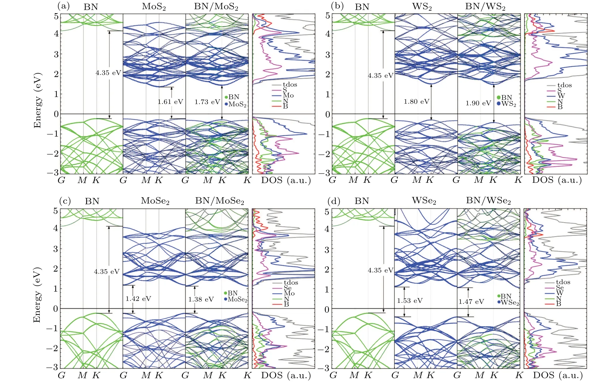
Figure 2 shows the band structures and atomic projected densities of states (PDOSs) of the heterostructures and their components. As can be seen from the band structures, the band gap of monolayer hBN,MoS2,WS2,MoSe2,and WSe2are calculated to be 4.35 eV, 1.61 eV, 1.80 eV, 1.42 eV, and 1.53 eV, respectively. As is well known, the PBE functional underestimates the band gap of hBN monolayer andMX2monolayer(Table 1). However, here in this work, we mainly focus on the trend of variation. Generally, the band gap and electronic states of the hBN/MX2heterostructure are significantly influenced by the interlayer contact. The electrons fromM(M=Mo or W)atoms contribute to the valence band maximum (VBM) and the conduction band minimum (CBM) in the PDOS(Figs.2(a)–2(d)),indicating that the band alignment of the heterostructure is of type-I. When they are stacked together,the band gap of the composed structures will be modified.For example,the band gap of the hBN/MoS2heterostructure is about 1.73 eV, slightly larger than that of the smaller band gap (herein MoS2) of component. However, the trend for the hBN/MoSe2is opposite, in which the 1.38 eV band gap value is 1.38 eV,smaller than minimum band gap of components(herein MoSe2).
It can be concluded that the electronic properties of the hBN/MX2(M=Mo, W, andX=S, Se) heterostructures are not simply a superposition of the two different materials even though the hBN andMX2layers are combined by van der Waals forces.
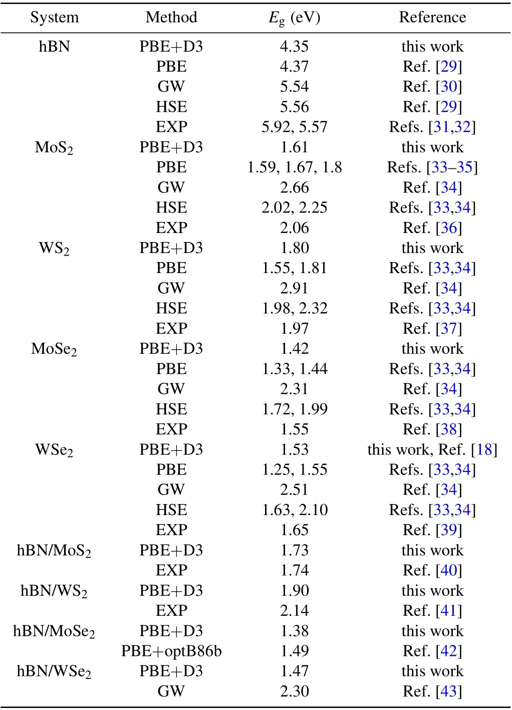
System Method Eg (eV) Reference hBN PBE+D3 4.35 this work PBE 4.37 Ref.[29]GW 5.54 Ref.[30]HSE 5.56 Ref.[29]EXP 5.92,5.57 Refs.[31,32]MoS2 PBE+D3 1.61 this work PBE 1.59,1.67,1.8 Refs.[33–35]GW 2.66 Ref.[34]HSE 2.02,2.25 Refs.[33,34]EXP 2.06 Ref.[36]WS2 PBE+D3 1.80 this work PBE 1.55,1.81 Refs.[33,34]GW 2.91 Ref.[34]HSE 1.98,2.32 Refs.[33,34]EXP 1.97 Ref.[37]MoSe2 PBE+D3 1.42 this work PBE 1.33,1.44 Refs.[33,34]GW 2.31 Ref.[34]HSE 1.72,1.99 Refs.[33,34]EXP 1.55 Ref.[38]WSe2 PBE+D3 1.53 this work,Ref.[18]PBE 1.25,1.55 Refs.[33,34]GW 2.51 Ref.[34]HSE 1.63,2.10 Refs.[33,34]EXP 1.65 Ref.[39]hBN/MoS2 PBE+D3 1.73 this work EXP 1.74 Ref.[40]hBN/WS2 PBE+D3 1.90 this work EXP 2.14 Ref.[41]hBN/MoSe2 PBE+D3 1.38 this work PBE+optB86b 1.49 Ref.[42]hBN/WSe2 PBE+D3 1.47 this work GW 2.30 Ref.[43]
3.2. Heterostructures with vacancies in hBN
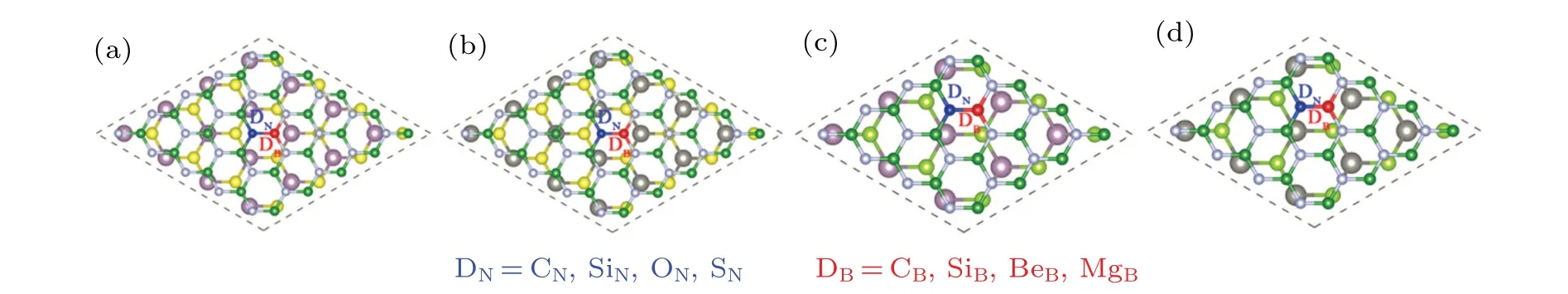
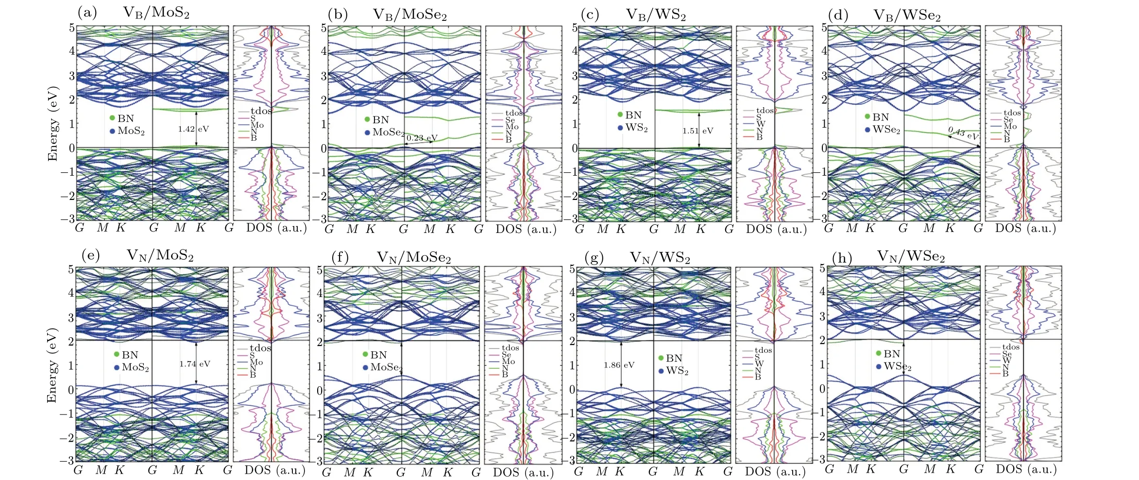
Vacancy defects usually exist in the experimental process of single-layer hBN prepared by electron beam irradiation and thermal annealing.[44,45]And vacancy defects have great effects on the excitation, migration, and recombination of photo-generated electron–hole pairs in semiconductor materials.Therefore,it is necessary to study the interface vacancy defects of heterostructures in detail. Here,the influences of B vacancy(VB)and N vacancy(VN),in hBN layer on the electronic structures of hBN/MX2(M=Mo, W, andX=S, Se)are investigated. Figure 3 shows the position of VBand VN,blue and red represent the removed nitrogen atoms and boron atoms,respectively.
Figure 4 shows the calculated energy band structures and atomic PDOSs of the heterostructures. The Fermi level of VB/MX2remains unchanged, while the Fermi level of VN/MX2shifts up to the conduction band. In addition, the energy band arrangement of VB/MX2is of type-II,while that of VN/MX2remains in type-I.Particularly,the degenerate energy level induced by boron vacancy is split in VB/MX2heterostructures. However, the system with vacancy defect still maintains semiconductor properties though their Fermi level crosses the energy band. It can be concluded that the interface vacancy defects can introduce the defect energy level into the band structure and change the energy band arrangement.
3.3. Heterostructures with substitutions in hBN
Doping is routinely employed to tune the electronic properties of semiconductors in many experiments.[46,47]The atoms of group(II,IV,VI)A are chosen as substitutional dopants to replace the B or N atoms of interface in hBN/MX2. These systems are described asD-hBN/MX2(D=BeB,MgB,CB,SiB,CN,SiN,ON,and SN). The top views of doped geometrical configurations are depicted in Fig.3. To achieve n-type doping,more than one electron will be inserted into the heterostructure for each of CB,ON,SiB,and SNdoping. On the other hand,CN,BeB,MgB,and SiNare examined for the effects of p-type doping in hBN/MX2,which a p-type doping hole is introduced into. Figure 5 shows the calculated energy band structures and atomic projected PDOSs of the atom-doped heterostructures. It can be seen that the energy band arrangement of CB/MX2is of type-I, while that of CN/MX2remains in type-II. The Fermi level of CB/MX2shifts up to the conduction band, while the Fermi level of CN/MX2keep unchanged. The carbon doped systems are greatly similar to the systems with vacancy defects. From this,it can be inferred that VN/VBhas n/p-type semiconductor properties. Figures S2 and S3(in supporting information)show other types of atomic substitution systems in detail.
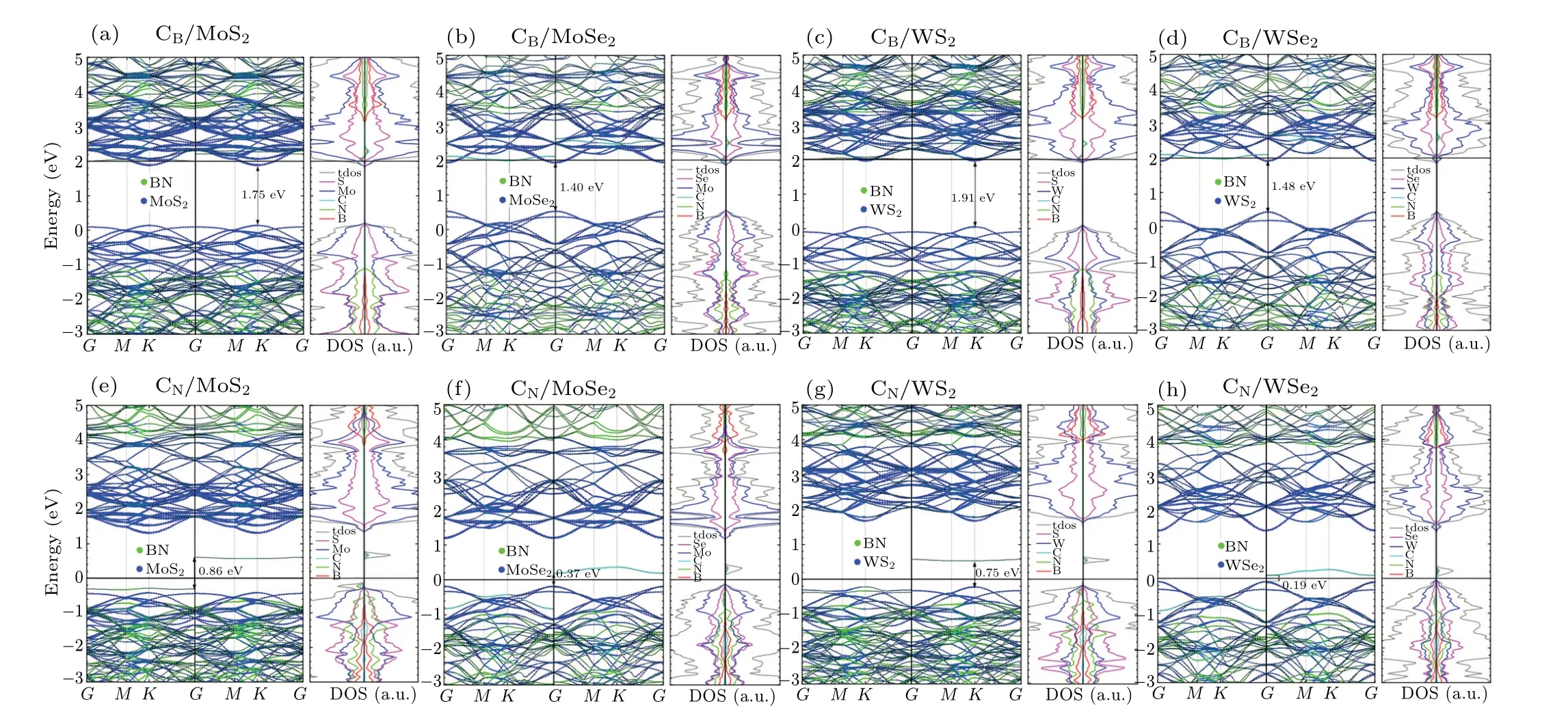
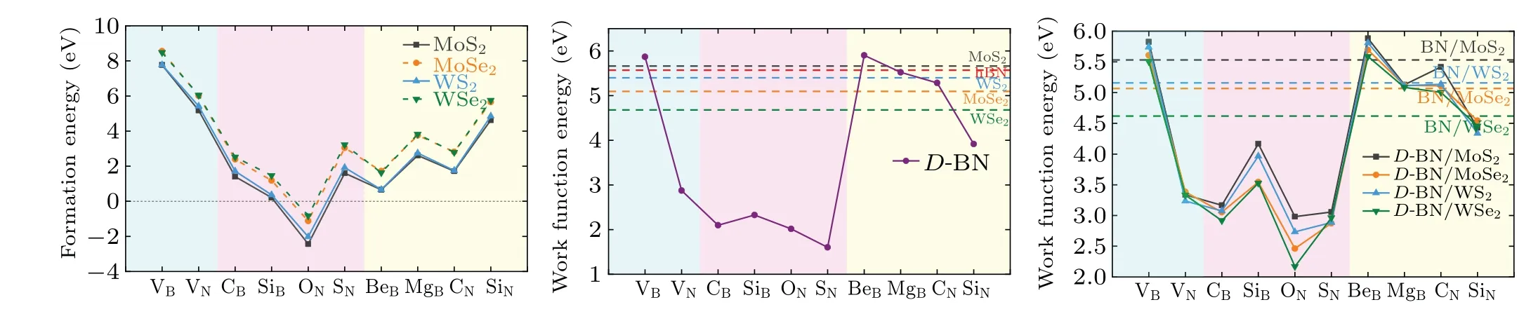
Figure 6(a) shows the variation of formation energy(Ef) for vacancy VB(VN)-hBN/MX2and for doping DB(VN)-hBN/MX2.In the experimental synthesis process,a positiveEfvalue means an endothermic reaction and a negativeEfvalue indicates an exothermic reaction. The lower theEfvalue,the more easily the reaction occurs. We find that among the four heterostructures based on MoS2,MoSe2,WS2,and WSe2,the hBN layer interface defect engineering is more likely to be realized on MoS2and WS2substrates. In addition, we can see that only ON/MX2reaction is exothermic, while other defect types of reactions are endothermic. This can be related to the differences in atomic radius and electronegativity between impurity atoms and B(N)atoms.
For different types of substituted atoms,electronic properties of the heterostructures will change differently. Simultaneously, the work function of the host material will be modified as impurity atoms are introduced, thereby affecting the ability to bind electrons. The work function can be defined as the difference between the vacuum and the Fermi level, and calculated from[48]
in whichEvacandEFare the vacuum level and Fermi level,respectively. Electrons will flow from the material with the low work function through the interface to the material with the high work function, making the two different materials positively and negatively charged,respectively,resulting in an internal electric field created at the interface.
Figure 6(b) shows the work functions ofD-hBN, with light blue,light magenta and light yellow regions representing the vacancy defects, n-type doping defects and p-type doping defects, respectively. Compared with intrinsic hBN, the work functions ofD-hBN (D=VN, CB, SiB, ON, SN, SiN,MgB, and CN) are reduced whileD-hBN (D=VBand BeB)become larger. Since the work functions ofD-hBN(D=VN,CB, SiB, ON, SN, and SiN) are lower than that of the idealMX2, the electrons will easily flow from theD-hBN toMX2through the interface. This contributes to speeding up the separation of photo-generated electron–hole combination due to a built-in field that points fromD-hBN (D= VN, CB, SiB,ON,SN,and SiN)to anMX2. Moreover,the direction of electric field points fromD-hBN(D=MgBor CN)toMX2in the heterostructures of MgB-hBN/MoS2,CN-hBN/MoS2,and CNhBN/WS2while the opposite orientation of electric field exists in the heterostructures of MgB-hBN/WS2,MgB-hBN/MoSe2,MgB-hBN/WSe2, CN-hBN/MoSe2, and CN-hBN/WSe2. We can preliminarily indicate that theMX2monolayer in the heterostructureD-hBN/MX2(D= VN, CB, SiB, ON, SN, and SiN) are acceptors of electrons and theD-hBN (D= VN,CB, SiB, ON, SN, and SiN) are donors of electrons. Conversely, theD-hBN (D=VBor BeB) andMX2act as acceptor and donor of electrons in the heterostructures (VB/MX2,BeB/MX2),respectively. Figure 6(c)shows the work function ofD-hBN/MX2. With respect to the ideal hBN/MX2, theDhBN/MX2reduces the work function to some extent,which is conducive to the electrons escaping from the hBN monolayer through the interface.
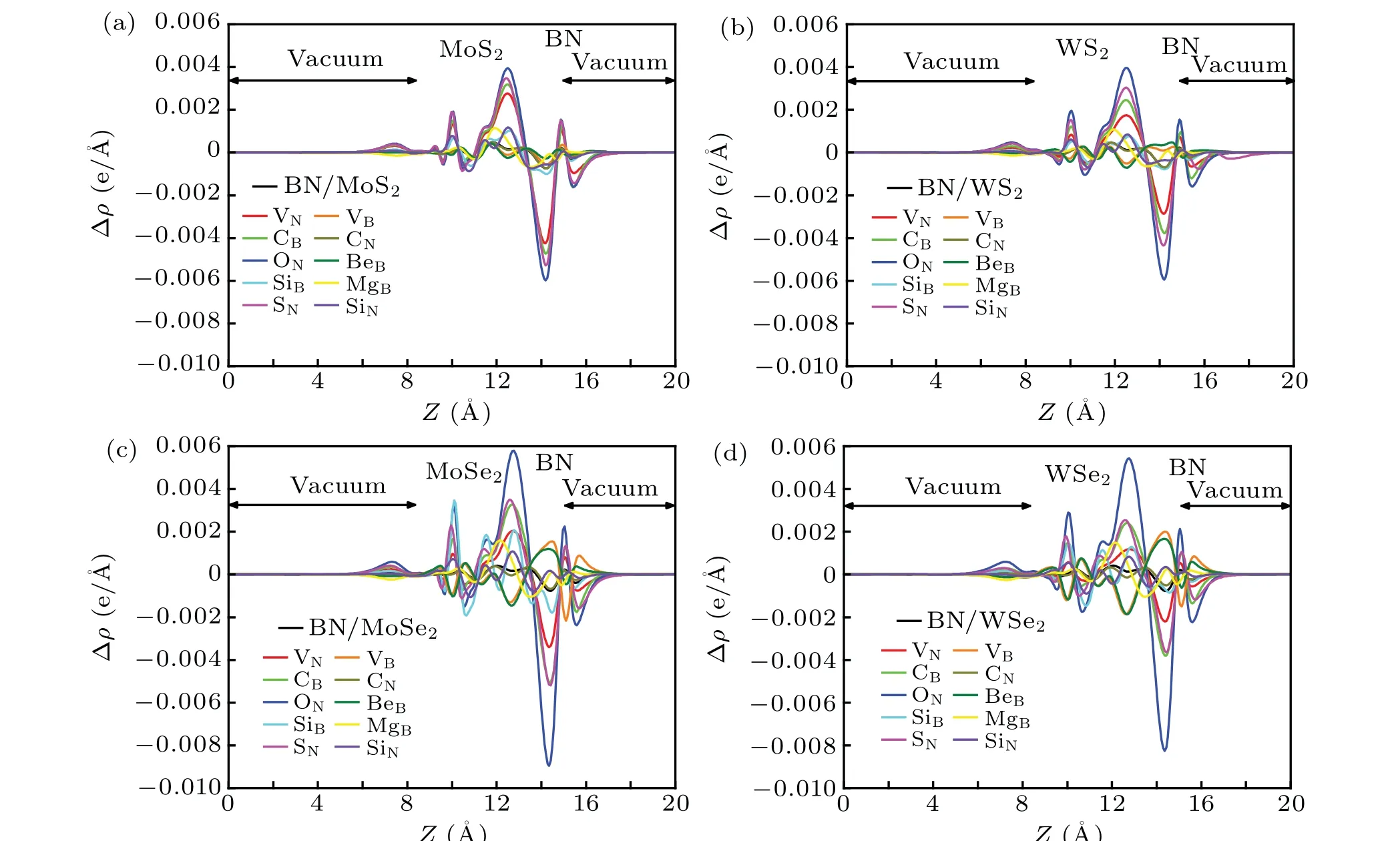
In order to understand the variations of the interface charge transfer and distribution with defect type and substrate materials in heterostructures,we plot the plane-averaged electron density differences along thezdirection of the hBN/MX2heterostructures as shown in Fig.7. Interestingly,we can find that in comparision with the ideal hBN/MX2, the transferred charge quantity of n-type dopedD-hBN/MX2(D=CB, ON,SiB,and SN)are significantly increased by 4 to 12 times. Especially in ON/MoSe2, the transfered charge quantity is the highest (1.5×10⁻²e), which is much higher than intrinsic hBN/MX2(1.4×10-3e),indicating that the interface interaction in ON/MoSe2is the strongest. In general, the larger the transferred charge quantity, the more conducive to the separation of photo-generated electron–hole pairs it is. It can be seen from Figs. 7(c) and 7(d) that the interface electrons ofD-hBN/MSe2(D=VBor BeB) are depleted on the upper of MoSe2or WSe2layer,while accumulate in hBN at the lower surface,thereby generating an electric field directing from theD-hBN (D=VBor BeB) to MSe2. Accordingly, the significant interfacial interaction makes the defect degeneracy level split in VB/MSe2electronic band structure. Furthermore, the induced shift in the electrostatic potential caused by the interface creation is depicted in Fig.S4,convincingly demonstrating the charge transfer direction.
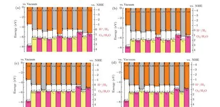
As is well known,in order to improve the photocatalytic activity, not only photo-generated electron–hole pairs are required to efficiently be generated, separated and transmitted,but also the occurrence of reverse reaction must be inhibited.These are closely related to the band gap value and band arrangement of heterogeneous composite photocatalysts. The band arrangement relative to the vacuum level can be achieved by calculating the band edge potentials of conduction band(CB)and valence band(VB)from the following formulae:[48]

The higher the CBM of photocatalyst(the more negative),the stronger the photoreduction capability is, while the lower the VBM(the more positive),the stronger the photooxidation capability is. As shown in Fig.8,the potential at the CB edge position ofD-hBN/MoS2(D=CB,ON,SN,and BeB)andDhBN/MoSe2(D=VN, CB, SiB, ON, SN, and BeB) are more negative than ideal reduction potential(0 V),while the potential at the VB edge position is more positive than ideal oxidation potential (1.23 V). This indicates thatD-hBN/MoS2(D=CB,ON,SN,and BeB)andD-hBN/MoSe2(D=VN,CB,SiB,ON,SN,and BeB)heterostructures can complete the redox reactions due to their suitable band edge potential.
Optical absorptivity,redox capability related to the position of conduction valence band, and effective separation of photo-generated carriers are the main reasons for the restriction on photocatalytic efficiency of traditional single semiconductor materials. But in the Z-type photocatalytic reaction system a two-photon excitation process is used to complete the oxidation reaction(2H2O+4h+→O2+4H+) and the reduction reaction(2H++2e-→H2)on different photocatalysts, respectively.[49–51]It can effectively inhibit the inverse reaction, showing significant advantages. We investigate the electronic properties of the BeB/MoS2, BeB/MoSe2,and VN/MoSe2vdW heterostructure,the results are shown in Figs. 9(a)–9(c), respectively. Although the energy band of defect-engineered hBN crosses the Fermi level, BeB/MoS2,BeB/MoSe2, and VN/MoSe2still maintain their semiconductor properties. Theoretically, there are three N atoms around each B atom in the hBN monolayer. When a single B atom is replaced by a Be atom,one N 2sp2and one N 2pzdangling bond will be left,resulting in an additional hole and making it a p-type semiconductor. In addition,removing one N atom to form VNwill induce three-B 2sp2and three-B 2pzelectronic dangling bond in the plane and make it an n-type semiconductor.
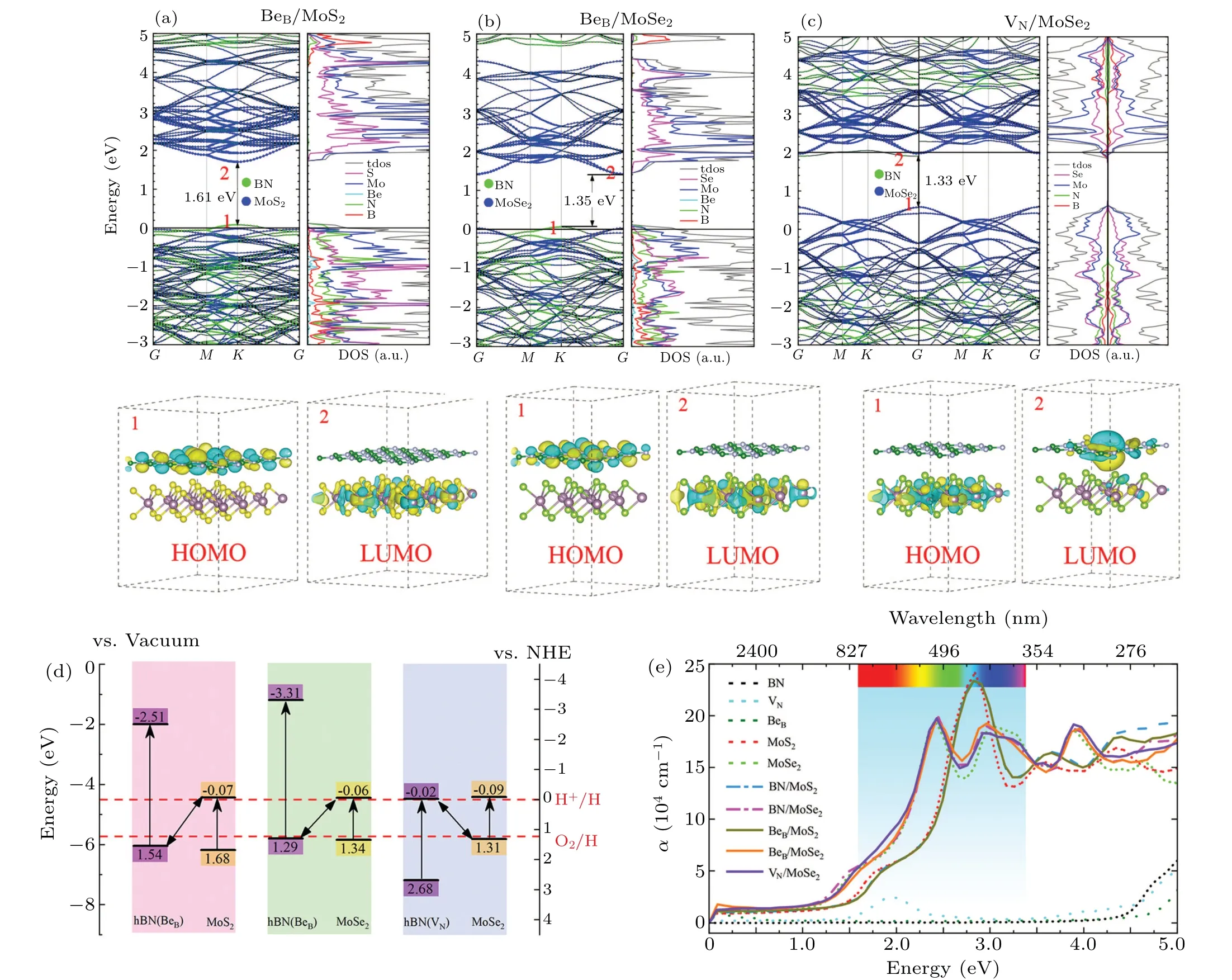
The highest occupied molecular orbital(LUMO)and the lowest unoccupied molecular orbital (HOMO) are marked with red numbers 1 and 2 in band structures as shown in Figs. 9(a)–9(c). In terms of real space, the HOMO of BeB/MoX2(X=S or Se)primarily derives from the hBN layer,with Pzorbital of N atom formingπbond, while LUMO is contributed by MoX2(X=S or Se)layer, forming aσbond.However, the situation of VN/MoSe2is opposite. These can be further demonstrated through the corresponding PDOS of BeB/MoS2,BeB/MoSe2,and VN/MoSe2,respectively. On the one hand,the appropriate band gap is 1.61 eV for BeB/MoS2,1.35 eV for BeB/MoSe2, and 1.33 eV for VN/MoSe2. On the other hand, the separation between the reduction process and oxidation process can effectively separate and transport photogenerated electron–hole pairs. Therefore,we can confirm that the BeB/MoS2, BeB/MoSe2, and VN/MoSe2heterostructure form a Z-type photocatalytic reaction system.
Figure 9(d) shows two Z-type photocatalytic reactions processes with opposite photo-generated carriers transferring directions. In BeB/MoS2or BeB/MoSe2,the photo-generated electrons of CB in MoX2(X= S or Se) with reduction reaction are prone to combining the photo-excited holes of VB in hBN(VN) with oxidation reaction. However, the direction of carriers transferring in VN/MoSe2is opposite to that in BeB/MoSe2. Compared with the traditional type-II heterostructure, the Z-type photocatalyst only needs to meet the requirement for its respective photoexcitation process and corresponding semi reactions, providing a tremendous space for the selection and design of photocatalytic materials. Generally, the optical absorption properties of photocatalytic semiconductor material are the macroscopic representation of its energy band structure. The calculated optical absorption coefficient of isolated monolayer, intrinsic and defect-engineered hBN/MX2bilayers are shown in Fig. 9(e). We can see that the defect-engineered hBN/MX2bilayers will effectively improve the absorption coefficient of visible light and make the red shift obviously appear at the absorption boundary.In short,our results indicate that the defect-engineered interfacial heterostructures can remarkly improve the photocatalytic properties of hBN/MX2(M=Mo,W,andX=S,Se)by tuning band arrangement,enhancing the interface charge transfer and light response, specifically the creation of Z-type heterostructures with high redox capability.
4. Conclusions
In this paper,the effects of interfacial defects on the electronic structure, charge transfer across the interface and photocatalytic properties of hBN/MX2(M=Mo, W, andX=S,Se) have been systematically investigated by the first principles calculation. After introducing vacancy and element doping, the n-type doped hBN/MX2(M= Mo, W, andX= S,Se) heterostructures maintain the I-type band arrangement,while the p-type doping changes the band arrangement from I-type to II-type. Comparing with the ideal hBN/MX2(M=Mo, W, andX= S, Se), the transferred charge quantity of n-type dopedD-hBN/MX2(D=CB, ON, SiB, and SN) are significantly increased by 4 to 12 times, in which the interface interaction of ON-hBN/MoSe2is the strongest. Two Ztype photocatalytic reaction processes with opposite photogenerated carriers transferring directions are achieved by defect engineering. With the help of two-photon excitation process, the reduction process and oxidation process are separated from each other. It includes efficiently separating and transmitting photo-generated electron–hole pairs, enhancing interfacial charge transfer and light response, and improving the stability of photocatalytic system. These theoretical results are expected to provide useful guidance for designing the novel high-efficiency photocatalyst based on hBN/TMDCs heterostructure.
Acknowledgements
Project supported by the National Key Research and Development Program of China(Grant No.2021YFB3802400),the National Natural Science Foundation of China (Grant Nos. 52161037, U20A20237, 51871065, and 51971068),the Scientific Research and Technology Development Program of Guangxi Zhuang Autonmous Region Province,China(Grant Nos. AD19110037, AA19182014, AD17195073, and AA17202030-1), the Guangxi Natural Science Foundation, China (Grant Nos. 2017JJB150085 and 2019GXNSFGA245005), the Innovation Project of GUET Graduate Education, China (Grant No. 2022YCXS197), the Guangxi Bagui Scholar Foundation, Guangxi Collaborative Innovation Centre of Structure and Property for New Energy and Materials, Guangxi Advanced Functional Materials Foundation and Application Talents Small Highlands, Chinesisch-Deutsche Kooperationsgruppe, China (Grant No. GZ1528),and the Guangxi Key Laboratory of Information Material,China(Grant No.201025-Z).
猜你喜歡
Chinese Physics B(2023年2期)2023-03-13 09:18:16
大江南北(2023年2期)2023-02-11 05:45:56
大江南北(2022年11期)2022-11-08 12:04:18
北京支部生活(2022年5期)2022-05-24 12:42:59
大江南北(2022年3期)2022-03-12 01:19:16
作文小學(xué)高年級(2021年10期)2021-11-08 09:13:40
作文小學(xué)中年級(2021年9期)2021-10-20 12:44:02
數(shù)學(xué)小靈通(1-2年級)(2020年11期)2020-12-28 00:41:20
海峽姐妹(2020年1期)2020-03-03 13:35:52
幸福家庭(2017年1期)2017-04-11 17:31:01

- Chinese Physics B的其它文章
- Switchable terahertz polarization converter based on VO2 metamaterial
- Data-driven parity-time-symmetric vector rogue wave solutions of multi-component nonlinear Schr¨odinger equation
- Neutron activation cross section data library
- Multi-phase field simulation of competitive grain growth for directional solidification
- A novel similarity measure for mining missing links in long-path networks
- Effects of electrical stress on the characteristics and defect behaviors in GaN-based near-ultraviolet light emitting diodes