
MOS-based model of four-transistor CMOS image sensor pixels for photoelectric simulation
2022-05-16 07:12:18BingZhang張冰CongzhenHu胡從振YouzeXin辛有澤YaoxinLi李垚鑫ZhuoqiGuo郭卓奇ZhongmingXue薛仲明LiDong董力ShanzheYu于善哲XiaofeiWang王曉飛ShuyuLei雷述宇andLiGeng耿莉
Chinese Physics B 2022年5期
Bing Zhang(張冰) Congzhen Hu(胡從振) Youze Xin(辛有澤) Yaoxin Li(李垚鑫)Zhuoqi Guo(郭卓奇) Zhongming Xue(薛仲明) Li Dong(董力) Shanzhe Yu(于善哲)Xiaofei Wang(王曉飛) Shuyu Lei(雷述宇) and Li Geng(耿莉)
1School of Microelectronics,Xi’an Jiaotong University,Xi’an 710049,China
2Key Laboratory of Micro-nano Electronics and System Integration of Xi’an City,Xi’an 710049,China
3National Key Laboratory of Science and Technology on Micro/Nano Fabrication,Peking University,Beijing 100871,China
4ABAX Sensing Inc.,Ningbo 315500,China
Keywords: four-transistor active pixel sensor(4T-APS),nonuniform doping,SPICE model,transfer gate,variable capacitance
1. Introduction
The excellent performance of CMOS image sensors(CISs) has led to the widespread use of pinned photodiode(PPD)based four-transistor active pixel sensors(4T-APSs)in various commercial and scientific areas. PPDs and transfer gates (TGs) are the two main components of 4T-APS. The heavily doped pinned layer isolates the charge storage region from the surface defects and traps that exist at the Si/SiO2interface, resulting in a low current leakage rate.[1–3]The nonuniform doping of TGs helps to stop the photogenerated electrons from being injected back to the photodiode,and thus eliminating the image lag.[4]Various key parameters such as the pinned voltage(Vpin), full well capacity(FWC),and PPD capacitance(CPPD)have been used to quantify the charge storage capacity and evaluate the features of the pixels.[5]As the core components of 4T-APS[i.e.,TG,PPD,and floating diffusion(FD)]directly affect the FWC,transfer efficiency, noise,conversion gain, and quantum efficiency of CIS, they have been widely discussed in the academia and industry.[6–9]
To determine the transfer characteristics of TGs,thermionic emission theory is applied in the qualitative explanation of image lag caused by the potential barrier.[10]Subthreshold current characteristics are used to analyze the charge transfer and image lag in TGs.[11]A second-order response system model based on the above theory has been established,[12–14]providing a more accurate physical model to explain the microscopic phenomena. As a result,several refined device designs have been developed.[15,16]For the PPD structure and its characterization,the relationship between the channel barrier height and FWC of the PPD during TG shutdown has been established.[12]The FWC qualitative analysis model of PPD uses the abstract pinned voltage model to fit the temperature and the concept of PPD capacitance.[10–17]The FWC model assumes a positive bias state and the equivalent theory of the depletion zone.[18,19]However,the test results are not in good agreement with the constant PPD capacitance model.[20]A variable capacitance model has been established based on mathematical analysis,[21]and a qualitative model based on the Fermi level equilibrium hypothesis has been reported.[10–22]Few studies,however,have attempted to identify how the TG functions together with the PPD influence the entire charge transfer process,and directly impact the charge transfer speed and the charge transfer efficiency. Additionally,there is no compact model that combines key parameters to reflect the entire operation process of PPD.[23]Furthermore, the above-mentioned models cannot be integrated into the SPICE framework. Thus,it is hard to effectively evaluate the compatibility between devices and system indicators.
Therefore,in this paper,we propose a matching approach with the MOS-based model to describe and simulate the working process of the 4T-APS pixels. The charge transfer process of the pixels is analyzed, and the role of nonuniform doping of TGs is investigated by using the resulting model. Finally,the effectiveness of the model is verified by the consistency between the simulation output and measurement results of a prototype PPD-based 4T-APS pixel.
2. MOS-based model in TGs
As shown in Fig. 1(a), there are two key design points in PPDs. (1) The photoelectric part: the width of the body depletion region and the pinned voltage are determined by the matching design of the epitaxial layer,pinned clamp layer,and the N-well implant concentration and depth. Thus, we can optimize the quantum efficiency (QE) of a specific spectral range and the PPD side potential during the photoelectric process. (2)The charge transfer part: to ensure the monotonicity of the potential distribution when the process of charge transfer from PPD to FD by the ON-state of TG, the size of the threshold voltage adjustment layer covering all PPDs and half parts of the TG channels. In TCAD simulation, the length of PPD and TG is 3 μm and 0.6 μm, respectively. In addition,the doping of TGs and threshold voltage adjustment layer is 4.5×1015cm-3and 2.2×1012cm-3, respectively. The potential distributions corresponding to the ON and OFF states of TG are respectively shown in Figs. 1(b) and 1(c). Therefore,TG+PPD cannot be regarded as an ordinary surface type four-terminal MOS device.

Fig.1. Typical TG and PPD structures. (a)doping diagram,(b)and(c)potential distributions corresponding to the ON and OFF states of TG,respectively.
The schematic of a 4T-APS built by a general SPICE model is shown in Fig. 2(a) (spectre circuit simulation environment). The PPD and TG are equivalent to an ideal current source in parallel with a constant capacitance and a symmetrical MOS transistor, respectively. The working principle is illustrated in Fig.2(b),where RESET MOS is used to reset the voltages of the FD and PPD capacitors, and the PPD capacitor is integrated by the current source (Iphoto). To change the FD potential,a TG MOS is used to redistribute the integrated charges in the FD and PPD capacitors. The simulation results of this 4T-APS circuit provide an input reference signal for a readout circuit,which may match the system timing but have no physical significance,as shown in Fig.2(b). The problems with this general SPICE model are as follows. (1) The photoelectric conversion characteristics of the PPD are expressed by a constant current source,which have no physical meaning.Because the equivalent of this method cannot represent the true current value that changes with the input light intensity and wavelength under the specific quantum efficiency of the device. (2)CPPDshould not be a constant capacitor,as a constant capacitance that can be reset to any voltage value cannot represent the clamping voltage characteristic of the PPD.The difference inVPPDafter switching off the TG twice in Fig.2(b)illustrates this problem. (3)A regular single threshold voltage of TG MOSFET model is not consistent with the characteristics of a nonuniform doping channel transfer gate. As shown in Fig. 2(b), theVFDdoes not change under differentVTGat 25 μs,and it is inconsistent with the physical process that different gate voltages will lead to different transfer efficiency.Thus, it is necessary to build a SPICE environment electrical model that reflects the whole physical process of 4T-APS pixel. Therefore,we propose a MOS-based combined model,including a photoelectric model and a transfer model to solve the above problems. The proposed approach is illustrated in Fig.3 and can be described as following.
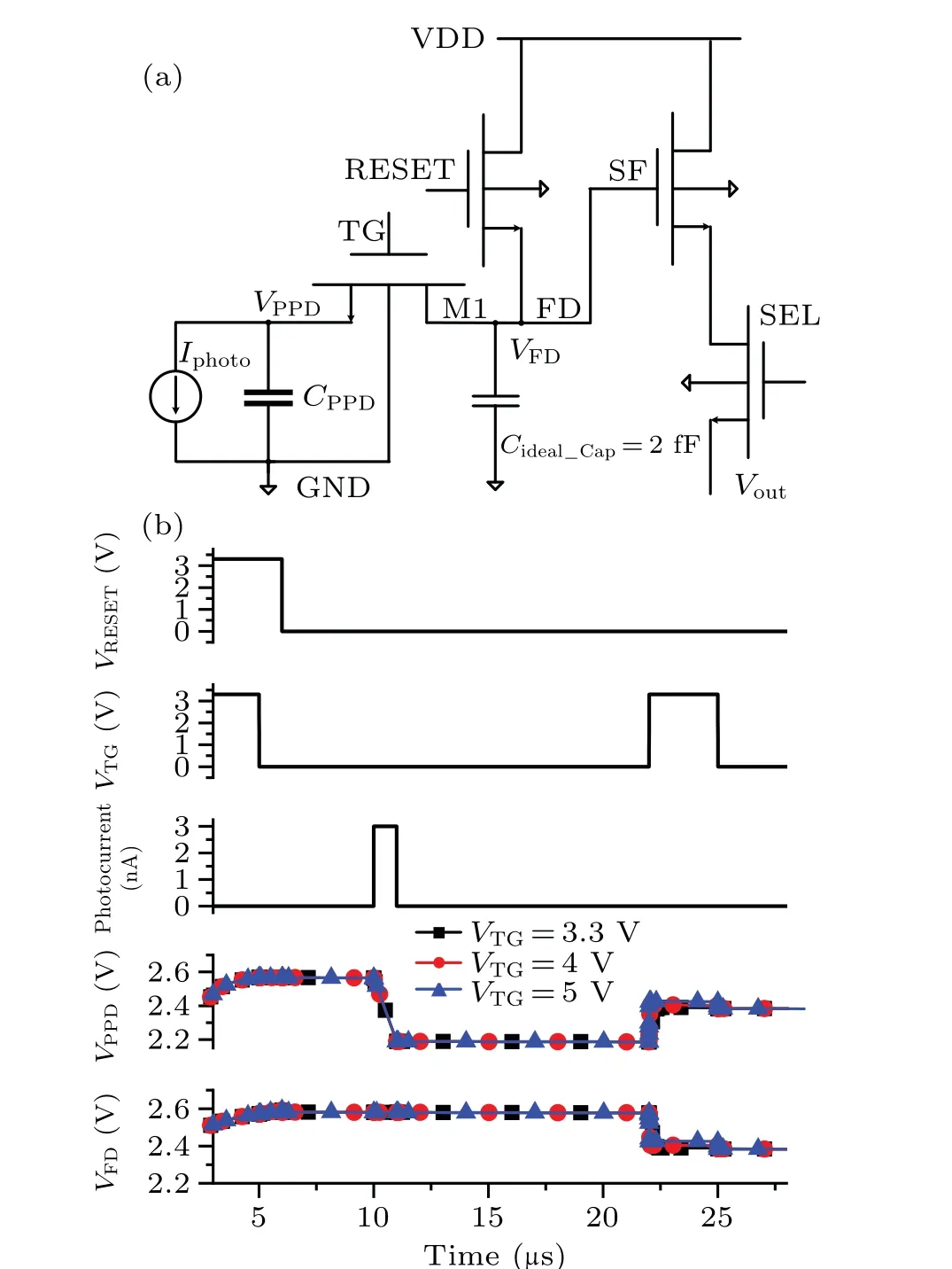
Fig.2. (a)Schematic of 4T pixel with a general SPICE model. (b)Simulation results of VPPD and VFD under different VTG are not consistent with the actual switching characteristics of TG.
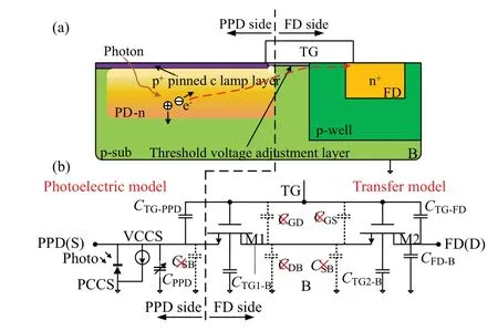
Fig. 3. (a) Structure of PPD and TG. (b) Corresponding schematic of MOS-based equivalent model.The dashed line capacitors represent that need to be removed compared to the regular MOS source and drain junction capacitance. The specific description is shown in Table 1.

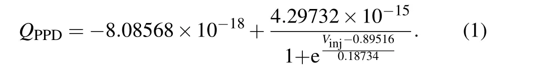
Fig.4. Charge of injection in PPD(QPPD)for varying injection voltage Vinj.
2.1. Photoeectric model
In this paper, a photoelectric model is setup to simulate the process of photoelectric conversion in the PPD,as shown on the PPD side of Fig. 3. The equivalence method is described in detail as follows.
Step 1 As shown in Fig.3,the PPD side of the TG is replaced by a pinned photodiode,where a variable PPD capacitance,CPPD,is substituted for the capacitance of the source end of the TG,CSB. To obtain the charge in the PPD(QPPD)versus voltage of PPD(VPPD)equation for capacitance model,a standard CMOS 4T-pixel with 3 μm pixel designed in 0.11 μm CIS process. TheseQ–Vmodels of PPD capacitances are also reported.[21–24]In the measurement setup, electrical injection of charges instead of optical integration is adopted to prevent measurement variations due to light. The drain voltage of reset transistor (VDD-RST) is externally controllable and the source of reset transistor is connected to the FD node.VDD-RST is the injected voltage (Vinj), which is varied to inject electrons via the floating diffuse node (FD) into photodiode well. The test curve ofQPPDand the corresponding injected voltage (Vinj) is shown in Fig. 4. The estimation ofVpinis done as[22]shown in Fig. 4. In region B, PPD is in a valid reset state,soVPPD=Vinj.The starting portion(region A)is dominated by the feed-forward effect[17](the read-out chain is not saturation). The tail portion(region C)is dominated by the pinning process and thermal emission. Only the middle portion can defineVPPDnormally. The quantitativeQPPD–Vinjrelationship that is accurately mathematical fitted according to the test data is as follows:
Step 2 Under this model, the input light is equivalent to a source terminal voltage at TG. The photodiode well is powered by light energy through a photoelectric conversion process. The photocurrent model is set up and the photon control current source(PCCS)originating from the photoelectric process is incorporated into the charge process of the PPD.In this work, in order to simplify the charging model of current source, only the photocurrent (Iph) is considered. Then, the photocurrent can be expressed as[25]

whereηis the quantum efficiency,λis the wavelength of light,andPoptrepresents the incident optical power. In this paper,ηof test device is 32%@905 nm through measurement. This innovative specific conversion process is as follows. Firstly,the relationship between the photocurrentIphof the PPD versus optical power and wavelength is obtained through Eq.(2).Secondly,the behavioral model of VCCS is constructed by the Verilog-A syntax. Thirdly, the charge generated by the photocurrentIphin the PPD,QPPD, is determined by the integral timetint. Fourthly,Eq.(1)is used to determineVinjandQPPDat the correspondingtintin PPD. Finally, the simplified photoelectric part of generation and collection have been established. This modeling method realizes the state that the internal voltage of the PPD changes with the generation of the photoelectric signal, and the voltage change will affect the PPD junction capacitance characteristics, so this feedback mechanism will affect the timely efficiency of the photoelectric collection. For integral optoelectronic devices, as the integrated charge of PPD increases,the PPD junction voltage decreases,and the photoelectric absorption efficiency tends to zero. The voltage value of the PPD side and the amount of transferable charge in the ON-state of the TG cannot be characterized by the traditional current source model.
2.2. Transfer model
The transfer model simulates the process of charge entering the FD from different doping regions of the TG. For the normal operation of a TG-based PPD structure, the inversion layer of the TG is created by the TG bias and the signal electrons are transferred into the FD region, as shown on the FD side of Fig.3.The model equivalence method can be described as follows.
Step 1 The PN junction model of the FD region needs some minor revisions to function as the drain terminal of the TG.We use the PN junction model of FD in a p-well provided by the CIS foundry. At the same time, the leakage current characteristics of the FD and PPD with respect to temperature can be obtained from the test results. These junction capacitances and leakage current parameters can be placed into the corresponding nodes.
Step 2 To model the nonuniform doping behavior of the TG under different threshold voltages. The purpose of this equivalence is to simulate the noise and charge injection effects of the TG switching process.Due to the nonuniform doping behavior of the TG,the channel electrons will monotonically transfer to the low-potential FD node during the TG turnoff process. We revise the Berkeley single channel IGFET model(BSIM;IGFET is an insulated-gate field-effect transistor)of a normal MOSFET to connect the modified MOSFET with differentVTHin series to act as the nonuniform TG, as shown in Fig. 3. Note that different values ofVTHare used to simulate the nonuniform doping of the TG channel in this model. This equivalence is based on theVTHmodel given by

whereφMSis the work function difference between the gate and the substrate,φF=(kT/q)×ln(Nsub/ni),Nsubis the doping concentration of the substrate,Coxis the gate oxide capacitance per unit area, andεsiis the dielectric constant of silicon. As shown in Fig. 3, the substrate under the TG channel is doped under different conditions, so it is reasonable to use a low threshold voltageVTH-Lto characterize light p doping and a high threshold voltageVTH-Hto characterize heavy p doping in the TG channel. Therefore,W/Lfor each MOSFET is determined under two differentVTHconditions according to the actual injection size of the TG channel.
Step 3 Adjust the capacitance and current density parameters in the BSIM of the series MOSFETs described in step 2. Parameters such asjunction capacitance of source or drain end per unit area (CJ), sidewall junction capacitance per unit periphery (CJSW), gate drain overlap capacitance per unit width (CGDO), gate source overlap capacitance per unit width(CGSO),bottom source junction reverse saturation current density(JSS), isolation edge sidewall source junction reverse saturation current density (JSWS), gate edge source junction reverse saturation current density (JSWGS), bottom drain junction reverse saturation current density (JSD), isolation edge sidewall drain junction reverse saturation current density (JSWD), and gate edge drain junction reverse saturation current density (JSWGD) are considered. Because the actual nonuniform doping TG is a source–drain asymmetrical two-terminal device, part of the node devices will be deleted in the dual MOS structure model, as shown in Fig. 3(b).The BSIM capacitances and current density parameters are presented in Table 1, whereLDis the drain/source diffusion length,Weffis the effective width,Lthe channel length,MJis the exponent in the CJ formula,VBSis the voltage between body and source end,VBDis the voltage between body and drain end,CFis the full well capacitance,CGSis the capacitance between gate and source end,CGBis the capacitance between gate and bulk,CBDis the capacitance between bulk and drain end, andCSBis the capacitance between bulk and source end.
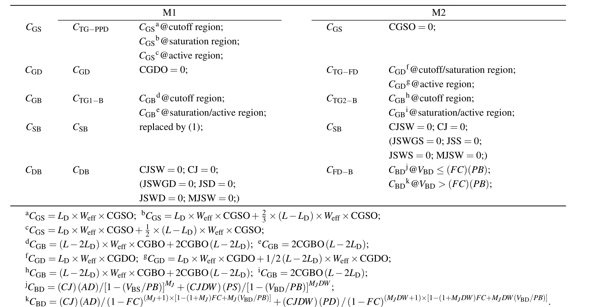
Table 1. BSIM parameters of MOS-based model.
3. MOS-based model in 4T pixels
Combining the above two models gives the whole MOSbased model. The photoelectron generation and charge transport behaviors of signal electrons from PPD to FD and the role of the TG in the charge transfer process are investigated.The leakage current model is not considered in this simulation. A schematic of the 4T pixel with the proposed MOSbased model is shown in Fig.5,where the threshold voltages of M1 and M2 are set to 0.8 V and 0.4 V, respectively, as an example. The quantum efficiency(η=30%)and wavelength of light(λ=905 nm)are chosen in this work. The simulation timing include reset, integration, correlated double sampling(CDS)reset and readout phase.

Fig.5. Schematic of 4T pixel with MOS-based model.
As shown in Fig.6,we can observe that the TG switches off during the reset phase,and theVPPDdecreases from 2.8 V to 1.45 V under illumination. Due to the charge injection effect of the TG,some electrons are injected into theCPPD,that is, theVPPDcan quickly decreases to theVpinlike region C in Fig. 4. The value ofVFDremains almost constant because it is still connected to the VDD terminal through the RESET transistor,the clock feedthrough effect introduced by the RESET switching cannot affect the voltage of the FD node before the TG is turned on,so the injected electrons are also pumped away by this process. However,VFDsuffers from the charge injection and the kTC noise of the RESET transistor when it is off.
Then,the light is on after reset phase,and the photogenerated electrons are integrated in the PPD capacitance by a 905 nm light with a power density of 0.05 W/cm2for 7 μs,which leads to theVPPDnonlinear decrease from 1.45 V to 0.72 V. Therefore, it is proved that the variable capacitance can accurately simulate the current and voltage characteristics of the PPD in the photoelectric simulation than the conventional current source.
The TG then switches on and the signal electrons start to flow from PPD to FD after CDS reset phase, causing a decrease inVFDand a increase inVPPD. When the TG switches off again, the coupling effect from the TG causesVFDto decrease again. This process implies that when the TG switches on,some of the photo generated electrons are absorbed by the inversion layer of the TG,and other electrons transfer to FD.The inversion electrons will be kicked back to both FD and PPD when the TG switches off. The charge injection from the TG causes some of the photo generated electrons to flow back to PPD,and the potential barrier/pocket under along the electron path is the main reason that affects the electron lag.After using the MOS-based model to be equivalent,these potential effects are replaced by the channel on-resistance and the switching charge sharing effect. Therefore,the photoelectron generation and charge transport behaviors ofVPPDandVFDcan be expressed correctly by using the above two models to give the whole MOS-based model.
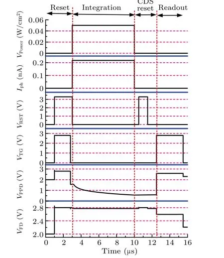
Fig.6. Simulation results of 4T pixel with MOS-based model.
4. Model validation
4.1. Modeling the charge injection effect by different threshold voltages
To investigate how nonuniform doping could suppress the charge injection effect of the TG, the MOS-based model was executed with three different threshold voltage combinations according to the conditions in Fig. 5. The simulation results are summarized in Table 2. The charge injection from TG to PPD in case A (VTH-M1=0.8 V andVTH-M2=0.4 V) is only 0.0016%, much lower than the 6.49% in case B(VTH-M1=0.4 V andVTH-M2=0.4 V)and 9.12%in case C(VTH-M1=0.4 V andVTH-M2=0.8 V).Case B characterizes the switching characteristics and charge injection effects of a conventional symmetric MOSFET.The simulation results in cases B and C do not match the switching characteristics of TGs. These results confirm the effectiveness of nonuniform TG doping with different threshold voltages MOS-based model in suppressing the charge injection effect and improving the device performance of charge transfer efficiency. This paper focuses on the use of MOS-based models to characterize the integration and transfer characteristics of optoelectronic devices,so discussion on device optimization is ignored.
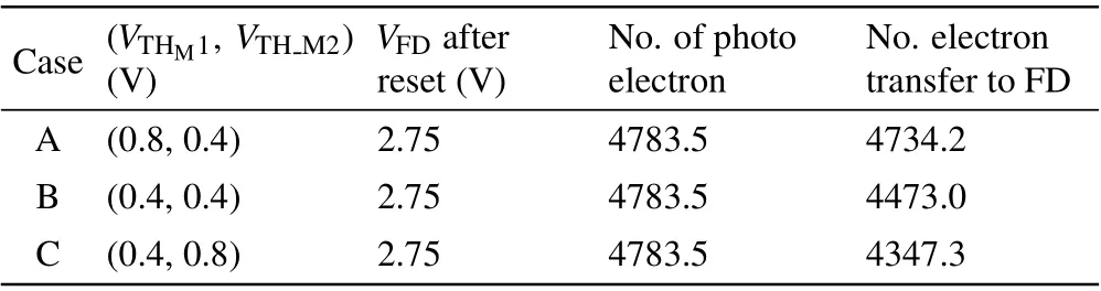
Table 2. Charge number under different VTH and reset conditions(VTG=2.8 V,VRST=3.3 V).
4.2. Modeling charge transfer efficiency by TG voltage
We further studied how the gate voltage of the TG influences charge transfer efficiency (CTE) of the pixel both in MOS-based model and TCAD simulations. The condition of case A (in Table 2) and timing process like Fig. 6 are used in MOS-based model simulation. All the simulations are performed at a temperature of 300 K. By comparing the results from these two channel length conditions,the working mechanism of nonuniform TG doping can be determined.It is important to note that only the trend of relationship betweenVTGand CTE is considered in this work. As shown in Fig.8,the model potential can not match the actual potential perfectly. The actual potential from PPD to FD change gradually,which is not as same as the stepped potential distribution in MOS-based model. And some second-order effects like both the thermal emission and drain induced barrier lowering(DIBL)can lead to differences in the model and TCAD simulation. As shown in Fig. 7, when theVTGdrops from 2.8 V to 1.5 V, the CET decreases approximately linearly from about 100% to 72%.However,the CTE drops from 53%to 21%whenVTGchanges to 1.5 V. This is mainly due to the M1 transistor enters the sub-threshold region, which leads to the sharp deterioration of CTE. Similar trend can be observed in TCAD simulation,and the knee point of CTE changes sharply atVTG= 2 V.The thermal emission effect will help the electrons overcome the barrier to transfer to FD at lower the barrier. Although the specific value and knee point are not well matched,this model can reflect the trend of changing.

Fig.7. The trend of charge transfer efficiency versus VTG.
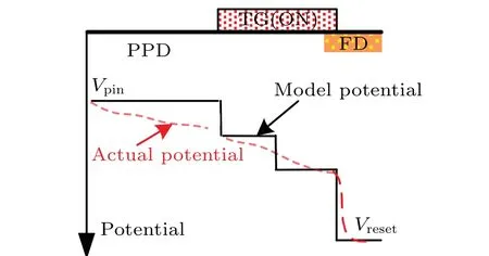
Fig.8.Equivalent potential distribution condition of MOS-based model and TCAD simulation.
4.3. Modeling the transient variation of VPPD by different light power
TheVPPDis a physical parameter inside the device,which cannot be directly characterized by real-time testing, therefore, it is necessary to do the transient photoelectric simulation by TCAD to directly characterize the variation ofVPPD,which can also well verify the correctness of model. The TCAD simulations adopt the same timing as Fig. 6 to compare with MOS-based model results. The voltage variation ofVPPDin integration time interval(2.8 μs to 12.5 μs)is shown in Fig. 9. Three typical cases of light power were selected to compare the fitting between TCAD and model simulation data. The best fitting has been obtained with small light power(VPower=0.005 W/cm2)as shown in red line and circle makers in Fig. 9. In the photocurrent model,[21]the total current(Itotal)contribution at PPD node is given as


Fig.9. The VPPD as function of integration time for three different light power. Circle markers represent TCAD simulation data and solid lines represent model simulation data.
4.4. Modeling the variation of VFD by test verification
As shown in Fig. 10, the effectiveness of the MOSbased model is verified by the testbench. The light source is an integrating sphere with a 905 nm laser diode, and the measurement-control system is based on Xilinx’s Kintex-7.The test circuitry consists of a standard 4T-APS with a PPD with 3 μm pixel, and theW/Lof the TG is 1.0 μm/0.6 μm.VDD RST is fxied to 2.8 V,which is used to reset the FD and PPD regions to a higher potential level. The global analog buffer circuit is used to read out the signals under the test environment temperature of 300 K.The test timing is as same as Fig.6 and the results of the FD voltage are shown in Fig.11.Without any light after reset, the FD voltage rises to a high level. Both in the model and TCAD, the FD node is reset to 2.8 V, and theVFDof test pixel is 1.82 V due to the source follower (SF). The threshold voltage of SF is adjusted to be 0.4 V in this work. The FD voltage decreases when the reset signal is off because of the charge injection effect, however, lagerVFDvariation was observed in measurement. This mainly caused by the parasitic coupling of wire. FD node is very sensitive as read-out node in 4T structure,and moreover,the capacitance of FD is only 2 fF in this work. Therefore,the clock feed through effect of parasitic capacitance will causeVFDto decrease greatly after reset in the measurement data curve. In the meantime,the same phenomenon and trend were observed during CDS reset period. When PPD is integrated by a 905 nm laser diode for 7 μs, there is a slight drop ofVFDin measurement and TCAD curve due to the subthreshold leakage and direct photogenic effect of FD node. When the TG is on again after integration,one part of electrons will transfer directly from PPD to FD,resulting in the drop ofVFD,and the other part of electrons will be stored under the TG gate as inversion layer electrons. This part of electrons will be released again to FD node when TG is turned off. The two parts of the signal electrons constitute the signal change ofVFD. As shown in Fig.9,the variation ofVFDin measurement is smaller than TCAD and the model,it is understandable because the light power intensity can not be calibrated and match with the model well.All these behaviors trend can be obtained by using the circuit simulation based on the proposed model,TCAD and measurement, demonstrating the effectiveness of our approach.

Fig.10. Test platform and test structure of test chip diagram.

Fig.11. Test curves of VFD as function of integration time. TCAD and the proposed model simulations are compared together.
During the process simulation, the Monte Carlo implantation model is used. The doping-dependent mobility models,Shockley–Read–Hall model,Auger recombination model,Fermi–Dirac statistics optical generation model and compact SPICE model are activated in Sdevice simulation. The mesh number (about 100000) and minimum mesh size (2 nm) are optimized for simulations. The hybrid simulation of 4T-APS in TCAD usually takes about one day in this work. However, the MOS-based model can characteristics the function of nonuniform doping of TGs in suppressing charge injection back to PPDs like TCAD simulation with a few minutes.So, compared with the hybrid simulation in TCAD and the
Verilog-A simulation in SPICE,this model has higher simulation efficiency and accuracy,respectively.
5. Conclusions
A combined MOS-based model has been developed by considering the variable capacitance characteristics of PPD and the nonuniform doping in the TG channel. The SPICE simulation conclusion of this model was verified by TCAD simulations and test results. The charge transfer process of photogenerated electrons from PPD to FD was analyzed and the function of nonuniform TG doping in suppressing charge injection back to PPD was studied. The proposed model characterizes current and capacitance characteristics of the TG source terminal correctly. As a result,SPICE simulations can be successfully performed by combining all the physical characteristics of the PPD and TG, giving an effective evaluation mechanism for hybrid optoelectronic processes. In addition,with the help of the model, pixel design can be rapidly iterated to match the system design. This model introduces the possibility of system-level simulation in the design of lowillumination and low-noise-response CIS and high-speed modulation of the time of flight (TOF) pixels. Future work will consider the quantitative analysis of the overlapping potential barrier, total current, gate voltage, and threshold voltage for TGs more detailed.
Acknowledgements
Project supported by the National Natural Science Foundation of China (Grant No. 61874085) and the Postdoctoral Research Funding Project of Shaanxi Province, China(Grant No.2018BSHEDZZ41).

- Chinese Physics B的其它文章
- Erratum to“Boundary layer flow and heat transfer of a Casson fluid past a symmetric porous wedge with surface heat flux”
- Erratum to“Accurate GW0 band gaps and their phonon-induced renormalization in solids”
- A novel method for identifying influential nodes in complex networks based on gravity model
- Voter model on adaptive networks
- A novel car-following model by sharing cooperative information transmission delayed effect under V2X environment and its additional energy consumption
- GeSn(0.524 eV)single-junction thermophotovoltaic cells based on the device transport model