
First-principles calculations of the hole-induced depassivation of SiO2/Si interface defects
2022-05-16 07:11:14ZhuoChengHong洪卓呈PeiYao姚佩YangLiu劉楊andXuZuo左旭
Chinese Physics B 2022年5期
Zhuo-Cheng Hong(洪卓呈) Pei Yao(姚佩) Yang Liu(劉楊) and Xu Zuo(左旭)
1College of Electronic Information and Optical Engineering,Nankai University,Tianjin 300350,China
2Microsystem and Terahertz Research Center,China Academy of Engineering Physics,Chengdu 610200,China
3Institute of Electronic Engineering,China Academy of Engineering Physics,Mianyang 621999,China
4Municipal Key Laboratory of Photo-electronic Thin Film Devices and Technology,Nankai University,Tianjin 300350,China
5Engineering Research Center of Thin Film Optoelectronics Technology,Ministry of Education,Nankai University,Tianjin 300350,China
Keywords: a-SiO2/Si interface,hole,depassivation,first-principles calculation
1. Introduction
The amorphous a-SiO2/Si interface plays an important role in semiconductor devices and directly affects device performance. The Si dangling bonds at the interface are usually referred to as Pbdefects(also known as interface traps),which is the intrinsic defect type in an a-SiO2/Si interface.[1—3]In the fabrication of semiconductor devices, H atoms are commonly used to passivate electrically active Pbdefects to improve the quality of the SiO2/Si interface.[4,5]The saturated Si atom dangling bond at the interface can not only depassivate with hydrogen[6—8]but can also interact with the carrier,[9—16]breaking the Si—H bond and activating the interface defects.The Si—H bond-breaking mechanism at the interface is an important step in the process of Si dangling bond formation.The experimental (theoretical) values for the forward and reverse reaction barriers are 2.83(2.57)eV and 1.51(1.31)eV,respectively.[17,18]
In Ref. [9] Guerinet al.focused on the different bond states under carrier-induced excitation and proposed a theoretical mechanism considering various pathways to excite a Si—H bond by carriers. It was pointed out that the Si—H bond breaking process can be attributed to the multiple vibrational excitation mechanism,in which many carrier—bond interaction events are required to provide sufficient energy for bond dissociation.
In a recent study, the mechanism of hot-carrier degradation was simulated by Jechet al.usingab initiodensity functional theory(DFT)calculations.The carriers interact with the Si—H bond at the interface, which is known as the resonance mechanism. In that study the physical process of electron/Si—H bond interaction was discussed in detail.[10]
Under ionizing radiation, electron—hole pairs are created in the oxide semiconductor.[19,20]Those carriers lead to charge buildup, which can degrade the performance of the device.[21—27]Winokur stated that holes can induce interface states. At the first stage of the appearance of interface states,about 5 eV of energy is released by capture of the radiationgenerated holes near the SiO2/Si interface, resulting in the relatively weak Si—H or Si—OH bonds breaking at the interface. In the second stage,the interface state is generated when enough energy is released to break the Si—H bonds. Dissociation of the metastable configuration and the diffusion of weakly bound ions from the ‘broken bond’ site leads to interface states.[11]
In 1995, DiMaria proposed that the holes in the oxide might degenerate the SiO2/Si interface, thus producing interface states. It was reported that the formation of interface states is caused by holes in a two-step process.[11,27—29]First,holes keep approaching the interface and are captured by the interface, but no interface states appear at this moment. In the second step,electrons are recombined with trapped holes,creating interface traps. However,in subsequent experiments,hole injection without electrons could still produce interface traps.[30]
Moreover, ionizing radiation can lead to the generation of holes in SiO2, as has been confirmed in many studies.The holes induced by ionizing radiation react with the saturated SiO2/Si interface defects,leading to interface traps.[30,31]However,there is no consensus on the essential reaction mechanism of the depassivation of the interface defects by holes. In this work we investigate the depassivation of the SiO2/Si interface defects by holes (HPb+h→P+b+H). The reaction curves,the barriers associated with the transition state and the distances between active atoms(Si,O,and H)in the reaction are obtained via the climbing image nudged elastic band(CINEB)method to simulation the depassivation reaction. In addition,the valence electron numbers on active atoms are analyzed using the Bader charge method.
2. Methods
The a-SiO2/Si(111)interface is an ideal model for scientific research,while the a-SiO2/Si(100)interface is commonly used in actual devices. In this work,the interface defect models are derived from Refs.[32,33]. The supercell dimensions of the defect-free a-SiO2/Si(100) (a-SiO2/Si(111)) interface,which contains 329 (353) atoms, are 15.47 °A×15.47 °A×47.86 °A(13.30 °A×15.36 °A×49.39 °A)(Fig.1). To make this work more persuasive and generalized, four Pb-type defects are studied: Pbdefects in the a-SiO2/Si(111)interface[32]and Pb1-bridges, Pb1-asymmetrically oxidized dimers (Pb1-AOD)and Pbdefects in the a-SiO2/Si(100)interface.[33]
Due to the large number of atoms in the model, firstprinciples calculations based on DFT implemented in Viennaab initiosimulation package (VASP) are applied to relax the structures of the interface.[34—37]In order to save computing resources, the relaxation process is carried out in two steps,in which the cut-off energy is set to 350 eV and 520 eV, respectively. In addition,an accuracy of 10-5eV and 0.05 eV/°A is adopted for the electronic loop and ionic loop,respectively.The generalized gradient approximation is used to optimize the structure until the residual stress on each atom is less than 0.05 eV/°A.Due to the relatively large unit cell size,sampling and integration are only performed at theΓpoint of the Brillouin zone.
The CI-NEB method is implemented to search the saddle point and the minimum energy path of a reaction.[38]According to the reaction equation (HPb+h→Pb+H+), the initial model of the NEB simulation is built after structural optimization with the addition of a hole by removing an electron from the neutral system. The final model is obtained by constructing a proton bonded to an O atom and optimizing the atomic structure by removing an electron.
In order to calculate the number of active valence electrons on the atoms and figure out the charge transfers in the reactions,Bader charge analysis[39—41]is employed. Although the Bader charge method is more accurate than other analytical methods,the number of valence electrons obtained by the Bader charge method may not be an integer. Therefore,when analyzing the change in the number of valence electrons in the transition state, the structure of the transition state, electron transfer and system energy should be taken into consideration.

Fig.1. The defect-free a-SiO2/Si interface model: (a)a-SiO2/Si(100)interface model;(b)a-SiO2/Si(111)interface.
3. Results and discussion
3.1. Pb1 defect of the SiO2/Si(100)interface
3.1.1. Pb1-bridge defect
The construction of the initial and final structures simulated by CI-NEB is described in Section 2. In the initial state of the reaction (Fig. 2(a)), the length of the Si—H bond is 1.46 °A(ideally,the Si—H bond is~1.5 °A),and the distance between the H atom and the O atom is 3.81 °A.Moreover,the total number of valence electrons on the Si,O,and H atoms is 12.93(Table 1).From the 00 state to the 01 state(Fig.3(a)),as the reaction moves forward,the length of the Si—H bond keeps increasing and the H atom gradually approaches the O atom.

Fig. 2. Initial and final states of the hole-induced depassivation reaction of a Pb1-bridge defect in the SiO2/Si(100) interface: (a) initial state; (b) final state.
In the 02 state(Fig.3(b)),the number of valence electrons on the Si and H atoms becomes 1.78 and 2.00, respectively,while that on the O atom remains unchanged. Compared with the previous state, about 1.17 holes are captured by the saturated defect center(the Si—H bond). This is the first step in the reaction, where the Pb1-bridge defect traps a hole with a barrier of 0.50 eV.At this time,the Si—H bond is stretched but not yet broken,resulting in an unstable system. In the subsequent step, the system reaches the transition state as a result of the Pb1defect capturing one more hole.

Table 1. Number of valence electrons on the active atoms,the length of the Si—H and H—O bonds and system energy in hole-induced depassivation of Pb1-bridge defects. 00, 03, 05 mark the initial, transition and final states,respectively.

Fig. 3. Intermediate states of the hole-induced depassivation reaction of a Pb1-bridge defect in the SiO2/Si(100)interface: (a)01 state;(b)02 state;(c)03 state;(d)04 state.
When the reaction proceeds to the transition state 03(Fig. 3(c)), the Si—H bond breaks and the H atom gradually moves away from the Pb1defect. When the distance between the H atom and the O atom is 1.23 °A, a H—O bond begins to form but is not yet complete.Compared with the previous state(02 state), the Si dangling bond captures an extra 0.8 holes from nearby atoms. In addition,charge transfer occurs inside the defect center, so that the number of valence electrons on the Si atom slightly increases to 2.92,and that on the H atom decreases to 0.19. This indicates that the transition state (03 state)can be regarded as the second step in the depassivation of the Pb1-bridge defect by holes. In Fig.4,the energy of the system at this state rises to 2.44 eV(Fig.4),reaching a maximum.
As the reaction proceeds, in the third step of the holeinduced depassivation reaction the Pb1-bridge defect center captures about 0.9 electrons in the 04 state(Fig.3(d)),resulting in a Si dangling bond with 3.79 valence electrons. In the final stage of the reaction (Fig. 2(b)), the length of the H—O bond is 0.99 °A,which is coincident with the ideal value of the proton—O bond length,and thus the Pb1-bridge defect is depassivated. At this point,the total number of valence electrons on the Si,H and O atoms is 11.93,which is about 1 electron less than in the initial state,equivalent to consuming a hole in the whole reaction. The energy of the final state is 1.97 eV,which is lower than the saddle point by 0.47 eV.

Fig.4. Reaction curve of hole-induced depassivation of a Pb1-bridge defect in the SiO2/Si(100)interface(green curve). The black square,red circle and blue square mark the number of valence electrons in the active Si,O,and H atoms,respectively.
3.1.2. Pb1-AOD defect
The CI-NEB calculation is employed to search for the minimum energy path of the hole-induced depassivation reaction (Fig. 5). In the initial state (Fig. 5(a)), Table 2 shows that the length of the Si—H bond is 1.48 °A, and the distance between the H and O atoms is 2.99 °A. The total number of valence electrons on the Si, O, and H atoms is 12.71. In the 01 state (Fig. 6(a)), the length of the Si—H bond is increased by 4.72%, while the distance between the H and O atoms is reduced by 24.08%compared with that in the 00 state.

Fig.5. Initial and final states of the hole-induced depassivation reaction of a Pb1-AOD defect in the SiO2/Si(100)interface: (a)initial state;(b)final state.
When the reaction proceeds to the transition state 02(Fig.6(b)),the Pb1-AOD defect captures about 2.2 holes with an energy of 2.19 eV. In this state, the Si—H bond is broken,leaving a Si dangling bond with two positive charges. The number of valence electrons on the Si atom and the H atom is 2.02 and 0, respectively, while that on the O atom remains constant.
As the reaction moves on, in the 03 state(Fig.6(c)), the Si dangling bond captures about 1.6 electrons. This is the last step in the hole-induced depassivation reaction, where a Si dangling bond with a valence electron number of 3.87 appears. In this state,the Si—H distance stretches to 3.25 °A,and the length of the H—O bond is reduced to 0.99 °A. Moreover,the reduction in energy is small,only about 0.18 eV less than that in the 02 state.

Table 2. Number of valence electrons on the active atoms,the length of the Si—H and H—O bonds and system energy in hole-induced depassivation of a Pb1-AOD defect. 00, 02, 04 mark the initial, transition and final states,respectively.

Fig. 6. Intermediate states of the hole-induced depassivation reaction of a Pb1-AOD defect in the SiO2/Si(100)interface: (a)01 state; (b)02 state; (c)03 state.
In the final state 04(Fig.5(b)),the proton bonds with an O atom,leaving a neutral Pb1-AOD defect,which means that Pb1is reactivated. In this state, the total number of valence electrons on the Si, H and O atoms is 11.97, which is about 0.75 electrons fewer than that in the initial state. In other words,0.75 holes are consumed in the whole reaction. The total energy of the system is 1.96 eV, and the energy decreases by 10.95%compared with the saddle point(Fig.7).
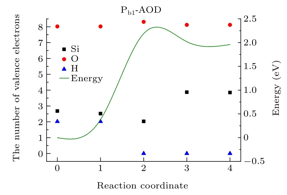
Fig. 7. Reaction curve of hole-induced depassivation of a Pb1-AOD defect in the SiO2/Si(100)interface(green curve). The black square,red circle and blue square mark the number of valence electrons in the active Si, O and H atoms,respectively.
3.2. Pb0 defect of the SiO2/Si(100)interface
The hole-induced depassivation reaction is simulated by the CI-NEB calculations, in which the initial and final states are introduced by structural optimizations(Fig.8). In the initial state (Fig. 8(a)), the length of the Si—H bond is 1.50 °A,and the distance between the H and O atoms is 3.82 °A (Table 3). The total number of valence electrons on the Si,H,and O atoms is 13.11. In the 01 state(Fig.9(a)),a hole is captured by the Pb0H defect, resulting in a reduction in the number of valence electrons on the Si atom to 1.98. So the 01 state can be regarded as the first step in hole-induced depassivation,and the reaction energy is about 0.15 eV.

Table 3. Number of valence electrons on the active atoms,the length of the Si—H and H—O bonds and system energy in hole-induced depassivation of a Pb defect.00,03,05 mark the initial,transition and final states,respectively.

Fig.8. Initial and final states of the hole-induced depassivation reaction of a Pb0 defect in the SiO2/Si(100)interface: (a)initial state;(b)final state.
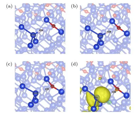
Fig.9.Intermediate states of the hole-induced depassivation reaction of a Pb0 defect in the SiO2/Si(100)interface:(a)01 state;(b)02 state;(c)03 state;(d)04 state.
As the reaction proceeds,in the 02 state(Fig.9(b))the defect center captures about 1.2 holes from nearby atoms again,so the 02 state can be regarded as the second step in holeinduced depassivation. The number of valence electrons on the H atom is reduced to 0.8,indicating that the Si—H bond is weakened and about to break. The energy of the system in the 02 state is 0.91 eV (Fig. 10), a moderate increase compared with the previous state.
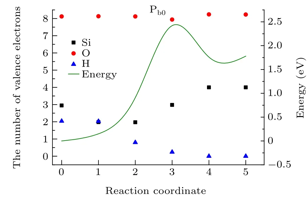
Fig. 10. Reaction curve of hole-induced depassivation of a Pb defect in the SiO2/Si(100) interface (green curve). The black square, red circle and blue square mark the number of valence electrons in the active Si,O,and H atoms,respectively.
Unlike the previous reactions of the Pb1-bridge defect and the Pb1-AOD defects, the PbH defect has already captured about 2 holes before the Si—H bond breaks. Hole trapping can influence the local structural parameters.[32]In addition,the Pbdefect is located at the second layer of the Si side, so the Pb0defect is relatively more compactly surrounded than the other defects and the structure around the Pbdefect is similar to that of crystalline silicon[42,43]so that the holes are captured by the PbH defect in advance to break the Si—H bond and release a proton.[44]
In the 03 state(Fig.9(c)), the H atom detaches from the Si atom with a distance of 2.12 °A and the O—H bond is not yet established. In this state, charge transfer takes place and the number of valence electrons on the H atom decreases to 0.24 while that on the Si atom increases by about 2.98. Because the Si—H bond is broken, the system energy is maximized(2.42 eV)at this state.
In the 04 state(Fig.9(d)),the proton detaches completely from the Si atom and bonds with the O atom. Compared with the previous state, this state traps about 1.08 electrons in the defect center,leaving a dangling bond of the Si atom with an unpaired electron,which can be marked as the third step in the hole-induced depassivation reaction.
In the final state (Fig. 8(b)), the proton detaches completely from the Si atom to a distance of 3.66 °A,and the length of the H—O bond is 0.98 °A.In addition,the total number of valence electrons on the Si,H and O atoms is 12.23,a decrease of about 0.88 compared with the initial state. This is equivalent to consuming 0.88 holes in the whole reaction. At the end of the reaction,the Pbdefect is reactivated to a neutral state with an unpaired electron. The energy of the final state is 1.78 eV,which is 0.42 eV lower than that of the transition state.
3.3. Pb defect of the SiO2/Si(111)interface
The pathway between initial and final structures(Fig.11)is simulated by CI-NEB calculations. In the 00 state(Fig. 11(a)), the total number of valence electrons on the Si,O, and H atoms is 12.97. From the 00 state to the 02 state(Fig.12(b)),the length of the Si—H bond increases from 1.50 °A to 1.54 °A, and the distance between the H and O atoms decreases by 25.68%.

Fig.11. Initial and final states of the hole-induced depassivation reaction of a Pb defect in the SiO2/Si(111)interface: (a)initial state;(b)final state.

Fig. 12. Intermediate states of the hole-induced depassivation reaction of a Pb defect in the SiO2/Si(111)interface: (a)01 state;(b)02 state;(c)03 state;(d)04 state.
In state 02(Fig.12(b)),compared with the previous state,the PbH defect center captures 0.88 holes and the number of valence electrons on the Si atom decreases to 2.23. This state can be considered as the first step in the hole-induced depassivation reaction. Since the Si—H bond has not been broken,the energy is only 0.46 eV,slightly higher than the initial state.
As the reaction proceeds,the H atom moves toward the O atom and the energy of the system increases(Fig.13). In state 03(Fig.12(c)), as shown in Table 4, the H—O bond develops after the Si—H bond has broken. Compared with the previous state, the defect center captures about 1.57 holes again,and the number of valence electrons on the H atom reduces to 0.64. Because the activated defect center captures the hole again,the transition state(03 state)can be regarded as the second step in hole-induced depassivation. Like the hole-induced depassivation of the Pb1-bridge defect and AOD defect,in the second step the Si—H bond breaks leaving a dangling bond of the Si atom with two positive charges; moreover, the system energy is about 1.76 eV,reaching a maximum(Fig.13).

Table 4. Number of valence electron on the active atoms,the length of the Si—H and H—O bonds and system energy in hole-induced depassivation of a Pb defect.00,03,05 mark the initial,transition and final states,respectively.

Fig. 13. Reaction curve of hole-induced depassivation of a Pb defect in the SiO2/Si(111) interface (green curve). The black square, red circle and blue square mark the number of valence electrons in the active Si,O,and H atoms,respectively.
In the final state(Fig.11(b)),the number of valence electrons on the Si atom increases to 3.86 due to electron trapping and the passivated Pbdefect is reactivated,so that this step can be considered as the third step of the hole-induced depassivation reaction. In this step,H+is connected to the O atom at a distance of 1.00 °A. Furthermore, the system reaches equilibrium with an energy of 1.13 eV,which is 0.63 eV lower than that of the saddle point. At this point,the total number of valence electrons on the Si, O, and H atoms is 12.10, which is about 0.87 electrons less than in the initial state, which indicates that a hole is consumed in the whole reaction.
According to Ref.[10],holes are not as efficient as electrons at causing interface damage. In fact, for a NMOSFET,at low gate voltage only hole injection can produce interface states.[45,46]Jechet al.just considered the separate effect of holes and electrons on the interface; however, in their work, more than one hole was trapped by the defects during the reaction, resulting in breakage of the Si—H bond. In the hole-induced depassivation reaction, an interface trap finally appears due to the combination of electrons with previously trapped holes. In addition, experimentally it was found that carriers with energies between 2 eV and 5 eV can still excite the vibrational states of the Si—H bond. In this work, the average barrier of the hole-induced depassivation reaction is 2.20 eV which agrees well with the experimental data of the dissociation kinetics according to Refs.[5,17],so is sufficient to break the Si—H bond.
4. Conclusion and perspectives
In this work,to investigate the hole-induced depassivation reaction(HPb+h→Pb+H+)of four interface defects,the Pbdefect in an a-SiO2/Si(111)interface and the Pb1-bridge,Pb1-AOD and Pb0defects in an a-SiO2/Si(100)interface have been introduced. The transition states and barriers are obtained via the CINEB method to simulate the process of the reaction.The Bader charge method is used to analyze the evolution of the number of valence electrons on the active atoms(the Si,H,and O atoms). Finally,the general mechanism of the hole-induced depassivation reaction of Pb-type defects is found.
During the reaction,the number of valence electrons on O remained almost constant,and charge transfer occurs between Si and H atoms. In fact,in the process of the reaction,Pb-type defects may trap more than one hole. It is shown that the total number of valence electrons on the Si,H,and O atoms in the initial state is about 13,and in the final state it is about 12.
This research suggests that hole-induced depassivation of the defects in an a-SiO2/Si interface actually occurs in three steps. In the first step, a hole is captured by the saturated defect.In this step,the Si—H bond is stretched but not yet broken,indicating that the system becomes unstable so the reaction will continue. In the second step,one more hole is trapped by the PbH defect center. At this point, the Si—H bond breaks,leaving a three-coordinated Si atom with positive charge. In addition,for the Pb1-bridge,Pb1-AOD and Pbdefects,the second step in depassivation is the transition state of the depassivation reaction,in which the system energy reaches its maximum.
However,before the Si—H bond is broken and the depassivation reaction reaches the transition state, the Pb0defects capture one more hole. The calculated reaction steps of the Pb0defect are different from those of the other defects,possibly because the Pb0defect is located in the second layer from the top of the unoxidized monolayer of the Si side in which the Pb0defect is relatively more compactly surround than the other defects, so that a second hole is required in advance to break the Si—H bond.
Finally, in the third step of the hole-induced depassivation reaction,the Si atom captures an electron and the Si atom becomes neutral. In this step, a neutral Pb-type defect with a dangling bond is formed, implying that the Pb-type defect is reactivated. In the final stage of the depassivation reaction,due to the conservation of charge,the total number of valence electrons on the Si, O, and H atoms is about 1 electron less than in the initial state, indicating that a hole is consumed in the whole reaction. This study will help us to understand the mechanism of the hole-induced depassivation reaction of the defects in an a-SiO2/Si interface from a microscopic point of view.
Acknowledgments
Project supported by the Science Challenge Project(Grant No.TZ2016003-1-105),Tianjin Natural Science Foundation, China (Grant No. 20JCZDJC00750), and the Fundamental Research Funds for the Central Universities—Nankai University(Grant Nos.63211107 and 63201182).

- Chinese Physics B的其它文章
- Erratum to“Boundary layer flow and heat transfer of a Casson fluid past a symmetric porous wedge with surface heat flux”
- Erratum to“Accurate GW0 band gaps and their phonon-induced renormalization in solids”
- A novel method for identifying influential nodes in complex networks based on gravity model
- Voter model on adaptive networks
- A novel car-following model by sharing cooperative information transmission delayed effect under V2X environment and its additional energy consumption
- GeSn(0.524 eV)single-junction thermophotovoltaic cells based on the device transport model