
Improving the surface insulation of epoxy resin by plasma etching
2021-09-10 09:26:42HuijuanRAN冉慧娟YanzeSONG宋巖澤JiyuanYAN閆紀(jì)源HongliangLIAN廉洪亮YuchanKANG康玉嬋ChengkaiPENG彭程凱andQingXIE謝慶
Plasma Science and Technology 2021年9期
關(guān)鍵詞:洪亮
Huijuan RAN (冉慧娟),Yanze SONG (宋巖澤),Jiyuan YAN (閆紀(jì)源),Hongliang LIAN (廉洪亮),Yuchan KANG (康玉嬋),Chengkai PENG (彭程凱)and Qing XIE (謝慶)
State Key Laboratory of Alternate Electrical Power System with Renewable Energy Sources,North China Electric Power University,Beijing 102206,People’s Republic of China
Abstract Epoxy resin(EP)tends to accumulate a large amount of charge on its surface when exposed to a high-voltage DC electric field,which leads to a reduction in its insulative performance and an increase in potential safety risks in power systems.To suppress charge accumulation,improve the flashover voltage of the EP,and reduce the risk of gas insulated switchgear (GIS) / gas insulated transmission line (GIL) failure,we used two plasma-etching methods,i.e.,atmospheric-pressure dielectric barrier discharge(DBD)and the atmospheric-pressure plasma jet(APPJ),to modify the surface of the EP.The surface morphology and electrical properties of the modified materials were explored as a function of time.The results show that after DBD treatment,the roughness of the sample increases by 103.9 nm,the conductivity increases by 3.9×10⁻¹⁸ S,and the flashover voltage increases by 14.4%; after APPJ treatment,the roughness of the sample increases by 223.5 nm,the conductivity increases by 3.4×10⁻¹⁷ S,and the flashover voltage increases by 18%.This shows that both plasma-etching methods can improve the insulation properties of materials by improving the surface-charge characteristics.The two methods are compared with each other: the APPJ treatment method is better at improving the surface roughness and electrical properties of materials,and this flexible treatment method has greater potential in industrial applications.
Keywords: plasma,epoxy resin,physical etching,surface morphology,electrical properties
1.Introduction
Low-temperature non-equilibrium plasma can be produced by applying an electric field using a power-frequency supply,a high-frequency and high-voltage power supply,or nanosecond pulse power supply to produce discharge in a certain gas space.Low-temperature plasma technology is widely used in surface modification,ozone generation,waste gas treatment,and other fields[1,2].Plasma surface modification only affects the physical and chemical properties of the treated parts,but does not damage the internal structure of the materials.Compared with traditional modification methods,plasma surface modification is more efficient and environment friendly,which thus attracts an increasing amount of research attention in the field of materials modification.
The main gas-discharge methods of producing plasma are coronal discharge,glow discharge,arc discharge,dielectric barrier discharge (DBD),and the atmospheric-pressure plasma jet(APPJ)[3].Borciaet almodified the surfaces of two materials with a spiral-electrode DBD in the air and found that short-duration DBD treatments (less than 1 s) can significantly change the surface characteristics of the samples in a uniform manner.With an increase in the treatment time,the surfaces of the tested materials oxidized and the contact angle decreased [4].Zhanget alused atmospheric-pressure air DBD to modify the surface of a polyimide film for various application times,and found that polar functional groups were introduced on the surface of the film.With an increase in the modification time,the surface conductivity gradually increased,while the corona-resistance time of PI film first increased and then decreased.When the modification time was 10 s,the corona-resistance time was maximized [5].Zhanget alused He/CF4to modify the surface of EP by the APPJ method.The results showed that the surface roughness of EP increased after treatment.Given an appropriate treatment time,the flashover voltage of an EP sample could be increased by 30%–50%.They believed that the main reason for the improvement in insulation performance was related to the change of surface roughness and the access to fluorine groups[6].Liuet alused a glow-discharge plasma to modify the surface of biaxially oriented polypropylene (BOP) for biological use and studied the influence of various plasma parameters on its surface properties.They found that the hydrophilicity,active chemical functional groups and surface structure of the film were all significantly changed after plasma modification [7].The induced modification of the surface was not permanent,since the surface tended to recover to its untreated state.Morentet alstudied the aging of polypropylene (PP) and polyethylene terephthalate (PET)films and treated them with a dielectric barrier discharge operating at a medium pressure (5.0 kPa) in air,helium,and argon.The results showed that the working gas used during the plasma treatment has a significant influence on the aging processes of both PP and PET films [8].Zhanget alused three methods to improve the surface-charge dissipation properties of epoxy resin insulators.The results showed that the introduction of SiOxand C-Fnfunctional groups improved the anti-aging properties of the DBD-treated and fluorinated samples [9].Liet aldescribed the development histories of the functionally graded materials(FGMs)applied in electrical engineering and the related optimization methods in detail.The field-regulation effects and fabrication technologies of different FGM insulators were also compared.To overcome the limitations of traditional FGM insulators,the surface FGM(SFGM)design was proposed,and preparation methods and the electrical performance were demonstrated [10].
A large number of scholars have researched the influence of a material’s surface morphology on its electrical properties.Wuet almodified the surface of titanium dioxide sputtered from aluminum,copper,and stainless steel by the vacuum sputter-coating method,and found that the breakdown voltage of the liquid dielectric was significantly increased after the treatment[11].Xieet alcarried out vacuum surface-flashover experiments on EP under various electric fields,and described the relationship between the dielectric surface-insulation characteristics and the surface roughness/fractal parameters[12].Zhanget alused laser etching and sandpaper grinding to form regular pits on a ceramic surface,and manipulated its flashover characteristics through surface roughness [13,14].Langet alcarried out a surface-flashover experiment using poly methylmethacrylate (PMMA) in vacuum; the results showed that with an increase in the surface roughness,the flashover voltage of PMMA first decreased and then increased[15].Xueet alused sandblasting technology to treat the semisurface roughness of an insulator,and found that this surface roughness treatment could inhibit the surface-charge accumulation and improve the flashover performance on the surface of the insulator [16].
A large number of studies [17–22] have shown that changing the surface physical morphologies of insulating materials can affect the dynamic characteristics of surface charge,and thus modify their insulation characteristics.Liet alobtained the parameters of charges trapped on the surfaces of polytetrafluoroethylene,quartz,and alumina by surface-charge measurement and thermally stimulated current measurement.It was found that surface-charge trapping has a significant influence on the uniformity of the discharge [23].Nikonovet alexamined the discharge behavior of short metallic–dielectric electrode gaps in air at atmospheric pressure as a function of the surface-charge density on a dielectric anode.The results indicated that surface-charge accumulation,as a consequence of successive discharges with the same polarity,appreciably influenced the photon flux at the cathode and the photoionization rate in the gas volume[24].Liuet alstudied the effects of DBD plasma and radio-frequency (RF)plasma on the surface wettability,chemistry,and microstructural changes of the surface of polytetrafluoroethylene(PTFE) using a comparative method.Both types of plasma could significantly improve the PTFE surface wettability owing to the changes in the surface chemistry and the surface microstructure [25].However,different treatment methods caused different etching results on the surfaces of samples.For this reason,we constructed a plasma surface-modification platform,a surface-charge measurement platform,and a surface-flashover-voltage measurement platform.Using argon as the working gas,we etched EP surfaces by DBD and APPJ at atmospheric pressure.The surface properties of the samples,including the surface physical morphology and the electrical properties,were characterized,and the influence of surface roughness on the flashover performance of EP was explored.
2.Experimental device and test platform
2.1.Experimental platform and methods of plasma modification
2.1.1.Plasma surface modification platform.The modified platform is shown in figure 1.The DBD platform consists of a power supply,a mass flowmeter,a mass flow controller,a DBD reactor,a measuring capacitor,an oscilloscope,a shielding box,and other components.The output voltage range of the DC power supply used in the experiment is from 0 to ?50 kV.The flashover voltage was measured by a highvoltage probe (Tektronix,P6015A,1000:1) and the surface discharge current was measured by a current coil (Pearson,model 6585,1 V/A).The signals collected by the probe and coil were sent to the oscilloscope (Tektronix DPO 2002B)through a coaxial cable.The sampling frequency and bandwidth were 1 GHz and 200 MHz,respectively.The voltage-edge trigger mode was used to capture and record the discharge voltage and current waveform at the time of surface flashover.In order to protect the experimental equipment,a 1 MΩ current-limiting resistor was connected in series in the experimental setup.The APPJ platform was similar to the DBD platform,except that the DBD reactor was replaced by an APPJ jet array.The shielding box was made by the research team and was filled with argon before the experiment to avoid the influence of atmospheric oxygen and water.The jet array consisted of four jet units arranged in a 2×2 square,with an outer diameter of 8 mm and an inner diameter of 4 mm.The purity of the argon used in this experiment was 99.999%.

Figure 1.DBD (a) and APPJ (b) plasma surface-modification platforms.
2.1.2.Experimental parameters and treatment methods.Before using the plasma surface-treatment platforms shown in figure 1 to modify the material,it is necessary to optimize the selection of discharge parameters,and comprehensively consider the power energy and discharge uniformity.The optimization was done in advance.Combined with the experimental data from our research group,a power-supply voltage of 6–7 kV,a current of 1 A,and an argon flow rate of 4 l min?1were selected for DBD.A power-supply voltage of 4.5 kV,a current of 2 A,and an argon flow rate of 5 l min?1were selected for APPJ.During the jet discharge,the discharge was stable and the arc appeared as a blue-topurple light without obvious discharge filaments.
The EP surface plasma treatment steps are as follows:
(1) The untreated EP was placed in an ultrasonic cleaning machine and cleaned with deionized water,acetone,and pure ethanol for 3 min,and then dried in a drying oven for 25 h.
(2) The EP was placed on the atmospheric-pressure DBD(or APPJ) low-temperature plasma surface-treatment platform,the samples were placed in the treatment center,and the power supply voltage,current,and discharge spacing were adjusted.
(3) During the modification,the discharge uniformity and gas flow uniformity were maintained,and the discharge voltage and current amplitude were read using the oscilloscope.
(4) The plasma application time was pre-set and the modified sample was taken out after the discharge.
2.2.EP surface electrical performance test platform

Figure 2.Experimental platform for surface flashover.
2.2.1.Experimental platform for surface flashover.The experimental platform for the surface flashover on epoxy resin materials consists of the experimental chamber,experimental electrode,high-voltage DC power supply,multi-function oscilloscope,high-voltage probe,and other devices.A schematic diagram of the experimental device is shown in figure 2.The flashover experiment is conducted at 24°C at a relative humidity of 30% under standard atmospheric pressure.The uniform-boost method is adopted during processing,i.e.the voltage is ramped at a constant rate of 0.5 kV s?1until flashover occurs.The experiment is repeated 15 times at 2 min intervals,and the average value of the flashover voltage is calculated.Needle electrodes are used in the experiment.The tail of the needle electrode is semicylindrical,with a diameter of 4 mm at the bottom and a total length of 15 mm.The tilt angle of the electrode tip is around 15 degrees and the distance between the two electrodes is 7 mm.The high-voltage DC power supply has an output range of 0 to ?50 kV and is manufactured by Dongwen High Voltage Power Supply (TianJin) Co.Ltd.The multi-function oscilloscope (Tektronix DPO),is supplied by Ocean Instruments Co.Ltd.The discharge chamber is made of stainless steel and is cylindrical in shape.A detachable quartz glass window is set on the upper surface and in front of the chamber,which is convenient for observing the experimental phenomena in a vacuum.In addition,the cavity is also equipped with a two-dimensional operating device,which has a scale to accurately control the distance between the two electrodes and the height of the sample table.

Figure 3.Surface potential test platform.
2.2.2.Surface potential test platform.A schematic diagram of the surface potential test platform is shown in figure 3.The main equipment includes the high-voltage DC power supply,a charging needle,an electrometer,a data-acquisition card,a supporting computer and software,etc.The electrometer is made by Trek company of USA (P0865).The stainless-steel needle electrode is 10 cm long and has a 25 μm radius of curvature.The needle is connected to a high-voltage DC power supply,and placed above the sample for charging.The plate electrode is 1 mm thick and made of aluminum.It is placed on the experimental platform and grounded.The stepper motor control box is manufactured by Beijing Lianying Precision Machinery Co.Ltd.,and the model is ZK200.It is connected to the computer through a USB cable.Through computer programming,combined with the matching potential measurement probe control software,the control device can drive the electrostatic probe to move in theX-Ydirection along the sample’s surface.Information about the potential at the measuring point is transmitted to the electrometer and output to the dataacquisition card,and finally the data are stored in the computer.
In order to study the charge dissipation characteristics of the EP surface,it is necessary to charge the sample first,to create surface charges.The main surface-charging methods include coronal discharge,electron-beam charging,and contact charging.In this experiment,a needle–plate-electrode coronal discharge was used to charge the samples.The charging system is composed of a high-voltage power supply and a charging needle.The tail end of the stainless-steel charging needle is connected to the output of the high-voltage power supply and the sample is placed on the grounded aluminum plate; the charging needle can be adjusted to a position 5 mm above the center of the sample.After charging,the sample is moved to the surface potential test platform,the acquisition card is turned on and the surface potential test can be started.Single-point continuous acquisition is used in this experiment,that is,the probe is aimed at the position of the charging needle,and the potential data are continuously collected from 0 to 30 min.The surface-charge dissipation rate of the EP material is the ratio between the potential difference at the beginning and end of the measurement and the initial potential.The calculation formula is shown in (1):

whereLis the surface-charge dissipation rate,Vt0is the surface potential at the beginning of the measurement,andVtis the surface potential at the end of the measurement.For the convenience of calculation,the normalized surface potential data can be obtained by dividing the surface potential at each time and the initial potential of the EP sample.The data can also be used for the calculation of dissipation characteristics.
2.2.3.Surface conductivity test platform.The surface conductivity test platform is composed of a high-resistance meter,a measuring electrode,a data-acquisition card,and a computer.The high-resistance meter (model SM7110),measuring electrode (model SME-8311),data-acquisition card (Z5010),and supporting computer software produced by the Hoki company of Japan can quickly detect the surface conductivity of samples,due to their measurement stability and strong resistance to interference.
During the measurement,the sample to be measured is placed in the shielding box of the measuring electrode,the RS surface conductance measurement mode is selected,the power-supply voltage is set to 1 kV,and the measurement results are transmitted to the computer through the acquisition card and can be obtained after software processing.The slow measurement speed is selected,which is 2000 measurements per 300 ms.The average value of the last 500 measurements is calculated and used as the surface conductivity of the sample.
3.Effect of DBD etching on the electrical properties of the EP surface
3.1.Surface morphology after DBD etching
The EP surface plasma-etching experiment was carried out under atmospheric pressure at room temperature.Ar was used for the atmospheric-pressure plasma etching.The surface morphology and conductivity of the EP were analyzed before and after modification.Five groups of EP samples,distinguished by the plasma energy power and discharge uniformity used,were treated for 1–5 min.The results of the high-pressure experiment are affected by many factors,such as temperature,humidity,and pressure.Therefore,the results are characterized by dispersion and randomness.To avoid this unwanted influence,six samples were processed for various amounts of time varying from 0 to 5 min,and each sample was repeatedly measured 15 times.The final result in the table is obtained by averaging 90 experimental data points.The surface morphology and roughness of the treated samples were tested using a surface profiler (contour GTK).
From figure 5,it can be seen that after DBD treatment at atmospheric pressure,the surface impurities of the EP sample were removed,and some granular protrusions were generated[21],which increased the surface roughness.With increasing modification times,the density of granular protrusions on the surfaces of the EP samples increased,especially when the modification time was 4 min.When the treatment time was more than 2 min,the size of the protrusions on the surface of the EP sample also increased.
The surface roughness of the EP samples after DBD etching (represented by the arithmetic mean deviationRaofthe surface profile)is shown in table 1.It can be seen that the surface roughness increased with increasing of EP surface modification times.When the modification time was 1 min,the surface roughness clearly increased,and then the increase rate slowed down.After 3 min,the increased rate of surface roughness rose again,and the increase ofRareached a maximum when the modification time was 4 min.
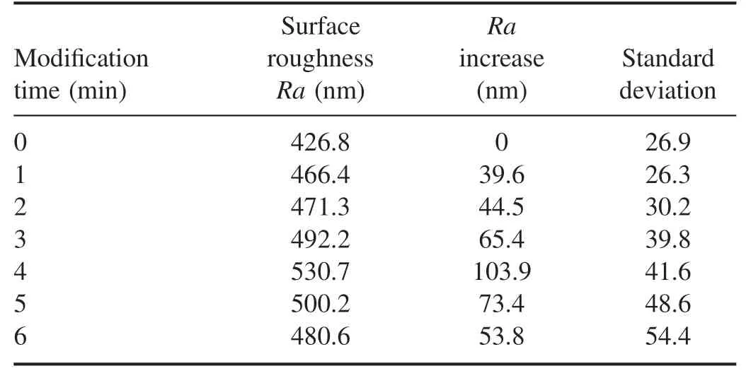
Table 1.Surface roughness of EP samples after DBD etching.

Table 2.Surface conductivity of EP samples after DBD etching.
3.2.Electrical properties after DBD etching
The surface of the EP sample was modified by DBD with Ar.The values of surface conductivity before and after treatment are shown in table 2.The surface conductivity of the EP sample was tested after plasma physical etching from 48 to 72 h.It can be seen that the surface conductivity of the sample increased slightly during the first 4 min of treatment time,and decreased after reaching a maximum value at 4 min of treatment time.At the end of the treatment,the value was still higher than the surface conductivity of the sample before treatment.During the whole modification process,the surface conductivity was improved by less than an order of magnitude.According to the analysis of the results in section 3.1,we conclude that the surface conductivity is affected by the roughness.With an increase in the treatment time,the surface roughness of the EP samples gradually increases,and the surface conductivity increases.
Figure 4(a)shows the normalized attenuation data of the single-point surface potential within 30 min after powering off the DBD etching.It can be seen from figure 4(a) that in the initial stage of the modification,the charge dissipation rate increased slightly.When the modification time reached 4 min,the surface charge decayed exponentially.When the modification time increased to 5 min,the charge dissipation rate first increased and then decreased exponentially.In the beginning,it decayed exponentially,and then gradually slowed down.
It can be seen from figure 4(b)that with an increase in the modification time,the depth of the charge traps on the surface of the EP sample gradually became shallower.When the time increased to 3 min,the surface-charge-trap distribution curve showed two characteristic peaks,and the peak of trap energy level density decreased.With an increase in the modification time,the depth of the trap energy level continued to decrease,reaching 0.952 eV at 5 min.However,when the modification time increased to 6 min,the trap energy level increased.
The surface-flashover voltages of EP samples treated by atmospheric-pressure DBD were tested,and the results are shown in figure 5.When the treatment time was 5 min,the flashover voltage increased from 10.44 kV at 4 min to 10.79 kV,which was 14.4% higher than that of untreated samples.The flashover voltage of the sample with a modification time of 6 min is lower than that with 5 min of modification,but it is still higher than that of the untreated sample.
4.Effect of APPJ etching on the electrical properties of the EP surface
4.1.Surface morphology after DBD etching
Similarly,the surface morphology and roughness of the EP samples modified by APPJ in the Ar atmosphere were tested.There were a few scattered sharp protrusions on the surface of the untreated EP.With an increase in the modification time,the granular protrusions on the surface of the EP gradually became dense.These protrusions are at the nanoscale,which led to an increase in surface roughness.When the modification time was 4 min,the plasma-etching effect on the EP surface was very obvious.
Table 3 shows the EP surface roughness before and after APPJ treatment.Compared with the DBD treatment,the surface roughness of the APPJ treatment shows the same increasing trend,and the amplitude is larger.It can be seen that the plasmajet treatment increases the surface roughness of the sample,which is caused by plasma etching of the EP surface.
4.2.Electrical properties after APPJ etching
Table 4 shows the change in the surface conductivity of the EP after the surface modification of APPJ in Ar atmosphere.It can be seen from table 4 that the surface conductivity of EP increases with an increase in the treatment time.When the treatment time was 4 min,the surface conductivity of the EP increased to 4.0×10?17S.When the treatment time was 5 min,the surface conductivity of EP decreased.During the whole process,the surface conductivity of the EP increased by nearly an order of magnitude,and the trend of the change was similar to that of DBD etching.
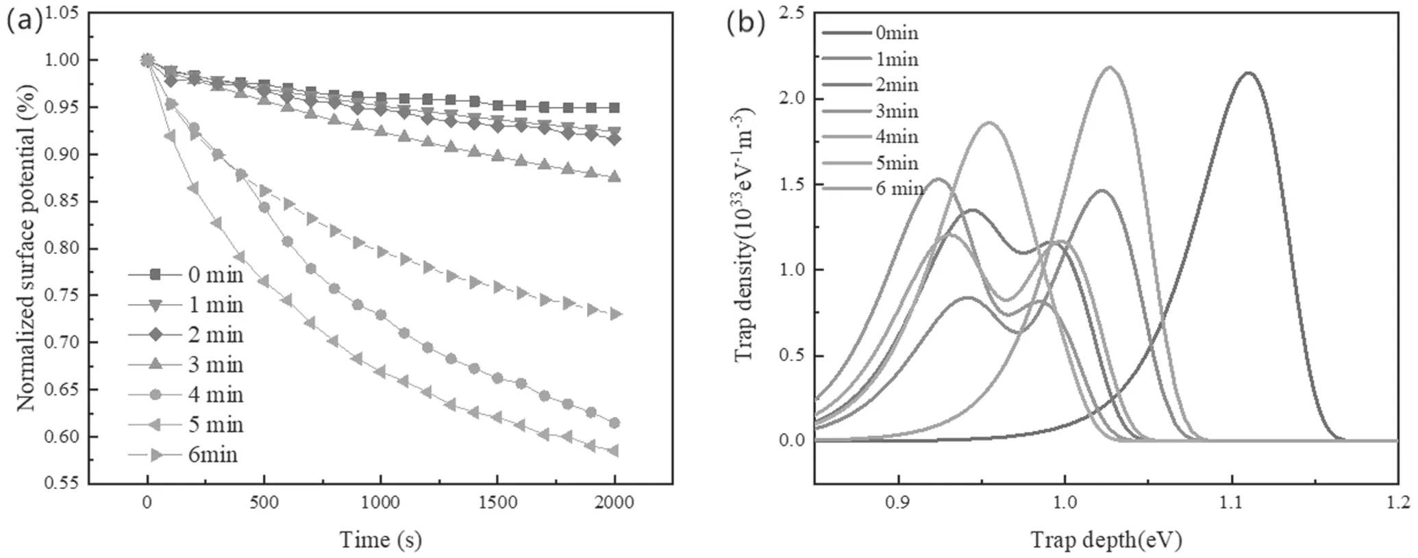
Figure 4.Normalized dissipation curve (a) and trap distribution curve (b) of EP after DBD treatment.

Figure 5.Flashover voltages of EP samples after DBD etching.

Table 3.Surface roughness of the EP samples after APPJ etching.
Figure 6 shows a comparison between the surface potential attenuation and the trap density of the samples before and after the plasma-jet treatment.It can be seen from figure 6(a)that with an increase in the modification time,the surface-charge dissipation rate of the EP gradually increased.When themodification time was 3 min,the surface-charge dissipation rate of EP was obviously accelerated,and the surface-charge dissipation rate decreased exponentially at the beginning and slowed down in the later stage.The charge dissipation rate of EP samples after 4 min of modification was slightly higher than that of EP samples after 3 min of modification.When the modification time of the EP increased to 5 min,the surface-charge dissipation rate decreased.This is consistent with the change in the surface charge of the EP samples treated by DBD.It can be seen from figure 6(b) that with an increase in the modification time,the plasma treatment has a significant shallowing effect on the depth of the surface-charge-trap energy level of the EP,which is in good agreement with the variation trend of the surface potential normalized dissipation curve.

Table 4.Surface conductivities of EP samples after APPJ etching.
In order to further study the influence of EP’s surface micromorphology on its electrical properties,the surfaceflashover voltage of the samples was tested,and the results are shown in figure 7.It can be seen from figure 7 that the surface-flashover voltage of the EP sample obviously increased in the first minute of APPJ treatment.With an increase in the treatment time,the surface-flashover voltage continued to rise.When the treatment time reached 4 min,the surface-flashover voltage increased to 11.03 kV,which is about 18%higher than that of the untreated sample.When the treatment time was 5 min,the surface-flashover voltage decreased,but its value was still higher than that of the untreated samples.

Figure 6.Normalized dissipation curve (a) and trap distribution curve (b) of the EP after the APPJ treatment.

Figure 7.Flashover voltages of EP samples after APPJ etching.
5.Analysis of the results
5.1.Comparison of the electrical performances of DBD and APPJ treatments
The variation of EP surface roughness with treatment time for the two plasma modification methods is shown in figure 8.It can be seen from figure 8 that both plasma modification methods can improve the surface roughness of EP.After the APPJ treatment,the roughness of the EP was significantly higher than that due to the DBD treatment.
The increase of the surface roughness of EP reduces the accumulated charge on the surface area,thus improving the electrical performance of the EP.Figures 5 and 7 show the variation of the surface-flashover voltage of the EP as a function of the treatment time for the two treatment modes.It can be seen from figures 5 and 7 that the electrical performance of the EP after APPJ treatment is better than that following DBD treatment,which is consistent with the trend of surface roughness.According to the calculation of the surface area of EP samples and the power during the plasma treatment,the power density during the APPJ treatment is about twice as large as that of the DBD treatment.This result indicates that the plasma discharge power density may be one of the factors leading to the better effectiveness of the APPJ treatment.

Figure 8.Change of surface roughness.
5.2.Surface morphology and charge dynamic characteristics
In a certain gas environment,a low-temperature non-equilibrium plasma can be produced by applying an electric field to generate a discharge,which can be used for surface modification [26,27].In the process of plasma surface modification,a variety of particles are excited to absorb energy and become high-energy active particles.A large number of high-energy particles are carried by the pure Ar gas stream to impact and react with the sample’s surface.The changes mainly include three aspects: (1) surface cross-linking; (2)introduction of polar functional groups; (3) surface etching.Surface etching forms a series of undulating etching areas on the sample’s surface,resulting in an increase in the EP surface roughness.
A large number of scholars believe that [28] the accumulated charge in the gas–solid interface area mainly arises in three ways: gas-side conduction,solid-side conduction,and solid-surface conduction.The contribution of these three factors to the surface-charge densityρscan be expressed as follows:
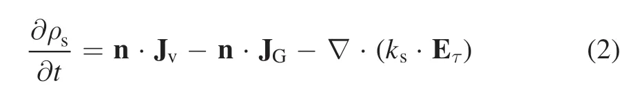
where Jvand JGrepresent the solid-side current and gas-side current flowing into or out of the insulator’s surface,respectively; Jvis determined by the solid conductivity and the electric field strength in the solid;JGis determined by the gas conductivity and the electric field strength in the gas;ksis the surface conductivity of the insulator;τE is the tangential electric field component of the insulator’s surface; n is the unit normal phasor of the solid–gas interface.It can be seen from the previous analysis that a change in the EP surface morphology will lead to the change of electron behavior and electron motion path,which will,in turn,lead to a change of the surface conductivity,ks.An increase in the surface conductivity will reduce the charge accumulation on the surface of the material.
On the other hand,after plasma treatment,dense and tiny sharp protrusions appear on the surface of EP material,and the height of the granular protrusions remains at the nanometer level.At this time,the surface of the EP material has a high-density,rough,and nearly uniform plasma-etched morphology.Due to the limitations of the manufacturing process and mold precision,untreated samples always have surface defects.Local defects distort the electric field strength and cause local coronal discharge or even breakdown.These phenomena lead to a large number of free charges in the air gap near the defect,which move towards the EP surface under the action of the electric field and eventually accumulate on the EP surface.In the plasma-etching state,a DC voltage is applied to the two ends of the material to form a surface electric field.Compared with the untreated sample,the uniformity of the surface electric field is improved and the distortion of the local electric field is reduced.The uniform field avoids the occurrence of partial discharges under high electric fields and reduces the number of free charges near the surface of the sample,thus inhibiting the accumulation of surface charges.
5.3.Surface morphology and flashover voltage
The surface-flashover voltage of EP can be affected by plasma etching.According to the test results for the flashover voltages of samples under the two treatment methods,the flashover voltage along the surface of EP is positively correlated with its surface roughness.This paper mainly explains this observation from two perspectives,as follows.

Figure 9.Schematic diagram of mountain-like folds.
First of all,considering a cross-section between the cathode and the ground electrode,an increase in the roughness will cause mountain-like folds between the two electrodes,as shown in figure 9.Similar to the application principle of of an insulator’s umbrella skirt,the appearance of mountain-like folds from a micro angle will increase the movement path of electrons that are emitted from the cathode along the ground electrode’s surface,which is equivalent to increasing the creepage distance of electrons in the flashover process.With an increase in the creepage distance,the emitted electrons need to consume more energy to travel to the other electrode,and electrons without enough energy cannot complete the whole migration path.Therefore,an increase in the surface roughness will increase the surfaceflashover voltage of the EP material [13,14].
Secondly,according to the secondary-electron emissionavalanche model[29],the electrons emitted from the cathode move to the anode under the action of the electric field.During this movement,the electrons are accelerated by the electric field force,and their kinetic energy is increased as the speed increases.After the particles with high kinetic energy collide with the surface of the material,the energy is transferred to electrons on the surface of the material.These electrons are then stimulated to break away from their inherent trajectories and become free electrons,which are called secondary electrons.Due to the high electric field strength,a particle that accumulates a lot of kinetic energy can often excite multiple secondary electrons,which themselves also accelerate under the influence of the electric field,and excite more electrons,finally forming an electron avalanche.When the electron avalanche gradually advances to the anode,a flashover channel will be formed on the surface of the sample,which will eventually lead to flashover.The mountain-like folds in the plasma-etched area of the EP surface block the trajectories of the initial electrons and the secondary electrons.The secondary electrons are more likely to collide with the surface of the material and lose kinetic energy during the electric field acceleration.As the distance traveled by the electrons becomes shorter,the kinetic energy carried by electrons decreases,and fewer electrons can be excited.After the secondary electrons collide with the mountain-like material surfaces,diffuse reflection may occur,as shown in figure 10.The ejected electrons are mixed with the seed electrons,which can cause secondary-electron emission,and the proportion of effective electrons is reduced.The secondary-electron emissivity is shown in formula (3):

Figure 10.Schematic diagram of collisions between electrons and the material surface.

Table 5.Surface oxygen contents of EP samples after DBD and APPJ.

where δmax(θ) is the maximum secondary-electron emission coefficient at incidence angle θ,δmax(θ) is the maximum secondary-electron emission coefficient at incidence angle 0,Isis the smoothness of the material,and θ is the angle of incidence.It can be seen that when the surface of the sample is smooth,Isis larger and the secondary-electron emissivity is higher.An improvement in the surface roughness reduces the smoothnessIs,and,as a result,reduces the secondary-electron emission coefficient,suppressing the occurrence of secondary-electron avalanches,improving the surface condition of the sample,and increasing the flashover voltage.
The combined action of the two factors leads to an increase in the flashover voltage along the surface of the EP material.However,when the treatment time is too long,the surface of the material will be more strongly etched,and uneven cracks and protrusions may appear.The appearance of irregular areas leads to a variable surface roughness distribution of the material,and the surface-charge distribution also changes accordingly,resulting in serious local field distortion on the surface.In this case,the surface-flashover voltage decreases.
5.4.Surface chemical composition
In the plasma treatment process,high-energy plasma is carried by the argon gas stream and bombards the surface of the EP,destroying the original chemical bonds and inserting new functional groups to functionalize the surface of the sample.In this paper,argon is used as the working gas,the plasma surface modification is performed in the atmosphere,and O-containing functional groups are inserted into the surfaces of the EP samples.The change of surface oxygen content reflects the addition of O-containing functional groups.XPS test results are shown in table 5.
Under the two modification methods,DBD and APPJ,the O element content on the EP surface gradually increased,reaching a maximum when the modification time was 4 min,and decreased when the modification time was 5 min.This trend is consistent with the changing trend of the surface electrical properties of the composite materials mentioned above,so the addition of the O-containing groups improves the insulation properties of the EP surface.The difference from previous studies is that,compared with APPJ,the EP treated with DBD has more O-containing functional groups,while its electrical performance is less improved.Therefore,we can conclude that under pure-argon plasma etching,the surface morphology has a greater impact on the electrical properties of the EP sample surface.
6.Conclusions
To suppress charge accumulation,improve the flashover voltage of EP,and reduce the risk of GIS/GIL failure,the plasma pure Ar etching of EP described in this paper was carried out by atmospheric-pressure DBD and APPJ.This paper mainly discussed the effects of the surface roughness and oxygen content on the surface conductivity and flashover voltage.The physical and electrical characteristics of the sample surface before and after the modification were measured and compared,and the mechanism responsible for influencing the surface charge was analyzed.A complete investigation of the surface composition and surface structure could be done in the future.The conclusions are as follows:
(1) Surface modifications of EP by atmospheric-pressure DBD show that the surface roughness of the EP material first increases and then decreases with increasing modification time,and the maximum increase is 103.9 nm.The surface conductivity of the EP material increases by less than one order of magnitude,and the surface-flashover voltage of the EP material increases by about 14.4%.
(2) Using APPJ to modify the surfaces of the EP materials,the surface roughness also first increased and then decreased with increasing modification time,with a highest increase of 223.5 nm,and the surface conductivity increased by nearly an order of magnitude.When the modification time was 4 min,the surfaceflashover voltage of the EP material reached 11.03 kV,which is 18% higher than that of untreated material.However,when the modification time was 5 min,the flashover voltage decreased.
(3) The surface roughness of EP after APPJ plasma modification is larger than that after DBD modification.In addition,the improvement in the surface-flashover voltage is more obvious,i.e.the insulative performance is better.
(4) After plasma treatment,the surface roughness,conductivity,oxygen content,and trap distribution of the EP materials show strong consistency and correlation.As the surface roughness increases,the conductivity and oxygen content gradually increase,and the trap energy level becomes shallower.
(5) After plasma treatment,the surface of the EP material shows nanoscale dense sharp protrusions,and the surface becomes rougher.When the surface of the EP material is high-density,rough,and approximately uniform,it can be considered that the surface electric field distribution is uniform,and the amount of accumulated charges on the surface area of the material is reduced.The surface conductivity is improved,and the local electric field distortion is reduced.At the same time,with an increase in surface roughness,the creepage distance of the EP material’s surface increases,and the insulation performance of the EP is improved as well.
Acknowledgments
This work was supported by National Natural Science Foundation of China (Nos.51777076,51507066),the Fundamental Research Funds for the Central Universities(Nos.2019MS083,2018MS084),and the Self-topic Fund of State Key Laboratory of Alternate Electrical Power System with Renewable Energy Sources (Nos.LAPS202116,LAPS202103).
猜你喜歡
公民與法治(2023年1期)2023-03-31 06:03:32
Plasma Science and Technology(2021年11期)2021-11-30 08:28:44
Plasma Science and Technology(2021年6期)2021-06-21 02:00:34
Chinese Physics B(2021年4期)2021-05-06 08:54:46
文化產(chǎn)業(yè)(2020年15期)2020-07-22 12:00:12
華人時(shí)刊(2017年21期)2018-01-31 02:24:16
小學(xué)生學(xué)習(xí)指導(dǎo)(低年級(jí))(2017年4期)2017-02-17 02:34:54
河北書畫研究(2016年6期)2016-02-03 02:57:43
環(huán)球市場(chǎng)信息導(dǎo)報(bào)(2015年15期)2015-12-03 06:18:35
新疆石油地質(zhì)(2015年2期)2015-02-28 19:25:42
 Plasma Science and Technology2021年9期
- Plasma Science and Technology的其它文章
- Conceptual design and heat transfer performance of a flat-tile water-cooled divertor target
- Study of selective hydrogenation of biodiesel in a DBD plasma reactor
- Temporal and spatial study of differently charged ions emitted by ns-laser-produced tungsten plasmas using time-of-flight mass spectroscopy
- Analysis of the microstructure and elemental occurrence state of residual ash-PM following DPF regeneration by injecting oxygen into non-thermal plasma
- The low temperature growth of stable p-type ZnO films in HiPIMS
- Research on the method of dual-frequency microwave diagnosis of plasma for solving phase integer ambiguity