
Fabrication of GaAs/SiO2/Si and GaAs/Si heterointerfaces by surface-activated chemical bonding at room temperature*
2021-07-30 07:40:52RuiHuang黃瑞TianLan蘭天ChongLi李沖JingLi李景andZhiyongWang王智勇
Chinese Physics B 2021年7期
Rui Huang(黃瑞) Tian Lan(蘭天) Chong Li(李沖) Jing Li(李景) and Zhiyong Wang(王智勇)
1Institute of Advanced Technology on Semiconductor Optics&Electronics,Institute of Laser Engineering,Beijing University of Technology,Beijing 100124,China
2College of Microelectronics,Beijing University of Technology,Beijing 100124,China
Keywords: surface-activation bonding,energy-dispersive x-ray spectroscopy,intermix,point defects
1. Introduction
Gallium arsenide (GaAs) is an attractive semiconductor material with excellent physical, chemical and mechanical properties. Bulk GaAs is a direct bandgap semiconductor material with a cubic zinc-blende structure, a lattice constant of 5.6419 ?A and a bandgap of 1.428 eV at room temperature.[1]Due to the high electron mobility of GaAs,its electron mobility is about five times higher than that of Si,and its operational speed is much higher than those of Si devices, so it can be used to fabricate high-speed or microwave semiconductor devices.[2]GaAs is also used to make hightemperature-resistant,radiation-resistant or low-noise devices,near-infrared light-emitting diodes (LEDs) and laser diodes(LDs), as well as photocathode materials.[3-6]More importantly, it has become the basic material for the future development of ultra-high-speed semiconductor integrated circuits. Over the last ten years, with the development of molecular-beam epitaxy (MBE) and metal-organic chemical vapor deposition (MOCVD), it has become possible to fabricate heterojunction and superlattice structures on GaAs substrates. Power electronic semiconductor devices, such as high-power electron-mobility transistor(HEMTs)and heterojunction bipolar transistors(HBTs),have engendered broader prospects for the application of GaAs material.[7,8]
Traditional silicon-based substrates (such as SiO2-on-Si and Si) are suitable for micro/nano manufacturing technologies. The combination of single-crystal GaAs with silicon oxide can produce a GaAs-on-insulator(GaAsOI,GaAs/SiO2/Si)structure, which can replace the Si-on-insulator (SOI) structure, improve the modulation speed and reduce parasitic effects.[9]The formation of a GaAs/Si structure can create ohmic interfaces which are beneficial to the fabrication of Si-based GaAs solar cells.[10-12]When GaAs is epitaxially grown on the surface of a Si wafer at temperatures between 500°C and 700°C, crystal defects such as dislocations and cracks appear. These defects reduce the device’s lifetime and affect its performance. Surface-activated bonding (SAB) can overcome the difficulties caused by the lattice and thermal expansion coefficient mismatches.[13]Yeoet al.[14]reported that the highest bonding energy of GaAs/Si was 478 mJ/m2under Ar fast atom beam(FAB)treatment conditions of 30 s, 120 mTorr and 200 W. Additionally, in order to fabricate low-resistance GaAs/Si heterointerfaces, Yutaka Ohnoet al.[15]optimized the surface-activation bonding and subsequent annealing conditions. In this method, the wafer surface was irradiated by an FAB of Ar before bonding. Heterojunctions realized by SAB,such as Si/GaAs,[14]Si/InP,[16]Si/SiC,[17]Si/GaN,[18]GaAs/GaN,[19]LiNbO3/SiC,[20]and diamond/Si,[21]have been widely studied. In addition, the electrical properties of the bonding interface can be changed by annealing.[22]
Aberration-corrected scanning transmission electron microscopy (AC-STEM) can be used to study the nanostructures at the bonding interface. It has been reported that an amorphous-type transition layer can be observed at the bonding interface.[23,24]Although the electrical properties of the interface are likely to be strongly influenced by its chemical properties,[22]the chemical properties at the interface or the properties of the chemical atomic bonds have not been fully understood. Consequently, it is necessary to study the chemical properties of the chemical atomic bonds at the GaAs/SiO2/Si and GaAs/Si bonding interfaces at the atomic level.
In this work, bonding interfaces between GaAs/SiO2/Si and GaAs/Si have been realized by surface-activated bonding(SAB) and subsequent annealing at RT. The bonding rate is observed using scanning acoustic microscopy(SAM),and the nanostructure of the bonding interface is studied by transmission electron microscopy (TEM) and energy-dispersive x-ray spectroscopy(EDX).The thickness of the interface transition layer is estimated,and the atomic composition at the bonding interface of the sample is analyzed.
2. Experimental methods
2.1. Materials
In this work, 4-inch double-sided polished P-type Bdoped Si (100) wafers with a thickness of 525 μm are used.For the SiO2/Si substrate,a SiO2layer about 300 nm thick is thermally oxidized on the surface of the Si wafer. Four-inch N-type Si-doped GaAs(100)wafers with a double-sided polishing thickness of 625 μm are used in the study.Before wafer activation, all substrates are successively soaked and cleaned using ethanol and deionized water.
2.2. Surface activation and bonding procedures
The GaAs,Si,and SiO2/Si substrates are activated by an Ar fast-atom beam (FAB). When the air pressure in the vacuum chamber is reduced to 2×10⁻⁶Pa, different substrates are activated for 60 s by the inert Ar-FAB at a voltage of 2 kV and a current of 60 mA (with a corresponding dose of 2×10¹⁸atoms/cm2at the atomic energy of 2 keV). The Ar-FAB reaches the surface at an angle of approximately 45°. After activation,the substrates are placed in a wafer bonder(EVG 520,EV Group,Austria). Under high-vacuum conditions(below 5×10⁻⁵Pa) and at RT, the bonding force and time are 10 kN and 5 min,respectively.
2.3. Surface and interface characterizations
After bonding,GaAs/SiO2/Si and GaAs/Si bonded wafer pairs are observed using SAM (SAM 301, PVA TePla, Germany). The frequency is set to 250 MHz and the scanning speed is 5 mm/s. GaAs/SiO2/Si and GaAs/Si wafer pairs are cut into dies with sizes of 10×10 mm2. The GaAs/SiO2/Si and GaAs/Si dies are then further cut into 500×500 μm2square islets with a depth of 725 μm. The specific process flow is shown in Fig. 1. It can be seen from the inset that the GaAs remains attached to the top of the die. The dies are annealed at 200°C for 1 min. Cross-sectional samples are then prepared by double beam FIB/SEM (JIB-4700F,Japan). During the thinning of the wafers, a carbon layer is deposited on the top of the samples in order to protect the areas to be studied. Ga+ions are accelerated at 2-30 kV to suppress the defects at the interface caused by the FIB process. Scanning electron microscopy (SEM) provides evidence of the uniform thickness of the FIB samples at the interfaces. The structural properties and chemical composition of the interface are determined by high angle annular dark field (HAADF) and energy dispersive x-ray spectroscopy(EDX)using aberration-corrected TEM(JEM-ARM 300F,Japan). The surface roughness of the bonded surface is a key factor for direct bonding at RT.The surface roughness of the GaAs, Si, and SiO2/Si substrates after Ar-FAB treatment is measured by atomic force microscopy(AFM,Bruker,Germany). The scanning area of the AFM is 10×10 μm2,and the resolution is 256×256 pixels.
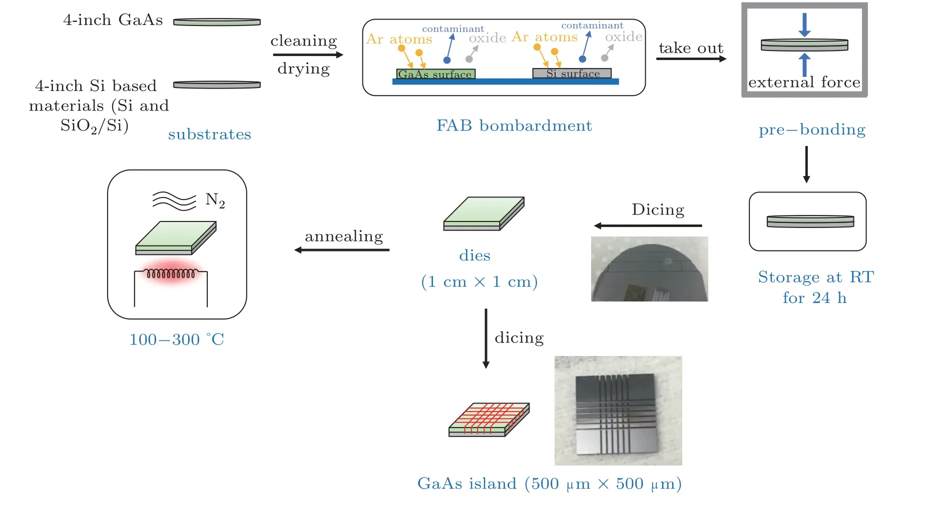
Fig.1. A schematic diagram of the bonding process using an Ar-FAB.
3. Results and discussion
3.1. Surface roughness after Ar-FAB treatment
As a key factor affecting the bonding quality at RT, the surface roughness of the bonding surface is directly related to the structural damage (cracks, bubbles, or holes) formed at the interface. A smooth wafer surface, with fewer defects induced by atomic bombardment and a surface saturated by-OH dangling bonds is favorable for direct bonding. The surface roughnesses of the GaAs, Si, and SiO2/Si substrates before and after Ar-FAB bombardment are measured by AFM.Figure 2 shows the AFM images and root-mean-square values(RMS)of the surface roughnesses of the GaAs,Si and SiO2/Si substrates after Ar-FAB bombardment. Before bombardment,the RMS roughnesses of the GaAs, Si and SiO2/Si substrates are 0.35,0.22 and 0.30 nm,respectively.The values after bombardment are 0.372,0.25 and 0.44 nm,respectively. Although sputtering during wafer bombardment can make the substrate surfaces rougher, the contact area and dangling bonds on the wafer surface can be increased by activation.[25]After the surface is cleaned with deionized water,the existence of dangling bonds can contribute to the formation of more silanol hydroxyl groups(Si-OH).
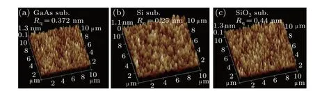
Fig. 2. Three-dimensional surface morphologies of (a) GaAs, (b) Si and(c)SiO2 after Ar-FAB treatment for 60 s.
3.2. Bonding strength and interface performance
3.2.1. Strength of GaAs/Si-based material bonding interfaces
The interfaces of the bonded GaAs/SiO2/Si and GaAs/Si wafer pairs are observed using SAM.The scanning results are shown in Figs. 3(a) and 3(b). The black areas represent areas with good bonding, while the white areas indicate the areas without bonding. Although it can be seen in Fig. 3 that the edge area is not bonded, the unbonded area is due to surface contaminants. There are a lot of contaminant particles on the edge of the wafer, which are mainly caused by the processes of atomic bombardment and wafer clamping. Particles are more likely to accumulate at the edge of the wafer. After the bonded wafer pairs are stored at RT for 24 h, the bonding energy is quantitatively measured by the blade-insertion method. A schematic diagram of the“crack-opening”method is shown in Fig. 4. The blade is inserted along the edge of the bonded pairs. The opening length is measured by SAM.The heterogeneous surface energy (γ) is calculated using the following equation:[26]
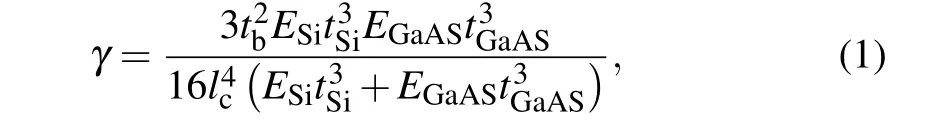
whereESiandEGaAsare the Young’s moduli for Si (1.30×10¹¹Pa)and GaAs(8.5×10¹⁰Pa),respectively,tSiandtGaAsare the thicknesses of the Si and GaAs wafers, successively,tbis the blade thickness (tb= 80 μm), andlcis the crack propagation length. The measured surface energies of the GaAs/SiO2/Si and GaAs/Si bonded pairs are 0.7 J/m2and 0.6 J/m2,respectively. In addition,the bonded pairs are fixed to a glass plate using paraffin wax, and the bonded pairs are then cut into small pieces 10×10 mm2in size by a chip cutting machine. The cutting surface is the GaAs side. A small piece is then taken out and fixed onto the glass plate again using paraffin wax. GaAs islets are cut to a size of 500×500 μm2and a depth of 725 μm from the small piece by the chip cutting machine. The GaAs islets are not detached, which indicates that the bonded pairs have high bonding quality.
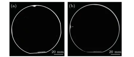
Fig. 3. (a) GaAs/SiO2/Si waferbonding pairs; (b) GaAs/Si waferbonding pairs.
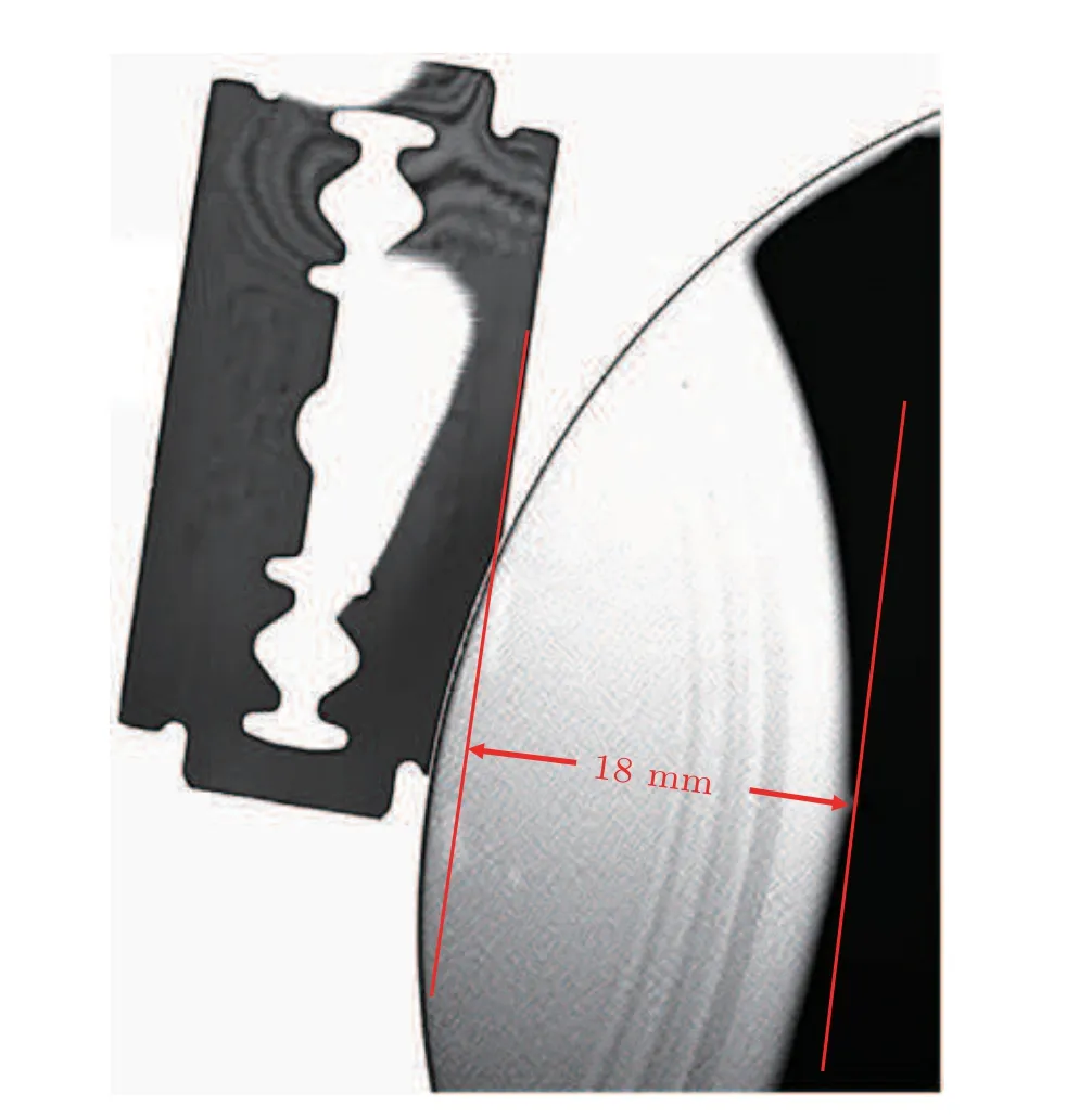
Fig.4. A schematic diagram of measuring the wafer bonding energy by the blade insertion method.
3.2.2. The 200 °C annealed GaAs/SiO2/Si bonding interface
In Fig. 5, STEM-HAADF images of the GaAs/SiO2/Si bonding interface are displayed. It can be seen from Fig.5(a)that a gap-free GaAs/SiO2/Si sandwich interface morphology is formed by the Ar atom activation treatment, and the thickness of the SiO2layer is about 300 nm. In Fig. 5(a), a small number of pollutant particles are attached to the SiO2layer,which is due to the need to deposit a carbon-powder protective layer on the surface before thinning. During the thinning process, carbon powder is attached to the interface. By capturing a high-resolution TEM image of the marked area in Fig.5(a),it can be seen that the interface is atomically bonded and free of structural damage, which confirms that the lower damage position is formed across the surface and the interface.As presented in Fig.5(b), there is an amorphous layer with a thickness of about 2 nm at the interface. On the left side of the amorphous layer,the GaAs lattice is damaged by Ar atom bombardment, resulting in an irregular lattice arrangement at the bonding interface. In order to further study the element composition at the interface,an element analysis for As,Ga,O and Si is conducted using EDX.The element distribution maps are shown in Figs.5(c)-5(f).It can be seen from Figs.5(c)and 5(d) that the As and Ga elements are diffused into the entire 2 nm-thick transition layer. In Figs. 5(e) and 5(f), some O and Si elements are distributed on the GaAs side. Because Si is harder than GaAs, when the bonding pairs are thinned by the FIB process, the Si material is above the GaAs material. Therefore, when the Si material is thinned first, a small portion of the Si and O elements are attached to the GaAs below. Figure 6 shows the percentage distributions of As,Ga,O and Si atoms across the bonding interface determined by EDX analysis. The horizontal and vertical axes represent the position of the bonding interface and the percentage of each atom,respectively. At a depth of 2 nm on the GaAs side of the bonding pair, the content of As is significantly higher than that of Ga.
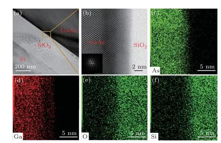
Fig. 5. (a), (b) Cross-sectional TEM images of the GaAs/SiO2/Si bonding interface after annealing at 200 °C. Element maps of As, Ga, O and Si are displayed in(c),(d),(e)and(f),respectively.
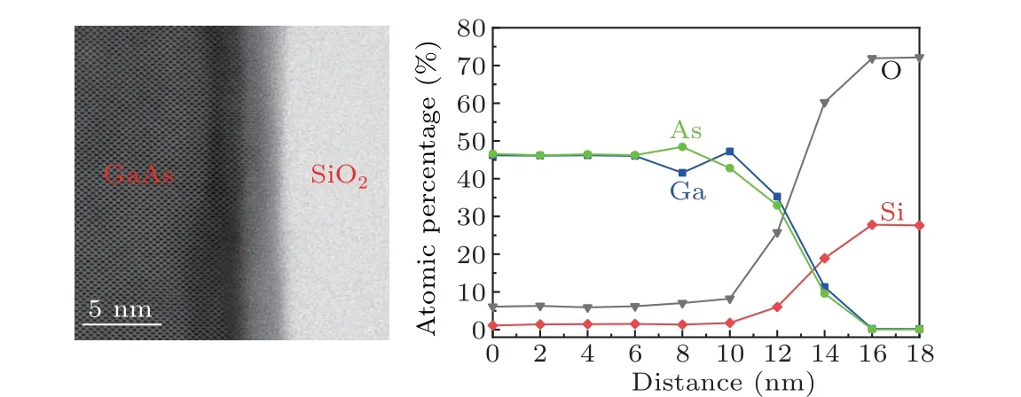
Fig. 6. Element analysis across the GaAs/SiO2/Si interface by EDX line scanning.
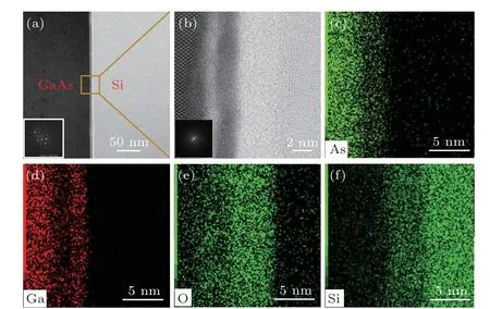
Fig.7.(a),(b)Cross-sectional TEM images of the GaAs/Si bonding interface after annealing at 200 °C.Element maps of As, Ga, O and Si are displayed in(c),(d),(e)and(f),respectively.
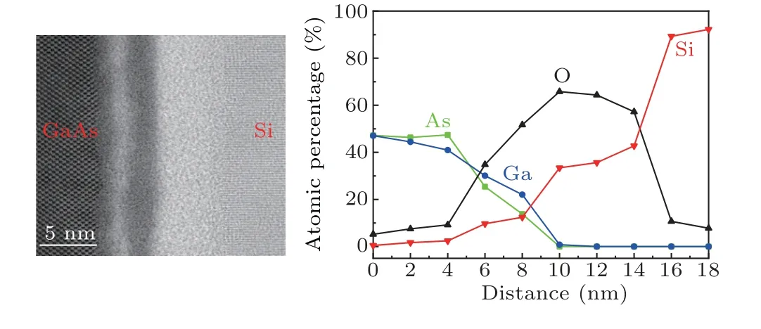
Fig.8. Element analysis across the GaAs/Si interface by EDX line scanning.
3.2.3. The 200°C annealed GaAs/Si bonding interface
Figure 7 shows a HAADF-STEM image of the GaAs/Si heterostructure interface after annealing at 200°C. By capturing a high-resolution TEM image from the marked area in Fig.7(a),it is observed that the interface is atomically bonded and free from structural damage. An amorphous layer with a thickness of about 7 nm is formed at the bonding interface,and the amorphous layer is relatively uniform, as shown in Fig.7(b). The amorphous layer at the interface is the result of activation treatment. The characteristic of Ar-FAB activation treatment is that two ultra-thin oxygen-rich layers are formed at the interface.Before activation,there is a natural oxide layer with a thickness of approximately 3-4 nm on the surfaces of both Si and GaAs substrates. Although the activation time is sufficiently long, only some of the natural oxides (such as Ga2O3or As2O3)can be removed. The element composition distribution of the bonding interface is revealed by EDX analysis in Figs.7(c)-7(f). It can be seen from the element distribution curve in Fig.8 that the intermediate amorphous layer is mainly composed of Ga,As,O and Si elements. The presence of oxides will inevitably interfere with current transmission at the GaAs/Si interface,thereby affecting the performance of solar cells.
3.3. Bonding mechanism
The influence of activation on GaAs/SiO2/Si and GaAs/Si bonded pairs can now be described,based on the observations and the analysis results.High-power atomic activation is likely to cause damage to the primary oxides of Si and GaAs, so it is deemed that there is a high degree of strain and reactivity on their surfaces. This may lead to a large amount of hydroxyl (GaAs-OH) on the surfaces of the GaAs and Si-OH groups.[27,28]Upon annealing, they can then polymerize in a similar fashion to that shown below:

A high number of interfacial covalent oxygen bridges are produced between the GaAs and the Si(GaAs-O-Si). In order to contain peeling stress during annealing and prevent debonding failures,a large number of interfacial GaAs-O-Si bridges is needed,especially in a very thermally mismatched bonding system. In addition, when the bonding surface is not sufficiently activated, the energy of most of the Ar atoms is too low to destroy and alter the surface chemistry of the Si and GaAs surfaces.Therefore,a smaller number of surface GaAs-OH and Si-OH groups appear,and lower H2O outward diffusion efficiency occurs,resulting in an ultimate decrease in the amount of GaAs-O-Si at the interface.[14]When the GaAs/Si wafer is not annealed, the diffusion of atoms such as Ga, As,O and Si at the interface is reduced. Due to the large amount of H2O that collects at the interface,it cannot diffuse into the Si and GaAs substrates. Therefore,the oxygen content at the interface increases,as shown in Fig.9.
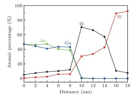
Fig. 9. Element analysis across the unannealed GaAs/Si interface by EDX line scanning.
Through reaction(2),strong covalent bonds are formed at the interface and play a leading role in robust bonding. After bonding, the bonded pairs are subjected to high-temperature annealing in a quartz furnace. High-temperature annealing accelerates the movement of water molecules produced by the reaction(2).Water molecules not only diffuse in the horizontal direction but also in the vertical direction. For GaAs/SiO2/Si and GaAs/Si bonded pairs, the water generated diffuses into the bulk Si through the oxide layer,and H2bubbles are formed at the interface,according to reaction[29]

The distribution of Ar atoms on the GaAs surface can be simulated by SRIM software,[30]and the density of the residual Ar atoms reaches a peak at a depth of 3 nm. The simulation also indicates that high-density vacancies are introduced at a depth of 2 nm.Quite a few point defects are produced by the interaction of fast Ar atoms with the GaAs surface. Sadanaet al.[31]confirmed that the displacement damage caused by atomic bombardment of GaAs can be dynamically annealed when the substrate temperature is higher than 100°C. The increase of temperature promotes the diffusion of defects,[32]which can eliminate the defects and prevent the formation of defect cascades. The element distribution curves of the interface obtained by EDX analysis in Figs.6 and 8 show that atomic intermixing occurs at the interface during bonding and subsequent annealing.
On the GaAs side of the bonded pairs,an amorphous layer is introduced,and lattice fringes can be observed,even in the vicinity of the interfaces, as shown in Fig. 6(a). Due to the introduction of point defects during the process of surface activation, transient diffusion is enhanced, as observed in implanted GaAs wafers. Vacancy agglomerates about 1 nm in size can be observed near the interfaces. Due to the formation of Frenkel-type defects on the As sites, the density ratio between the As and the Ga (As/Ga), is less than 1 down to a depth of 2 nm from the interface, and it is higher than 1 in the depth range from 2 nm to 6 nm. On the Si side of the wafer adjacent to the interface,an amorphous layer a few nm thick is formed. The density of various atoms at the interface changes gradually, resulting in a 4-8 nm-thick intermediate layer with a gradient composition. On the one hand,the layers are formed in such a way that the lattice mismatch between the interfaces of GaAs/SiO2/Si and GaAs/Si does not lead to highenergy and high-defect interfaces. This can reduce the elastic energy around the interfaces. On the other hand, a gradient layer can be formed due to the effect of roughness on the activated surface. In the bonding process,in order to maximize the chemical bond at the interface,atoms need to diffuse to fill the rough bonding interface. Through the surface activation process,the tough heterogeneous interface can be prepared at a low temperature. Therefore, the surface activation process not only needs to remove the surface oxide and produce the dangling bond, but also requires the enhancement of atomic diffusivity.
4. Conclusion
In this paper,GaAs/SiO2/Si and GaAs/Si heterointerfaces were fabricated by surface-activated bonding at room temperature. Cross-section scanning electron microscopy and dispersive x-ray spectroscopy (EDX) were used to confirm the presence of atomic intermixing at the bonding interface,which was mainly caused by the point defects introduced during the surface activation process. On the one hand,the point-defectassisted atomic diffusion can reduce the elastic energy around the heterogeneous interface. On the other hand, it can fill the rough bonding interface, so that tough heterogeneous interfaces between different materials can be prepared at room temperature. Therefore,the surface activation bonding conditions ought to be optimized to achieve bonding between different materials.
猜你喜歡
農(nóng)業(yè)科技與信息(2022年13期)2022-08-31 02:13:06
新疆藝術(shù)(2022年2期)2022-04-23 01:23:04
Chinese Physics B(2022年3期)2022-03-12 07:44:22
農(nóng)業(yè)科技與信息(2021年24期)2022-01-05 15:06:42
農(nóng)業(yè)科技與信息(2021年8期)2021-05-17 07:43:22
農(nóng)技服務(wù)(2020年5期)2020-06-12 01:39:32
應(yīng)用數(shù)學(xué)(2020年1期)2020-01-10 05:48:02
陶瓷科學(xué)與藝術(shù)(2019年10期)2019-12-18 05:36:42
甘肅農(nóng)業(yè)(2019年10期)2019-12-03 05:08:22
華人時(shí)刊(2017年15期)2017-10-16 01:22:23

- Chinese Physics B的其它文章
- Numerical simulations of partial elements excitation for hemispherical high-intensity focused ultrasound phased transducer*
- Magnetic-resonance image segmentation based on improved variable weight multi-resolution Markov random field in undecimated complex wavelet domain*
- Structure-based simulations complemented by conventional all-atom simulations to provide new insights into the folding dynamics of human telomeric G-quadruplex*
- Dual-wavelength ultraviolet photodetector based on vertical(Al,Ga)N nanowires and graphene*
- Phase-and spin-dependent manipulation of leakage of Majorana mode into double quantum dot*
- Deep-ultraviolet and visible dual-band photodetectors by integrating Chlorin e6 with Ga2O3