
Novel CMOS image sensor pixel to improve charge transfer speed and efficiency by overlapping gate and temporary storage diffusing node*
2021-01-21 02:08:48CuiYang楊翠GuoLiangPeng彭國(guó)良WeiMao毛維XueFengZheng鄭雪峰ChongWang王沖JinChengZhang張進(jìn)成andYueHao郝躍
Chinese Physics B 2021年1期
關(guān)鍵詞:雪峰
Cui Yang(楊翠), Guo-Liang Peng(彭國(guó)良), Wei Mao(毛維), Xue-Feng Zheng(鄭雪峰),Chong Wang(王沖), Jin-Cheng Zhang(張進(jìn)成), and Yue Hao(郝躍)
1School of Physics and Optoelectronic Engineering,Xidian University,Xi’an 710071,China
2Key Laboratory of Ministry of Education for Wide Band-Gap Semiconductor Materials and Devices,School of Microelectronics,Xidian University,Xi’an 710071,China
Keywords: CMOS image sensor,charge transfer efficiency,high-speed charge transfer,pinned photodiode
1. Introduction
Pinned photodiode(PPD)has been the most popular photoelectric detector in CCD and CMOS image sensors (CIS)due to the advantages of low noise, high quantum efficiency,and low dark current.[1]Up to now, several high-speed pixels based on the PPD technique have been proposed to meet the demand of the high-speed CIS applications.[2–5]For the high-speed pixels, the complete charge transfer with a limited transfer pulse is very difficult due to the limiting mechanism(thermal diffusion of the charges[6]),which means that the image lag will occur. Usually, a large dimension of photodiode is required in the high-speed pixels to improve the signal to noise ratio,[7]which will result in a longer charge transfer time (CTT).[8]Therefore, it is necessary to realize the fast charge transfer in the photodiode with proper approaches. Recently, a great deal of efforts have been made in this field and many effective methods have been proposed.By shaping PPDs, such as the horn shape,[3]a constant-field structure,[4]triangular shape,[4,9]bell-shaped photodiode,[9]trapezoidal shape,[10]or another grotesque photodiode,[5,11]the drift fields could be raised obviously compared with that in the rectangular photodiode. Besides,optimizing the doping profiles under the transfer gate(TG)of the 4-T pixels[12,13]is beneficial to improve the charge transfer speed. In addition,using one-step doping[7,14]or multi-step doping in the n-well of the photodiode[15–17]is proposed for creating the built-in drift fields in the photodiode. Moreover, the lateral electric field charge modulator[18]is proposed by means of MOS gateinduced lateral electric fields for enhancing the charge speed.Consequently, it could be concluded that the improvement of the lateral electrical fields could play a vital role in the enhancement of charge transfer speed in the photodiode.
In this paper,a novel CIS pixel(O-T pixel)with the highspeed charge transfer is presented and investigated. The study focus of this pixel is put on the further enhancement in the charge transfer speed with the same size of the photodiode as that of the conventional one. Compared with the conventional PPD pixel, the significant features of the proposed pixel are the overlapping gate(OG)and the temporary storage diffusing(TSD)region. Based on this, the charge transfer speed could be remarkably improved without any loss of the photodiode area. Two-dimensional numerical simulations with Sentaurus software are carried out to reveal the intrinsic operation mechanism of the proposed pixel by means of the electrostatic potential distributions and the transient operations. In addition,the relationship between the charge transfer time, the charge transfer efficiency, the photodiode length, and the OG length are studied systematically, aiming at the optimization of the minimized transfer time. These results are of great value for the design and further development of high-speed PPD pixels.
2. Device concept and characteristic
2.1. Device structures
Figures 1(a) and 1(b) show the schematic cross-sections of the conventional and the proposed PPD pixel structures,respectively.Xiis the length along X direction and Yiis the depth along Y direction of the different regions of the devices,whose main dimensions are given in Table 1.

Fig. 1. Schematic cross-sections of (a) the conventional structure and(b)the proposed structure. (c)Doping profiles of the conventional and the proposed pixels.

Table 1. Main structure specifications for the conventional and the proposed PPD pixels. X1 and X3 are discussed in this study.
A comparison of the architecture of the proposed pixel(O-T pixel) with the conventional PPD pixel shows that two parts are different. One is the long polysilicon gate, called overlapping gate (OG), stacking on the right side of the photodiode. The other is the lightly doped n-type region, called the temporary storage diffusing (TSD), existing between the OG and the transfer gate (TG). In addition, the TSD region is divided into two parts, which are labeled as part I and part II, respectively, as shown in Fig. 1(b). To clarify the specific device architectures, the doping profiles of the conventional and the proposed pixels are illustrated in Fig.1(c), where the sensed node (FD) between the TG and the reset gate (RST)is floated to enable that the signal charge can be extracted in TCAD simulations. The simulation conditions and the performance estimations will be shown in Section 3.
2.2. Overlapping gate for high-speed charge transfer
For the high-speed charge transfer, as mentioned above,the long overlapping gate is implemented in the proposed pixel to form the lateral electrical fields in the pinned photodiode,which is a popular method,e.g.,the reported high-speed applications.[2,14]
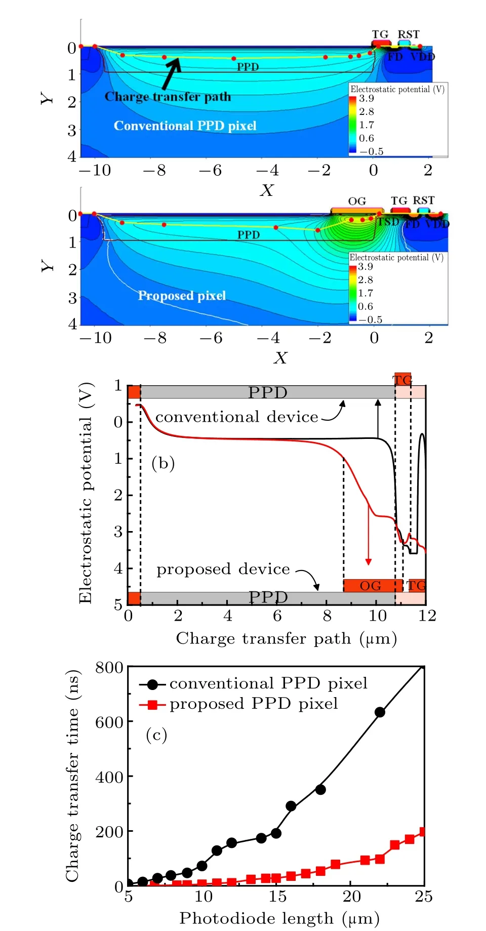
Fig. 2. Comparisons of the conventional and the proposed pixels, including(a)two-dimensional electrostatic potential distributions during charge transfer(namely,both OG and TG are in the on state),(b)onedimensional electrostatic potential distributions along the charge transfer path (namely, the yellow line with red dot in (a)). (c) The charge transfer time versus the various photodiode length(X1)for the conventional and the proposed pixels.
In order to exhibit the effect of the OG on the charge transfer speed,figure 2(a)illustrates the two-dimensional electrostatic potential distributions of the conventional and the proposed pixels during charge transfer(namely,both OG and TG are in the on state). In addition, the one-dimensional electrostatic potential distributions along the charge transfer path(namely, the yellow line with red dot in Fig.2(a))are plotted in Fig.2(b). It can be observed that,due to the long OG stacking above the PPD,the potential difference in the photodiode of the proposed device is greater than that in the conventional counterpart,which demonstrates the stronger electric fields in the photodiode and thus the high-speed charge transfer during charge transfer in the proposed device. In Fig.2(c),the charge transfer time as a function of the photodiode length(X1)for the conventional and the proposed pixels is depicted. Obviously,the charge transfer speed of the proposed pixel is faster than that of the conventional pixel, which proves that the overlapping gate can improve the charge transfer speed significantly.
2.3. Temporary storage diffusing node for suppressing charge spillback
Indeed, the overlapping gate can enhance the charge transfer speed in the photodiode, as discussed above. However, the long overlapping gate, which is a big MOS capacitance, can retain some carriers in the inversion channel when the OG is switched on.As the OG transitions from high to low,the carriers in the OG channel are likely to return to the photodiode, this phenomenon is called charge spillback. To suppress the charge spillback, the TSD concept is implemented in the proposed pixel (O-T pixel), where the TSD region has two parts, as depicted in Fig.1(b). Part I is the lightly doped n-type region for forming the electrostatic potential step under the OG to drive the carriers from the OG channel to the TSD.Besides,part II is an n-type region,whose doping dose is heavier than that of part I,for collecting the carriers of part I as the OG bias(VOG)is low enough.
Figure 3 presents the proposed doping process for fabricating the TSD node with two layouts (mask-1 and mask-2).Firstly, by using mask-1, boron ions implantation is implemented to form a p-type region, which is shown in Fig. 3(a).This p-type region is used to isolate the PPD, the TSD, and the FD from each other. Moreover, it is also used as the half transfer gate threshold voltage adjustment. Secondly,by using mask-2,arsenic ions implantation is implemented to form part I of the TSD,which is illustrated in Fig.3(b). Finally,by using mask-2, arsenic ions implantation is carried out after the polysilicon gate process to form part II of the TSD, which is depicted in Fig.3(c).
To clarify the suppression of the charge spillback by means of the proposed doping process,the comparison analyses of the conventional PPD pixel,the proposed pixel without the TSD,and the proposed pixel with the TSD are performed,as shown in Fig.4. Figure 4(a)shows the structure difference among the three pixels. In addition, in Fig. 4(b), the corresponding two-dimensional electrostatic potential distributions are depicted,in which the charge transfer paths are also illustrated by the yellow line with red dot. Figure 4(c) illustrates the one-dimensional electrostatic potential distributions along the charge transfer paths, which are extracted from Fig. 4(b).It could be observed that the potential difference along the charge transfer path in the proposed devices with or without the TSD is greater than that in the conventional one,which indicates the higher charge speed and charge transfer efficiency in the proposed pixel compared with the conventional counterpart,as shown in Fig.4(d).
Careful observations on Fig. 4(c) show that there exists a potential barrier near the right side of the photodiode in the proposed pixel without the TSD compared with the proposed pixel with the TSD. This barrier will prevent the carriers in the PPD from moving into the sensed node(FD)to some extent. Thus, the proposed pixel with the TSD has a higher charge transfer efficiency(CTE),compared with the one without the TSD, as shown in Fig. 4(d). In addition, compared with others,the proposed pixel with the TSD shows the shortest charge transfer time to approach the highest CTE, which further demonstrates the high charge transfer speed.

Fig.4. Comparison of the three pixels,including(a)two-dimensional doping profiles,(b)electrostatic potential profiles,(c)one-dimensional electrostatic potential profiles extracted from(b),and(d)charge transfer efficiency versus various charge transfer time.
2.4. Analyses of the suppression of charge spillback in the proposed device
To analyze the capacity of the suppression of charge spillback in the proposed device,figure 5(a)shows the electrostatic potential profiles along the charge transfer path under five conditions(namely,A,B,C,D,and E conditions). From A condition to E condition(namely,VOGvaries from 2.8 V to-0.5 V,and VTGvaries from 3.3 V to -0.5 V), it could be seen that the potential difference in the PPD is reduced gradually with the decreasing VOG,which means that the charge transfer will be weaken gradually. Especially, under D and E conditions,the charge transfer in the photodiode is stopped due to the OG switched off.
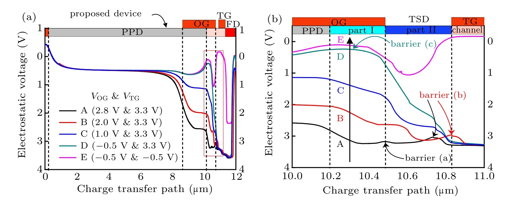
Fig.5. (a)Electrostatic potential profiles along the charge transfer path in the proposed pixel under five conditions(namely,A condition to E condition). (b)Zoomed-in view of the red rectangle region in(a)for highlighting the charge transfer in the TSD region.
The detailed analyses are illustrated in Fig.5(b)by means of the zoomed-in view of the red rectangle region in Fig.5(a).As shown in Fig. 5(a), the maximum potential difference in the PPD appears under A condition (VOGis 2.8 V, and VTGis 3.3 V),which could reach the highest charge transfer speed.And in Fig.5(b),there would be some carriers left in part I and part II because of the existence of barrier (a) and barrier (b).Under B condition(VOGis 2.0 V,and VTGis 3.3 V),the barrier(a) between part I and part II is removed compared with the case under A condition, and the electrostatic potential in part II is greater than that in part I,which means that the carriers in part I can be transferred into part II.Then,under C condition(VOGis 1.0 V, and VTGis 3.3 V), the potentials in parts I and II become lower so that the barrier(b)between part II and the TG channel under B condition is eliminated,and thus the carriers in part II can move into the sensed node(FD)through the TG channel. Next,under D condition(VOGis-0.5 V,and VTGis 3.3 V),barrier(c)is formed in part I as the OG is turned off,and barrier (c) could prevent the carriers from flowing back to the PPD. Finally, under E condition (VOGis -0.5 V, and VTGis -0.5 V), the TG is switched off and thus the sensed node (FD) is isolated for reading out the voltage signal. The analyses above demonstrate that it is difficult for the carriers to return to the photodiode in the proposed pixel after charge transfer,which proves the effective suppression of the charge spillback in the proposed device.
3. Performance estimation
3.1. Simulation condition
In TCAD simulations,the main physics models are used in Sentaurus tools, including mobility (doping dependence high field saturation),effective intrinsic density(band gap narrowing(old slot boom)),recombination(SRH(doping dependence)Auger).Furthermore,the main solving models are coupled {Poisson electron hole}. In addition, the temperature is 300 K and the optical generation module with the monochromatic source (the wavelength is 0.9 μm and the intensity is 1.0 W/cm2) based on the time-dependence function is used for carriers generation in the transient simulations. Note that 1.0 μm device width(i.e.,along the direction looking into the cross section)is used in TCAD simulations with 110 nm CIS process conditions.
3.2. Estimation for charge transfer efficiency and time
For quantization of the proposed device, for instance, a proposed device with 10 μm long photodiode and 1.5 μm long OG will be estimated by means of TCAD in this section. Figure 6(a)illustrates the timing diagram of the proposed device,which has three parts (i.e., resetting PPD, accumulation, and charge transfer). During resetting PPD, the RST is biased at 3.3 V for 50 ns and then the sensed node is reset to about 2.6 V.Afterwards,the OG is biased at 2.8 V for 19 ns and the TG is biased at 3.3 V for 20 ns in order to reset the photodiode. The transfer gate pulse is one nanosecond longer than the overlapping gate pulse in order to transfer the rest of carriers in the TSD to the sensed node. During accumulation,a monochromatic light source(i.e., the wavelength is 0.9 μm and the intensity is 1.0 W/cm2) is switched on for 10 ns to obtain the photo-generated carriers. During photo-generated electrons transfer from the photodiode to the sensed node,the voltage pulses of the OG,the TG,and the RST are the same to those of the first part of the timing diagram(resetting PPD).
Figures 6(b)and 6(c)present the transient simulation results. Note that it is assumed that the PPD is fully depleted if only one electron is left in the photodiode.From the partial enlarged drawing in Fig.5(b),it can be observed that the charge transfer time is about 5.779 ns, thus the total charge transfer time is about 6.779 ns because the TG pulse is one nanosecond longer than the OG pulse. Figure 6(b)shows that the electron number in the photodiode(QPPD-Sig)is about 1292.6e. Moreover,the charge number approaches zero in the photodiode after the charge transfer,which means that there is no signal lag.Likewise,as shown in Fig.6(c),the charge numbers in the FD before and after the charge transfer are about 7621526.1e and 7622818.6e,respectively. Thus,the sensed node has collected 1292.5e(QFD-Sig)after the exposure phase.
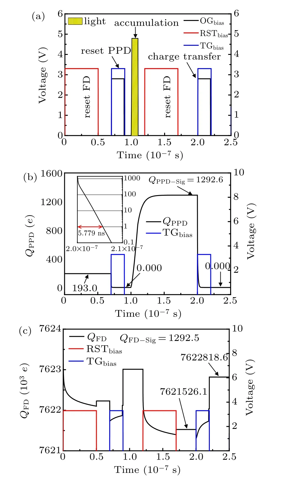
Fig. 6. The operation and transient results of the proposed pixel. (a)Timing diagram of the proposed pixel operation. (b) Charge number in the photodiode varying with time. (c)Charge number in the sensed node versus time.
Usually, the charge transfer efficiency (CTE) is used to evaluate the image lag.[3]It is defined as
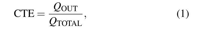
where QOUTis the number of the signal charges that are transferred from the photodiode into the sensed node,and QTOTALis the number of the initial charges that are generated in the photodiode after illumination. From the simulation results,QTOTALis QPPD-Sig,1292.6e,and QOUTis QFD-Sig,1292.5e.As a result, the CTE is about 99.99%. It is obvious that the CTE approaches 100%,i.e.,complete charge transfer.
4. Device optimization
4.1. Optimization of TSD doping process
Signal lag arises from the incomplete charge transfer.[3]In the proposed pixel, the temporary-storage-diffusing node(TSD)has an influence on the charge transfer,as discussed in Subsection 2.3. To optimize the TSD region,the influences of the doping dose of part I and part II on the electrostatic potential profiles along the charge transfer path are discussed in this section.
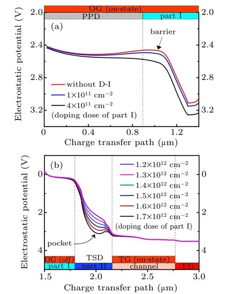
Fig. 7. (a) Influence of the doping dose of part I on the electrostatic potential profiles along the charge transfer path under A condition of Subsection 2.4. (b)Influence of the doping dose of part II on the potential profiles along the charge transfer path under D condition of Subsection 2.4.
From Fig. 7(a), it can be found that with the increasing doping dose of part I, the potential barrier height in part I is decreasing under A condition of Subsection 2.4. When the doping dose of part I is 4 ×1011cm-2, the potential barrier is removed thoroughly, which means that all carriers can be transferred from the PPD to part I. Figure 7(b) shows the influence of the doping dose of part II on the electrostatic potential profiles from the TSD to the FD.It can be seen that the potential pocket depth in part II is directly proportional to the doping dose of part II partly. When the doping dose of part II is set to less than 1.5×1012cm-2, the potential pocket can be eliminated. Therefore,if the doping dose of part II is small enough,the carriers can be completely transferred from part II to the FD under D condition of Subsection 2.4.
As a result, it can be concluded that the proposed pixel with the proper TSD doping enables all carriers to be completely transferred from the photodiode to the sensed node,which means no signal lag.
4.2. Optimization of overlapping gate length for minimum charge transfer time
Charge transfer in the photodiode is driven by the lateral electric fields that are formed by the overlapping gate in the proposed pixel,as discussed in Subsection 2.2. Therefore,the OG length has an effect on the charge transfer speed of the proposed pixel. Figure 8 shows that charge transfer time as a function of the OG overlapping length in the proposed pixel with a 10 μm long photodiode. According to the results, the transfer time has a minimum value, 4.862 ns, and the corresponding OG overlapping length(X3)is 1.92 μm. In addition,it can be observed that the OG length hardly affects the charge transfer efficiency of the proposed pixel.
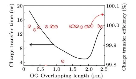
Fig.8. Charge transfer time versus the OG overlapping length(X3)and the corresponding charge transfer efficiency.
5. Conclusion
A novel CMOS image sensor pixel with the overlapping gate and the temporary-storage-diffusing node has been presented in this paper, with emphasis on the high-speed charge transfer. Systematical analyses of the charge transfer performance, the device physical mechanisms, and the device optimization designs are performed. Simulations exhibit that the obvious reduction in the charge transfer time compared with the same photodiode size of the conventional PPD pixel could be realized by optimizing the overlapping gate in the proposed pixel. These results demonstrate the advantages of the proposed pixel in high-speed CIS.
猜你喜歡
奧秘(2023年3期)2023-05-30 04:58:26
Chinese Physics B(2021年1期)2021-01-21 02:07:22
少兒科技(2021年10期)2021-01-20 23:19:26
雜文月刊(2019年19期)2019-12-04 07:48:34
西部論叢(2017年8期)2017-12-01 01:10:14
試題與研究·教學(xué)論壇(2017年6期)2017-02-28 05:41:10
中國(guó)三峽(2016年5期)2017-01-15 13:58:43
高中生·天天向上(2016年2期)2016-04-06 04:47:00
歌海(2016年1期)2016-03-28 10:08:55
現(xiàn)代企業(yè)文化(2015年1期)2015-02-28 18:58:45
- Chinese Physics B的其它文章
- Numerical simulation on ionic wind in circular channels*
- Interaction properties of solitons for a couple of nonlinear evolution equations
- Enhancement of multiatom non-classical correlations and quantum state transfer in atom–cavity–fiber system*
- Protein–protein docking with interface residue restraints*
- Effect of interaction between loop bases and ions on stability of G-quadruplex DNA*
- Retrieval of multiple scattering contrast from x-ray analyzer-based imaging*