
Enhanced mobility of MoS2 field-effect transistors by combining defect passivation with dielectric-screening effect*
2021-01-21 02:15:26ZhaoLi李釗JingPingXu徐靜平LuLiu劉璐andXinYuanZhao趙心愿
Chinese Physics B 2021年1期
Zhao Li(李釗), Jing-Ping Xu(徐靜平), Lu Liu(劉璐), and Xin-Yuan Zhao(趙心愿)
School of Optical and Electronic Information,Huazhong University of Science and Technology,Wuhan 430074,China
Keywords: MoS2 transistor,sulfur vacancy,high-k dielectric,mobility
1. Introduction
Since the first discovery of graphene in 2004, twodimensional(2D)materials have been intensively investigated due to their unique structural characteristics and excellent electrical properties.[1–3]Although graphene has been shown to have extremely high carrier mobility,the lack of its bandgap limits its application in logic devices. Unlike graphene,MoS2has an appropriate bandgap and is one of the most representative 2D semiconductor materials in transition metal dichalcogenides(TMDs). It has been found that the bulk MoS2shows an indirect bandgap of 1.2 eV and the monolayer MoS2exhibits a direct bandgap of 1.8 eV,[4–6]which has a wide range of applications in field-effect transistors, memories,[7,8]logic circuits,[9,10]photodetectors,[11]etc.
Theoretical calculations based on the density functional theory demonstrated that the mobility of the monolayer MoS2can reach 410 cm2/V·s at room temperature.[12,13]However,experimentally,the mobility of the monolayer MoS2as channel material of the field-effect transistor (FET) is still far from its intrinsic limit, which is originated from the effects of some factors, e.g., charged impurities,[14,15]surface defects,[16]phonon scattering,[17]etc.The high-dielectric constant (k) gate dielectrics were widely used to reduce the influence of the charged impurities and can effectively screen their Coulomb scattering, which has been confirmed in many experiments.[6,14,18]Li et al.[19]fabricated MoS2FET with a back-gate structure on Si substrate with high-k Al2O3as the gate dielectric,and its mobility has been significantly improved as compared with the gate dielectric of SiO2. On the other hand,the defect engineering is one of the effective ways to further improve the performance of MoS2devices. Yu et al.[12]found that the sulfur vacancies,which are the main type of intrinsic defects in MoS2, can be effectively repaired by(3-mercaptopropyl)trimethoxysilane(MPS)under a mild annealing, resulting in a significant reduction of the Coulomb impurity and short-range scatterings. However, these investigations usually focused on one of the influencing factors and rarely combined two or more factors for a comprehensive analysis. Therefore, in this work, we adopt a facile approach to combine the defect engineering with the dielectric-screening engineering to fabricate the back-gated MoS2transistors to investigate the effects of the surface passivation of MoS2and the high-k gate dielectrics on electrical characteristics of devices,especially on the carrier mobility.
2. Experiment s
The device fabrication begins with thermally-growing SiO2on the cleaned heavily-doped p++-Si wafers with a resistivity of 0.01 Ω·cm,and the thickness of the SiO2was measured to be 32 nm by an ellipsometer. The few-layered MoS2flakes were obtained by a micromechanical exfoliation of the bulk MoS2crystal purchased from SPI,[20]and then transferred to the SiO2/p++-Si substrates with the help of Scotch tape. The thickness of these MoS2flakes can be roughly distinguished by their colors:[21]gray, blue, and purple correspond to the bulk,multilayer,and few-layered MoS2,respectively, as shown in Fig. 1(a). Figure 1(b) shows the AFM height image of the few-layered MoS2flake with a thicknesses of 5.32 nm (~8 layers). The few-layered MoS2flake was chosen to fabricate transistors because it has higher density of states than the monolayer MoS2, which will result in a rather high drive current.[22,23]
Then, these MoS2flakes were vulcanized in a tube furnace. The one gram of sulfur powder was placed downstream in constant-temperature zone and the MoS2/SiO2/p++-Si substrates were placed upstream ~10 cm away from the sulfur powder in the same temperature zone,as shown schematically in Fig.1(c).During the vulcanization,the furnace temperature was hold at 200?C(an optimum temperature via experiments)for one hour, and the diffusion rate of the sulfur vapor was controlled by adjusting the flow rate of the carrier gas(N2).
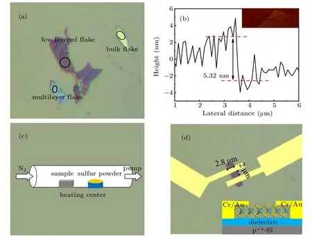
Fig.1. (a)Optical micrographs of different-thickness MoS2 flakes on the dielectric; (b)the AFM height image of the few-layered MoS2 flake; (c) schematic diagram for sulfur treatment on MoS2 flakes; (d) optical micrographs of MoS2 transistor with the inset showing its cross-section diagram.
Next, the sulfur-treated MoS2flakes were used to fabricate the back-gated FETs. Electron beam lithography was used to pattern the source/drain(S/D)of MoS2transistors,and 15-nm Cr/45-nm Au were successively deposited by electronbeam evaporation,followed by a liftoff processing to form S/D electrodes, as shown in Fig. 1(d). The channel length (L) of all transistors was 2 μm and the channel width (W) was 1–4 μm depending on the shapes of the MoS2flakes, and the schematic diagram of the transistor structure is shown in the inset of Fig. 1(d). Lastly, the transistors were rapidly annealed at 300?C for 300 s in a N2atmosphere (1500 sccm)with a pressure of 0.2 Torr to reduce the contact resistance between the MoS2and the Cr/Au electrodes.[24]For comparison, a transistor with the MoS2unexperienced vulcanization was also fabricated as a control sample. Electrical measurements of the transistors were performed using a Keithley 4200-SCS semiconductor parameter analyzer under a light-tight and electrically-shielded condition at room temperature.
3. Results and discussion
To ensure the validity of the measured results, at least four transistors for each sample were measured. Figure 2(a)shows the typical drain current (Id) versus drain–source voltage(Vds)curves of the transistors with and without the MoS2treated by vulcanization. It can be clearly seen that the transistors have good output characteristics with clear cut-off region, transition region, and saturation region. Obviously, the post-vulcanization transistor has higher on-state current than the pre-vulcanization transistor,attributing to the reduction of the sulfur defects during vulcanization of MoS2. Figure 2(b)is the Id–Vdscurves in the linear region (Vdsfrom -0.1 V to 0.1 V), and a good linear relationship between Idand Vdscan be observed,indicating a good ohmic contact between the MoS2and the Cr/Au electrodes. Figures 2(c)and 2(d)are the transfer characteristics of the MoS2FETs with Vds=0.2 V in linear scale and in semi-log scale, respectively, and the drain current is normalized to eliminate the effect of different channel widths on the output current. The threshold voltage (Vth)is extracted by the linear extrapolation method through the maximum-slope point of the Id–Vdscurve in Fig. 2(c) to be 1.39 V and 2.43 V before and after vulcanization,respectively.The positive shift of Vthafter the sulfur treatment is mainly due to the reduction of the sulfur vacancies in the MoS2flakes.[25]

Fig. 2. (a) Output characteristics of MoS2 FETs with and without sulfur treatment; (b) Id–Vds curves in the linear region of the back-gated MoS2 transistor with MoS2 treated by vulcanization;transfer characteristics with Vds=0.2 V in linear scale(c)and in semi-log scale(d);(e)extracted mobility from the transfer curves in(c);(f)PL spectrum of MoS2 flakes before and after vulcanization.
From the transfer curves of the two transistors before and after vulcanization,their field-effect mobility can be extracted using by
where Coxis the oxide capacitance per unit area (1.08×10⁻⁷F/cm2for 32-nm thick SiO2), L and W are the channel length and width, respectively, and Vgsis the gate–source voltage. As can be seen from Fig. 2(e), the mobility of the transistor with sulfur treatment on MoS2is largely enhanced as compared to that of the non-treated MoS2transistor (46.03 cm2/V·s vs. 25.71 cm2/·V·s). Obviously, this is attributed to the reduction of the sulfur-vacancy defects in MoS2by the sulfur treatment,because these defects could act as scattering centers to slow down the carrier transportation in the channel, resulting in low mobility. This can be supported by Raman spectral analysis,because the measured photoluminescence(PL)intensity depends on the surface defect density of MoS2and the PL intensity weakens as the surface defects decrease.[26]Clearly, from Fig. 2(f), the PL intensity of the MoS2flakes becomes weaker after the sulfur treatment compared to that before the sulfur treatment,indicating the reduction of the defects related to the sulfur vacancies. In addition,the peak of the MoS2PL intensity is at 1.78 eV,which is consistent with the forbidden band of the few-layered MoS2.AFM was employed to analyze the surface morphology of the MoS2flakes before and after vulcanization. It was observed that the surface roughness was decreased by ~0.09 nm after the vulcanization,further indicating the role of the vulcanization. From the above analyses, it can be concluded that the sulfur treatment on MoS2can enhance the carrier mobility in the channel due to the reduction of the surface roughness and the defects in the MoS2flakes.
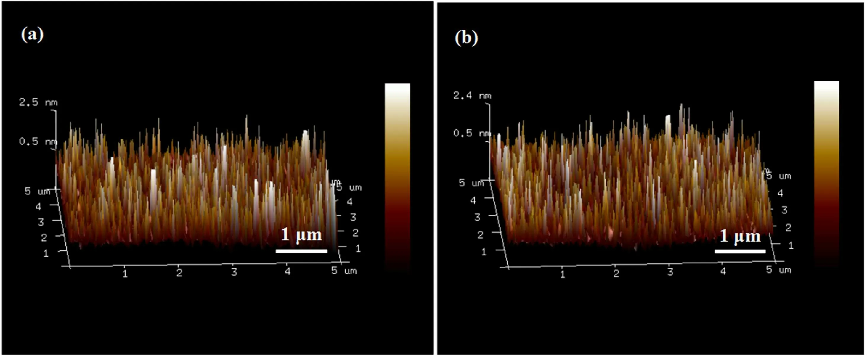
Fig.3. AFM surface images(5×5 μm2)of MoS2 flakes before(a)and after(b)sulfur treatment.
High-k materials,e.g.,hafnium dioxide(HfO2),alumina(Al2O3),are widely used in CMOS devices and play an important role as gate dielectrics in MoS2-based transistors, since they are expected to screen the charged-impurity scattering near the channel, resulting in an enhancement of the carrier mobility.[19,27,28]For this purpose,high-k Al2O3and HfO2are employed to replace SiO2as the gate dielectric of the MoS2transistors respectively to further improve the carrier mobility.The Al2O3and HfO2thin films were grown by atomic layer deposition(ALD)at 200?C with TDMA-Hf(Hf(N(CH3)2)4),TMA (Al(CH3)3), and H2O as Hf, Al, and O precursors, respectively, and N2as the carrier/purge gas. The injection schedule for one cycle of Al2O3and HfO2deposition was 0.02 s–15 s–0.015 s–15 s of TMA–N2–H2O–N2and 0.15 s–15 s–0.015 s–15 s of TDMA–Hf–N2–H2O–N2, respectively.The Al2O3and HfO2thin films with a thickness of 32 nm were obtained after 291 and 311 deposition cycles, respectively. The metal/Al2O3or HfO2/Si MOS capacitors with an area of 7.85×10⁻⁵cm2were fabricated using gold as the gate electrode to characterize the dielectric properties of the two films.
Figure 4 shows the typical high-frequency (1 MHz) C–V curves for the metal/HfO2/p++-Si and metal/Al2O3/p++-Si MOS capacitors. The accumulation (or oxide) capacitances of the HfO2and Al2O3MOS capacitors are 37 pF and 27 pF,respectively. According to the formula k = (Coxtox)/(Aε0),where ε0is the vacuum permittivity, A is the electrode area,and toxis the physical thickness of the HfO2or Al2O3, the equivalent k-value of the gate dielectric is extracted to be 11.51 and 6.91 for the HfO2and Al2O3gate dielectrics,respectively.Correspondingly,the calculated capacitance-equivalent thickness (CET=(εox/k)tox, εoxis the relative dielectric constant of SiO2) of the HfO2dielectric is smaller than that of the Al2O3dielectric(10.84 nm vs. 18.06 nm),which is beneficial for enhancing the dielectric-screening effect and scaling down the MoS2-based transistor. Even so, the k-value of Al2O3is more suitable for balancing the charged-impurity scattering and the phonon scattering on electrons in the MoS2channel,because the high-k dielectrics can reduce the Coulomb scattering through the dielectric-screening effect but simultaneously can also cause a serious phonon scattering.[17]Moreover, as can be seen from Fig.4,the C–V hysteresis of the Al2O3sample is much smaller than that of the HfO2sample, implying the fewer defect states in the former than the latter.
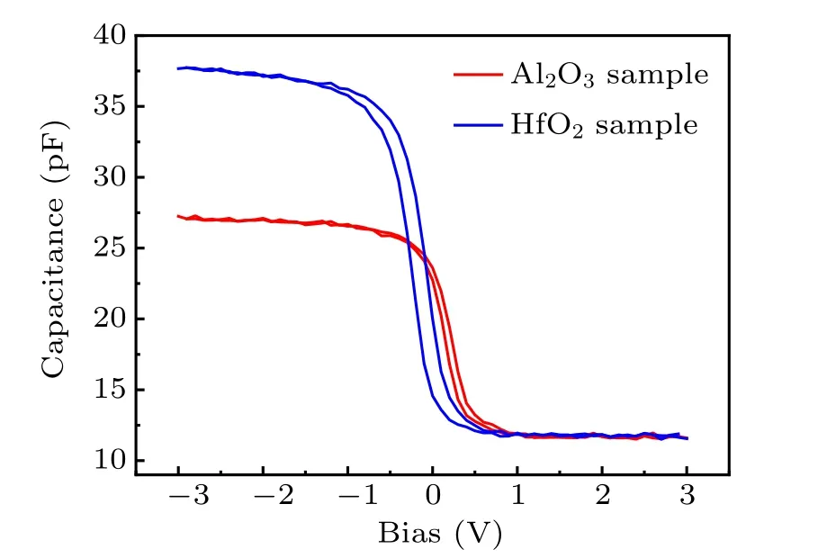
Fig.4. The C–V curves of metal/Al2O3/p++-Si and metal/HfO2/p++-Si MOS capacitors.
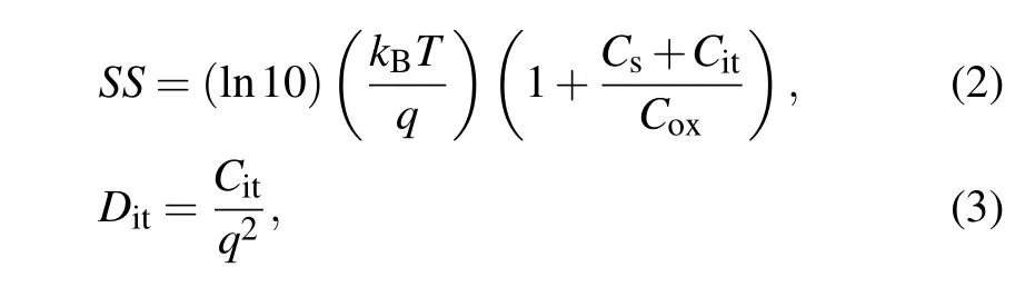
Figures 5(a) and 5(b) show the typical transfer characteristics of the MoS2transistors with different gate dielectrics before and after the sulfur treatment on MoS2, respectively,and the corresponding changes of their mobility with Vgsare depicted in Figs. 5(c) and 5(d). The extracted on/off current ratio,peak mobility(μ),and subthreshold swing(SS)for these transistors are listed in Table 1. It can be seen that the transistors with different gate dielectrics (SiO2, Al2O3, and HfO2)have a similar on/off current ratio before the MoS2vulcanization. After the sulfur treatment on MoS2, the on/off current ratios of the transistors are increased, with the maximum obtained in the transistor with Al2O3gate dielectric(2.11×10⁶).
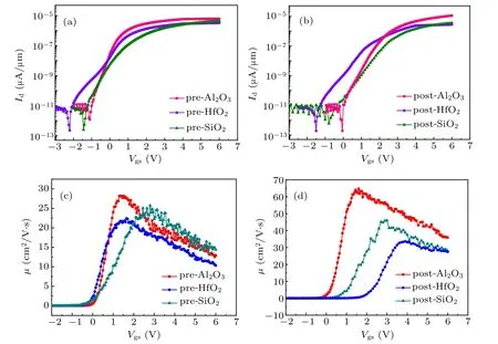
Fig.5. Typical transfer characteristics of MoS2 transistors with different gate dielectrics(a)before and(b)after sulfur treatment on MoS2;the extracted mobility of MoS2 transistors with different gate dielectrics(c)before and(d)after sulfur treatment on MoS2.
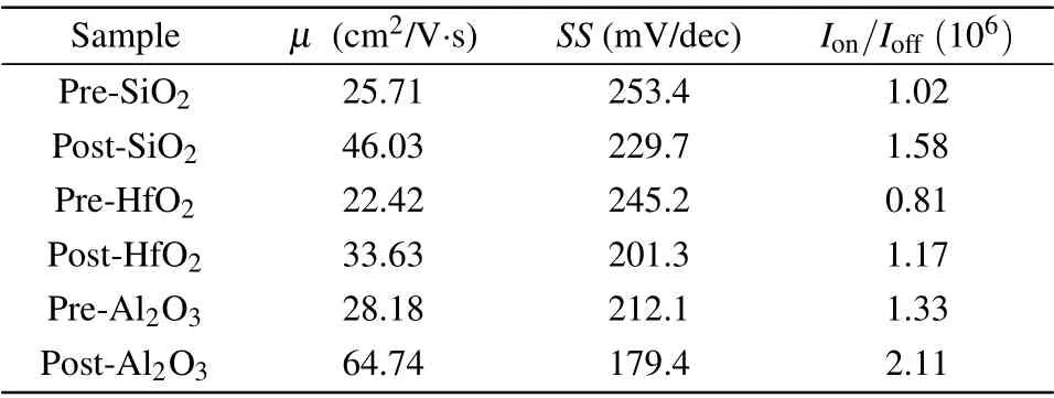
Table 1. Electrical properties of the MoS2 FETs with SiO2, HfO2, and Al2O3 as the gate dielectric respectively before and after the sulfur treatment.
The extracted SS’s for the transistors with SiO2, HfO2, and Al2O3gate dielectrics are 253.4 mV/dec, 245.2 mV/dec, and 212.1 mV/dec before the sulfur treatment on MoS2and become 229.7 mV/dec, 201.3 mV/dec, and 179.4 mV/dec, respectively, after the sulfur treatment on MoS2, i.e., the SS is significantly lowered after the MoS2vulcanization as compared with that before the vulcanization, with the minimum obtained in the transistor with Al2O3gate dielectric.The small SS implies a good interface quality between MoS2and Al2O3because the SS is related to the interface-state density(Dit)
where Csis the barrier capacitance per unit area at the MoS2surface and can be ignored because the SS is generally extracted in the deep subthreshold region; Citis the interfacestate capacitance per unit area; kBis the Boltzmann constant,and q is the electronic charge. According to Eqs. (2) and(3), the calculated interface-state density between MoS2and Al2O3is 3.50×10¹²eV-1·cm-2before the sulfur treatment and 2.75×10¹²eV-1·cm-2after the treatment.
The mobility of the MoS2transistor is a main concern.The extracted peak mobility for the transistors with SiO2,HfO2,and Al2O3as the gate dielectric and the sulfur treatment on MoS2is 46.03 cm2/V·s,33.63 cm2/V·s,and 64.74 cm2V·s,respectively, which is significantly improved as compared to their counterparts without the sulfur treatment on MoS2(1.5–2.3 times). The high-k oxides are usually used as the gate dielectrics to suppress the Coulomb scattering owing to their dielectric-screening effect.Therefore,the significant improvement for the transistor with Al2O3as the gate dielectric can be attributed to the dielectric-screening effect. However, an opposite trend is observed for the MoS2transistor with HfO2as the gate dielectric, which has an even lower mobility than its counterpart with SiO2as the gate dielectric. Ma et al.[17]reported this similar phenomenon and argued that although the high-k dielectrics can reduce the Coulomb scattering by their dielectric-screening effect at room temperature, an enhanced surface-phonon scattering produced by them counteracts this advantage. When the phonon scattering is negligible,the carrier mobility is almost limited by the Coulomb scattering and is enhanced as the k-value of the gate dielectric increases.However, when the k-value is too large, the electrons in the channel are more likely to excite the phonons in the surrounding dielectric through the remote Coulomb interactions,so that the channel carriers are more strongly affected by the phonon scattering,resulting in the reduction of the mobility. Based on the explanation, the MoS2transistors with Al2O3and HfO2as the gate dielectric exhibit the enhanced and reduced mobility, respectively, as compared with their counterpart with SiO2as the gate dielectric, because the former has a suitable k-value so that the dielectric-screening effect is dominant,and the latter has a larger k-value so that the phonon scattering overwhelms the dielectric-screening effect. The same phenomenon was also demonstrated in Konar’s research on the effect of the high-k gate dielectric on the charge transport in the graphene FETs.[29]
4. Conclusion
In summary, the sulfur-treated few-layered MoS2backgated FETs with different gate dielectrics have been fabricated and their electrical properties are compared. It is found that the transistors with the sulfur treatment on MoS2channel exhibit a greatly enhanced carrier mobility as compared to their counterparts without the sulfur treatment. This is mainly owing to the reduction of the defects related to the sulfur vacancies during the vulcanization of the MoS2. Further, it is found that when the high-k Al2O3and HfO2are used to replace SiO2as the gate dielectric, the mobility of the relevant transistors gets enhanced and reduced, respectively. The involved mechanisms lie in that a suitable k-value of the former leads to an effective dielectric-screening effect and a larger kvalue of the latter induces an enhanced phonon scattering over the dielectric-screening effect. For the Al2O3-gate dielectric MoS2FET,its carrier mobility is tripled after the sulfur treatment on MoS2(64.74 cm2/V·s) as compared to that before the sulfur treatment, and also its on/off current ratio and subthreshold swing are improved. Therefore,the sulfur treatment on MoS2provides a facile solution to improve the mobility of the MoS2FETs,especially for the transistor with a reasonable k-value gate dielectric,e.g.,Al2O3.
猜你喜歡
小學生學習指導·中年級(2024年4期)2024-06-06 16:05:21
小學生學習指導·中年級(2024年3期)2024-04-21 03:11:28
小學生學習指導·中年級(2024年2期)2024-02-25 02:10:49
蘭州文理學院學報(自然科學版)(2023年6期)2023-11-24 11:09:14
音樂教育與創(chuàng)作(2022年8期)2022-10-11 04:07:58
蘭州文理學院學報(自然科學版)(2022年4期)2022-07-12 01:48:12
青年文學家(2022年5期)2022-03-25 13:17:27
心聲歌刊(2020年3期)2020-08-12 09:37:26
基層中醫(yī)藥(2020年2期)2020-07-27 02:45:54
音樂天地(音樂創(chuàng)作版)(2019年12期)2019-12-09 00:23:01
- Chinese Physics B的其它文章
- Numerical simulation on ionic wind in circular channels*
- Interaction properties of solitons for a couple of nonlinear evolution equations
- Enhancement of multiatom non-classical correlations and quantum state transfer in atom–cavity–fiber system*
- Protein–protein docking with interface residue restraints*
- Effect of interaction between loop bases and ions on stability of G-quadruplex DNA*
- Retrieval of multiple scattering contrast from x-ray analyzer-based imaging*