
Improvement on short-circuit ability of SiC super-junction MOSFET with partially widened pillar structure
2022-09-24 08:04:10XinxinZuo左欣欣JiangLu陸江XiaoliTian田曉麗YunBai白云GuodongCheng成國棟HongChen陳宏YidanTang湯益丹ChengyueYang楊成樾andXinyuLiu劉新宇
Chinese Physics B 2022年9期
Xinxin Zuo(左欣欣) Jiang Lu(陸江) Xiaoli Tian(田曉麗) Yun Bai(白云) Guodong Cheng(成國棟)Hong Chen(陳宏) Yidan Tang(湯益丹) Chengyue Yang(楊成樾) and Xinyu Liu(劉新宇)
1Institute of Microelectronics of the Chinese Academy of Sciences,Beijing 100029,China
2University of Chinese Academy of Sciences,Beijing 100029,China
Keywords: silicon carbide(SiC),short-circuit(SC),super-junction(SJ),trench MOSFET
1. Introduction
Compared with the power devices by using the matured silicon materials,the devices with silicon-carbide(SiC)materials can achieve a superior performance owing to the excellent material properties such as wide energy band gap,low intrinsic carrier concentration,and high breakdown electric field.[1,2]In recent years,the commercial SiC power MOSFETs have been regarded as promising candidates to replace the conventional silicon power devices. Meanwhile, the reliability issues are always accompanying the SiC MOSFETs in the harsh application conditions, and more research resources are required to meliorate the device’s performance. The short-circuit(SC)failure is one of the most serious reliable issues for SiC power devices. During the SC transient process, the high DC bus voltage and the large saturation current will be applied to the device, resulting in the device’s performance degradation or even severe burnout failure if the device is without sufficient SC withstand ability. Therefore, the enhancement of the SC robustness is always a main concern of researchers.
Benefitting from the high-power density,high integration,and low on-resistance,the SiC trench MOSFETs have become the widely used devices in power electronic systems. Many previous studies have focused on the SC failure mode and the comparison of SC performance between the trench structure and the planner structure.[3-17]Unfortunately, these results showed that a weaker SC robustness is found in the SiC trench MOSFET due to its higher power density.[5-7]Whereas,only a few studies on improving the SC reliability of the SiC trench MOSFETs are given. Okadaet al. have demonstrated the improvement of SC reliability with the SiC SJ trench MOSFET structure,[18]but further structure optimization still needs to be carried out to enhance the SC reliability.
In this paper,a 1200 V SiC SJ MOSFET with a partially widened pillar structure is given by using the Sentaurus TCAD simulation tool.[19]Based on the altered pillar structure, the proposed structure can provide a superior SC ability and maintain a good Baliga’s FOM(BV2/Ron)simultaneously. Firstly,the basic parameter characteristics of the conventional trench MOSFET(CT-MOSFET),the SJ MOSFET,and the proposed device are compared. Subsequently, the SC characteristics of all devices are investigated under the varied SC pulse time.Finally, the variation of structural parameters for the P-pillar modulation region is analyzed to achieve an optimal device’s performance.
2. Device structures and simulation setup
Figure 1 shows the cross-sectional schematics of three 1200V SiC MOSFETs investigated in this paper. All devices are designed with an identical epitaxy thickness of 12 μm and doping concentration of 3×1015cm-3. Uniform channel length (0.8 μm) and P-body doping concentration of 2×1017cm-3at the channel area are used to achieve the same threshold voltage (Vth). The channel electron mobility is set at 20 cm2/V·s. The current spreading layer(CSL)is added to optimize the on-current capability. The new structure with a partially widened pillar region is shown in Fig. 1(c), where a P-pillar modulation region is extended into the N-pillar. The doping concentration of the P-pillar modulation region keeps consistent with that of P-pillars. The detailed structure dimensions and doping concentration are listed in Table 1.Hmis the distance from the center position of the P-pillar modulation region to the top,and the width of the P-pillar modulation region is defined asWm,as indicated in Fig.1(c). The fabrication process of the proposed structure is compatible with standard trench SJ MOSFET by using the multiple epitaxial layers growth and ion-implantation,[20,21]as illustrated in Fig.2.And it only needs to adjust the implanting window at the corresponding position to form the partially widened P-pillar region.
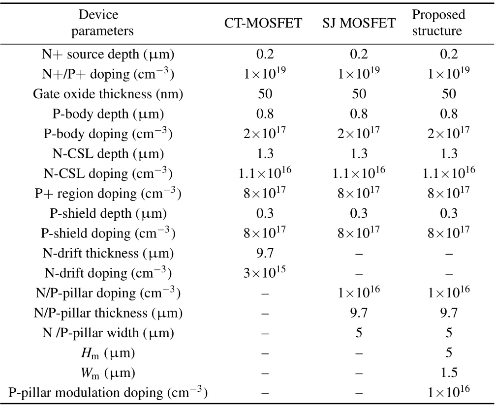
Table 1. Detailed structure parameters of devices.
To achieve more accurate simulation results, a series of physical models including Shockley-Read-Hall (SRH),Auger recombination, anisotropic avalanche (Okuto-Crowell model), incomplete ionization, and mobility degradation by the normal electric field (Enormal) are added in simulation settings. In addition, the thermodynamic model is employed to describe the electrothermal coupling behavior when the device is subjected to a high current density during the SC process. The active area of the chip in this paper is designed with 35 mm2.

Fig.2. The main fabrication flow of two structures: (a)the SJ structure and(b)the proposed structure with the partially widened pillar.
3. Results and discussion
3.1. Static parameters
Figure 3 illustrates the simulation results of static characteristics for the aforementioned three MOSFETs. From Fig.3(a), it can be seen that theVthcurves of the three structures almost completely overlap, and theVthof all devices atIds=1 mA is maintained at 2.19 V owing to the same structure and doping concentration of the channel region. Figure 3(b)shows that the breakdown voltages (BV) for three structures atIds=1 μA are 1913 V, 1836 V, and 1802 V, respectively.All of the structures meet the basic requirement of the 1.2 kV device design. A little lowerBVvalue in SJ structure can be noted,which is consistent with the previous study.[20]
According to the simulation results ofI-Vcharacteristics shown in Fig.3(c),the on-state resistance(Ron)at the current of 30 A are 40.2 mΩ,25.4 mΩ,and 29.3 mΩ,respectively. It is worth noting that theRonof the proposed structure is slightly higher compared with the conventional SJ MOSFET due to the narrowing of the current path induced by the partially widened pillar region. But thisRonvalue is obviously smaller than the CT-MOSFET due to the advantages of the N-pillar. In addition,the Baliga’s figures of merit(Baliga’s FOM=BV2/Ron)of all structures are calculated to evaluate overall static performance. It can be found in Table 3 that the Baliga’s FOM of SJ MOSFET and the proposed structure are increased by 46.2%and 22%compared with the CT-MOSFET,respectively.Therefore, the proposed structure can maintain a good static ability owing to the advantages of the SJ structure.

Fig.3. The comparison of simulation results(a)the threshold voltage,(b)the breakdown voltage,(c)the forward I-V characteristic and(d)the saturation characteristic.
As given in Fig.3(d),theIdsfor three structures atVds=800 V are 287 A, 278 A and 247 A, respectively. The saturation current value of the SJ MOSFET is close to that of the CT-MOSFET, indicating a similar SC ability. However, the saturation current of the proposed structure is significantly reduced. Under the highVds, the widened P-pillar depletes the N-pillar further and narrows the current path, resulting in the lower saturation current in the proposed structure.Therefore,a superior SC capability at the high drain voltage can be demonstrated.
In addition,it can be noted in Fig.3(d)that an incomplete saturation state of theIdscurves is found with the increase of drain voltage.The reason is related that the P+area blocks the depletion layer extension in the P-body during the increasing ofVds.Therefore,the pinch-off effect of the channel is affected inevitably,resulting in an incomplete saturation condition.
3.2. Optimization of pillar doping concentration in the SJ MOSFET
Obviously,the pillar doping concentration will influence the device characteristics in the SJ MOSFET. It is necessary to select an appropriate pillar doping concentration to achieve optimal performance, and the N-pillar and P-pillar have the same width to maintain charge balance. The static parameters with the variation of pillar doping concentration are illustrated in Fig.4.

Fig.4. The static performance of the SJ MOSFET with different pillar doping concentrations.

Table 2. The simulation results of the SJ MOSFET with varied pillar doping.
The exact values of the static parameters, the Baliga’s FOM, and the saturation current atVds=800 V are given in Table 2.
As shown in Fig. 4, theRonandBVof the SJ MOSFET decrease gradually with the pillar doping concentration increasing from 5×1015cm-3to 5×1016cm-3. TheBVdecreases quickly when the pillar concentration exceeds 4×1016cm-3, and theRonpresents a sudden increase when the pillar concentration drops to 5×1015cm-3. Meanwhile,the saturation current of the SJ structure is higher than that of the CT-MOSFET when pillar concentration exceeds 1×1016cm-3from Table 2, indicating a poor SC characteristic. Therefore,the value of 1×1016cm-3is the optimal pillar doping concentration of the SJ structure in this simulation MOSFET after the selection between Baliga’s FOM and SC ability.
3.3. The SC simulation results and analysis of the three different structures
The circuit of short-circuit mixed-mode simulation is shown in Fig.5. The parameters are set as follows: the parasitic inductance (Lp) is 200 nH, the DC drain-source voltage is 800 V[6,13,14], and the gate resistance (Rg) is 2.5 Ω. The single pulse gate voltage of 15 V/0 V with varied pulse times is applied to control the SC times. The simulation waveforms of the drain-source voltage (Vds), the drain current (Ids), and the lattice temperature (Tmax) are captured to inspect the SC performance.

Fig.5. Schematic of circuit used for SC simulation in this paper.
The SC waveforms under different gate pulses of the CTMOSFET are shown in Fig.6. It is found that theIdsgradually decreases to 0 A atTpulse=15 μs, which means the device is at normal turn-off condition. Once the gate pulse time(Tpulse)increases to 16 μs, theIdscannot drop to 0 A and shows a gradual increase at the final time of the SC process,indicating an abnormal turn-off process. Furthermore,it can be seen that a rapid increase of theIdswhen theTpulseincreases to 20 μs,resulting in a severe burnout failure. Therefore, the SC withstand time(SCWT)of the CT-MOSFET is 15μs,and the SC saturation current is about 495 A,as given in Fig.6.

Fig. 6. The SC simulation results of the CT-MOSFET under different gate pulses.

Fig. 7. The SC simulation results of the SJ MOSFET under different gate pulses.
A similar situation of the SJ MOSFET can be found in Fig.7. The SC saturation current of the SJ MOSFET is about 460 A,which is slightly lower than that of the CT-MOSFET.Thus, the SCWT of the SJ MOSFET is 17μs. The SJ MOSFET shows a slightly better SC performance than the CTMOSFET,which is consistent with the results given by Okadaet al.[17]
Figure 8 shows that the SC saturation current of the proposed structure is about 360 A, which is much less than the other two structures. The SCWT is increased to 24 μs,which is improved by 60%and 41.2%compared with the CTMOSFET and SJ MOSFET,respectively.All parameters comparison of the three structures obtained from the simulation is summarized in Table 3.
It can be inferred from the above discussion that the burnout failure occurs after the devices are subjected to a harsh SC pressure. The internal lattice temperature rises rapidly due to the high SC current and voltage, then the electro-thermal coupling effect with the positive feedback phenomenon will occur continually. After a long SC time,the current inside the device still rises sharply even if the gate is turned off,resulting in the dynamic avalanche breakdown and heat accumulation at the local region. Thus, this failure is directly affected by the magnitude of the SC current, and the device with a lower SC current demonstrates a robust SC withstand ability.

Fig. 8. The SC simulation results of the proposed structure under different gate pulses.

Table 3. The simulation results of the three different MOSFETs.
3.4. Analysis of the physical mechanism inside the devices
To analyze the inner physical mechanism of different SC abilities,as shown in Fig.9,the same gate voltage pulse time of 20 μs is applied to the three structures. The distribution of the electric field, the total current density, and the lattice temperature at the time points 20 μs and 40 μs are obtained in Figs. 10, 11, and 12, respectively. From the comparison waveforms, the proposed structure can turn off safely, while the CT-MOSFET and the SJ MOSFET fail at this SC pressure.
From Fig. 9, it can be seen that theIdsincreases firstly and then decreases during the SC process. We believe that these changes are attributed to the channel mobility. The rise ofIdsat the beginning is related to the weakening of Coulomb scattering mechanism from two aspects. The inversion charge increases with the rise of lattice temperature when the channel is formed,and the influence of Coulomb scattering on carrier mobility was shielded by abundant free electrons. In addition,the trapped charge reduces due to the energy band narrowing with the lattice temperature rising, then the Coulomb scattering effect caused by the interface charged center is weakened. Subsequently,the continuous increase in lattice temperature leads to the increase of surface roughness scattering and phonon scattering, which in return causes the decrease of inversion layer carrier mobility and the subsequent decline of SC current.
As shown in Fig. 10, the distribution of electric field is changed due to the addition of the partially widened p-pillar.Most importantly, the cumulation of the electric field at the trench bottom area is suppressed. It can be seen that the high electric field is transferred to the bottom of the widened Ppillar region,which also helps to protect the gate oxide below the trench.

Fig.9.Comparative simulation results of the three different structures under the same gate pulse of 20μs,including the waveforms of Ids and Tmax.
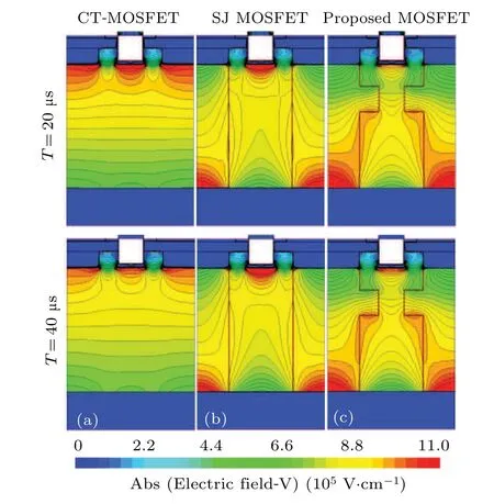
Fig. 10. Simulation results of electric field distribution inside the devices at time points 20μs and 40μs for(a)the CT-MOSFET,(b)the SJ MOSFET,(c)the proposed structure.
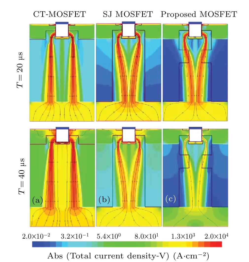
Fig. 11. Simulation results of total current density distribution inside the devices at time points 20μs and 40μs for(a)the CT-MOSFET,(b)the SJ MOSFET,(c)the proposed structure.
As depicted in Fig.11,the current flowing path of the proposed device is modulated compared with the CT-MOSFET and the SJ MOSFET. It can be seen that the widened Ppillar region squeezes the electron flowing path in the N-pillar,which is similar to the JFET effect in the planar DMOSFET.Meanwhile, when the proposed structure is under a highVds,the hot spot is transferred to the widened P-pillar region, as illustrated in Fig. 12. Therefore, the huge SC saturation current caused by the larger avalanche injection is weakened. Although, it can be seen that the current still flow within the widened P-pillar region due to the dynamic avalanche accumulation at that area. But the saturation current is suppressed effectively.
Fig.12. Simulation results of lattice temperature distribution inside the device at time points 20μs and 40μs for(a)the CT-MOSFET,(b)the SJ MOSFET,(c)the proposed structure.
Under the influence of electric field and current density,the internal peak junction temperature of the proposed structure is significantly lower than that of the CT-MOSFET and the SJ MOSFET at times 20 μs and 40 μs, as shown in Fig. 12.Consequently, the electro-thermal coupling effect with the positive feedback phenomenon is suppressed in the proposed structure,resulting in the improvement of the SC reliability.
3.5. Proposed structure parameters optimization
The influence of structure parameters in the proposed structure is investigated,including the position(Hm)and width(Wm)of the P-pillar modulation region.The doping concentration of the P-type region is fixed at 1×1016cm-3as the same with the aforementioned SJ MOSFET to avoid the complex fabrication variation and the over intensified JFET effect. According to the structure and cell pitch of the proposed MOSFET, theHmis adjusted from 4 μm to 7 μm and theWmis increased from 1 μm to 2 μm to analyze the device’s performance. Figure 13 shows the proposed MOSFET’s static parameters and saturation current varying withHmandWm,and the detailed simulation results are summarized in Table 4.
From Fig.13,it can be seen that theBVdegrades slightly with the descending of location (Hm) and the widening of width(Wm)for the P-pillar modulation region,which is caused by partial charge imbalance behavior. That means the changing of theBVis little with the variation ofHmandWmfor the small modulation region. Meanwhile, it is worth noting that theRonkeeps unchanged if theHmis over 5μm. On the contrary,theRonincreases sharply and the Baliga’s FOM degenerates severely once theHmdecreases to 4μm. The reason is that the current flowing path will be seriously suppressed when the position of the P-pillar modulation region is too close to the P-shield region. Moreover, theRongradually increases with the widening ofWm. The more obvious increase ofRonand the critical degradation of Baliga’s FOM are found at theWmof 2μm.
Figure 13(b) and Table 4 exhibit that the saturation current of the proposed structure gradually decreases with the rising of location (Hm) and the widening of width (Wm) for the P-pillar modulation region. That means the distinct suppression effect can be found if the P-pillar modulation region is close to the top side, bringing a better SC reliability. However, it may cause the sacrificing of the static performance as we mentioned before. After comprehensive consideration,theHm=5μm and theWm=1.5μm are selected as the optimal structural parameters by comparing static characteristics and SC performance.

Fig. 13. The (a) Ron and BV; (b) Baliga’s FOM and saturation current(Vds=800 V)of the proposed structure with different Hm and Wm values.

Table 4. The simulation results of the proposed structure with varied Wm and Hm.
4. Conclusion
In this study, a 1200 V SiC super-junction (SJ) MOSFET with a partially widened pillar is proposed to improve the SC capability. By investigating the static characteristics and the SC performance, it is found that the Baliga’s FOM(BV2/Ron) of the proposed structure increased by 22% compared to the conventional trench structure. Meanwhile, a superior SC performance is also achieved. Compared with the conventional trench structure and SJ structure, the SC withstand time (SCWT) of the proposed structure increased by 60%and 41.2%,respectively. The enhancement of SC ability is attributed to the suppression of the saturation current at the SC transient process without sacrificing the on-state current ability. In addition, the fabrication technology is compatible with the standard epitaxy growth method with simple implant window adjustment.
Acknowledgement
Project supported by the Key Research and Development Program of Guangdong Province, China (Grant No.2019B090917010).
猜你喜歡
中學(xué)生數(shù)理化·自主招生(2023年5期)2023-04-26 15:48:00
知音(月末版)(2021年5期)2021-05-28 13:41:38
Journal of Donghua University(English Edition)(2020年2期)2020-06-04 06:24:12
知音(月末版)(2019年7期)2019-07-27 01:31:09
課堂內(nèi)外·創(chuàng)新作文高中版(2018年1期)2018-01-29 18:51:15
天津詩人(2017年2期)2017-11-29 01:24:14
試題與研究·高考理綜物理(2016年3期)2017-03-28 21:08:11
小溪流(畫刊)(2015年11期)2015-12-12 00:14:09
新作文(小學(xué)中高年級版)(2015年5期)2015-04-12 06:27:45
雕塑(1997年2期)1997-06-30 08:58:28

- Chinese Physics B的其它文章
- Erratum to“Accurate determination of film thickness by low-angle x-ray reflection”
- Anionic redox reaction mechanism in Na-ion batteries
- X-ray phase-sensitive microscope imaging with a grating interferometer: Theory and simulation
- Regulation of the intermittent release of giant unilamellar vesicles under osmotic pressure
- Bioinspired tactile perception platform with information encryption function
- Quantum oscillations in a hexagonal boron nitride-supported single crystalline InSb nanosheet